RESEARCH OUTPUTS / RÉSULTATS DE RECHERCHE
Author(s) - Auteur(s) :
Publication date - Date de publication :
Permanent link - Permalien :
Rights / License - Licence de droit d’auteur :
Bibliothèque Universitaire Moretus Plantin
Institutional Repository - Research Portal
Dépôt Institutionnel - Portail de la Recherche
researchportal.unamur.be
University of Namur
Nanophotonics for ultra-thin crystalline silicon photovoltaics: when photons (actually)
meet electrons
Depauw, Valérie; Abdo, Islam; Boukhicha, R; Cariou, Romain; Chen, W.; Bolanos, I. Cosme;
Deparis, Olivier; Ding, He; Dmitriev, Alexandre; Drouard, Emmanuel; El Daif, Ounsi; Fave, A.;
Foldyna, Martin; Garcia-Caurel, Enric; Heidary, B.; Herman, Aline; Lalouat, Loic; Lee, Ki
Dong; Liu, J.; Lodewijks, Kristof; Mandorlo, Fabien; Massiot, Inès; Mayer, Alexander; Muller,
Jérôme; Narchi, P.; Orobtchouk, Regis; Picardi, G.; Prod'Homme, Patricia; Roca i
Cabarrocas, Pere; Seassal, Christian; Trompoukis, Christos; Gordon, I.; Poortmans, Jef
DOI:
10.4229/EUPVSEC20142014-3BO.6.5
Publication date:
2014
Document Version
Early version, also known as pre-print
Link to publication
Citation for pulished version (HARVARD):
Depauw, V, Abdo, I, Boukhicha, R, Cariou, R, Chen, W, Bolanos, IC, Deparis, O, Ding, H, Dmitriev, A, Drouard,
E, El Daif, O, Fave, A, Foldyna, M, Garcia-Caurel, E, Heidary, B, Herman, A, Lalouat, L, Lee, KD, Liu, J,
Lodewijks, K, Mandorlo, F, Massiot, I, Mayer, A, Muller, J, Narchi, P, Orobtchouk, R, Picardi, G, Prod'Homme, P,
Roca i Cabarrocas, P, Seassal, C, Trompoukis, C, Gordon, I & Poortmans, J 2014, 'Nanophotonics for ultra-thin
crystalline silicon photovoltaics: when photons (actually) meet electrons', Paper presented at 29th European
Photovoltaic Solar Energy Conference and Exhibition, Amsterdam, Netherlands, 22/09/14 - 26/09/14 pp. 1461.
https://doi.org/10.4229/EUPVSEC20142014-3BO.6.5
General rights
Copyright and moral rights for the publications made accessible in the public portal are retained by the authors and/or other copyright owners and it is a condition of accessing publications that users recognise and abide by the legal requirements associated with these rights. • Users may download and print one copy of any publication from the public portal for the purpose of private study or research. • You may not further distribute the material or use it for any profit-making activity or commercial gain
• You may freely distribute the URL identifying the publication in the public portal ?
Take down policy
If you believe that this document breaches copyright please contact us providing details, and we will remove access to the work immediately and investigate your claim.
NANOPHOTONICS FOR ULTRA‐THIN CRYSTALLINE SILICON PHOTOVOLTAICS: WHEN PHOTONS (ACTUALLY) MEET ELECTRONS
V. Depauw*1, I. Abdo1, R. Boukhicha2, R. Cariou2, W. Chen2, I. Cosme Bolanos2, O. Deparis3, He Ding5, A. Dmitriev4,
E. Drouard5, O. El Daif1,┴, A. Fave6, M. Foldyna2, E. Garcia‐Caurel2, B. Heidari7, A. Herman3, L. Lalouat5, K. D. Lee7, J.
Liu5, K. Lodewijks4, F. Mandorlo6, I. Massiot4, A. Mayer3, J. Muller3, P. Narchi2, R. Orobtchouk6, G. Picardi2,
P. Prod’Homme8, P. Roca i Cabarrocas2, C. Seassal5, C. Trompoukis1, 9, I. Gordon1, J. Poortmans1, 8, 10 1 Silicon Photovoltaics, Imec, Kapeldreef 75, B-3001 Leuven, Belgium
2 LPICM‐CNRS, Ecole Polytechnique, 91128 Palaiseau, France
3 Laboratoire de Physique du Solide, University of Namur, Rue de Bruxelles 61, 5000 Namur, Belgium 4 Applied Physics, Chalmers University of Technology, Gothenburg, Sweden
5 Université de Lyon; Institut des Nanotechnologies de Lyon INL UMR5270, CNRS; Ecole Centrale de Lyon; Ecully,
F-69134, France.
6 Université de Lyon; Institut des Nanotechnologies de Lyon INL UMR5270, CNRS; INSA Lyon; Villeurbanne,
F-69621, France.
7 Obducat Technologies AB, Lund, Sweden 8 Total M&S. – New Energies, R&D division, Paris, France 9 Departement Elektrotechniek – ESAT, KULeuven, Leuven, Belgium
10 UHasselt, Hasselt, Belgium
┴ Now with Qatar Environment and Energy Research Institute, Doha, Qatar
*Corresponding author: tel +32 16 28 82 65, fax +32 16 28 15 01, valerie.depauw@imec.be
ABSTRACT: Nanopatterning has recently demonstrated to be an efficient method for boosting the light absorption of thin films (< 50 µm) of crystalline silicon. However, convincing solar cell results are still missing. The goal of the European project PhotoNVoltaics is to investigate the impacts that nanopatterns have on thin crystalline silicon solar cells and to identify the conditions for their efficient integration. The present contribution presents the main findings of the consortium so far.
Optical modeling and optimization of nanopatterned thin-film c-Si cells have indicated a few trends regarding the design of the optimum pattern for 1-40 µm thin foils: merged inverted nanopyramids, with their progressive profile seem to provide the best combination of antireflective and light trapping properties, together with negligible surface damage and best coating template for subsequent process steps. But despite the high Jsc enhancement that these nanopatterns are expected to bring, and despite the higher efficiency of these nanophotonic structures for 1-2 µm-thin foils, the absolute Jsc values indicate that thicker foils will have to be preferred if direct competition with wafer-based and thin-film technologies is concerned. An ideal structure is taking shape as an IBC heterojunction cell, with a front-side nanopattern and a thickness of 40 µm.
Keywords: Light trapping, Thin Film Solar Cell, Texturisation, Simulation, Nanopatterning
1 INTRODUCTION
Lately, many studies have discussed how the “Lambertian limit” of light trapping may be overcome by texturing crystalline silicon (c-Si) solar cell surfaces at the light wavelength scale, rather than at the micron-scale. Various simulations of periodic or non-periodic nanopatterns indicate, in fact, that significantly higher photon absorption may be achieved compared to micron-scale texturing, especially for absorber thicknesses below 100 µm. However, fewer publications present solar cells, and even fewer present solar cells with clearly higher energy-conversion efficiencies, thus showing that higher photon absorption does not readily translate into a higher electron collection. Nanopatterns are in fact challenging to integrate, because of the electrical degradation they introduce, and because of the optical degradation that they may undergo in later process steps. This integration challenge is yet inevitably to be overcome if thin c-Si foils are set to eventually replace wafers. This requires (i) modelling in order to identify the nanopatterns that provide the best photon absorption, (ii) fabricating these nanopatterns under the various experimental constraints set by the materials, and (iii) integrating such nanopatterns into solar cells without compromising their electrical performances (with the highest short-circuit
currents and open-circuit voltage possible). Finally, suppressing the hurdle of light-absorption losses in thin film c-Si solar cells requires (iv) assessing the boundary conditions for an industrially-compatible nanopatterning and solar-cell process. That, is the objective of the European project PhotoNVoltaics.
We give here an overview on learning points that we have identified so far for reaching the best light-harvesting nanopatterned c‐Si solar cells of 1 to 40 µm thickness. These learning points relate to the three first work domains listed above, namely modelling (Section 3), nanopatterning (Section 4) and cell integration (Section 5). Their outcomes are combined into the perspectives (Section 6), a solar cell extracting 40 mA/cm2 from 40 µm of c-Si. The framework is
introduced in the next section.
2 PROJECT APPROACH AND THIN-FILM C-SI The approach of PhotoNVoltaics for identifying the thin-film c-Si cells that have the potential to compete with wafer-based photovoltaics (PV), is to sweep a maximum of possibilities, both in terms of nanopattern types and in terms of c-Si thin film types. The thin-film types cover monocrystalline and polycrystalline foils, grown by high and low-temperature CVD, with and
without layer-transfer techniques, and go from 1 µm up to 40 µm thickness [1]–[4]. All these layers are held by a carrier substrate, thus eliminating the handling issues of processing thinner wafers, while enabling the processing at module level. The nanopatterns, periodic and non-periodic, are the result of various combinations of three lithography and three etching techniques. The solar cell technology for their integration is an a-Si:H/c-Si heterojunction emitter cell (HET).
One should note that these c-Si cells are based on a purely crystalline material as wafer-based cells, monocrystalline or polycrystalline with grains larger than 100 µm. It does not present any amorphous phase, like thin-film microcrystalline-silicon cells, which have different optical and electrical properties (e.g. refractive indices and minority-carrier recombination lifetime). It is thus an intermediate between the c-Si bulk technology and the amorphous and microcrystalline technology, sharing respectively their material quality and thickness range.
3 IDENTIFYING THE BEST NANOPATTERNS BY MODELLING
Computer modelling is the most convenient approach, in terms of time and effort, for identifying the most beneficial nanopattern morphology (i.e. its pitch, filling fraction, and profile shape) to reach the highest short-circuit current (Jsc) possible for a specific solar cell architecture. We present a few trends of nanopattern designs that could be extracted from a first optimization campaign, after illustrating two aspects that may seem obvious, but that should not be forgotten when analyzing simulation results.
3.1. Optimizing the right figure of merit
3.1.1. Calculating the absorptance of active layers only Optical simulations typically outcome the photon absorptance of the given structure. Absorptance is also the value that can be measured most straightforwardly in experiments. However, the absorptance of the complete stack (with ARC, rear-reflector, ...) is not directly giving an output of the Jsc, since only a few of the layers will actually generate electrons that can be collected by the contacts. Extraction of the actual figure of merit, the Jsc, requires isolating the number of photons that are absorbed in electrically active layers, i.e. in our case the c-Si base.
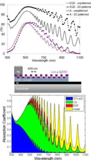
For example, as can be seen in Figure 1, the 1-µm-thin c-Si solar cell below showed a very high absorptance on long wavelengths after nanopatterning its front side. But its external quantum efficiency (EQE) demonstrates that it did not translate into collected electrons. As displayed in the breakdown calculation of the stack absorption, a large part of the photons was in fact absorbed in a non-active zone, the Al rear contact. One may see that the transparent conductive oxide (TCO) and the a-Si:H emitter also absorbed a significant part of the light on the short wavelength [5].
Figure 1: (top) Absorptance and EQE of a 1-µm-thin
solar cell (middle) with a flat or nanopatterned front surface. (bottom) Modeled localized absorption spectra of the unpatterned cell in terms of absorption efficiency, isolating the contributions of each layer.
3.1.2 Matching the model to the actual (imperfect) experimental cell
When defining the modeled stack, many simplification assumptions are made, such as taking a perfectly geometrical shape for the holes, considering flat interfaces, uniform layer thickness or pattern diameter, ... which are valid only to a certain extent in representing the experimentally fabricated samples. It is important to check whether these assumptions have a strong influence on the end result.
The calculated Jsc in [5], for instance, was calculated to go from 15.60 with a perfectly conformal ITO layer down to 13.34 mA/cm2 with a non-continuous coating.
The actual conformality of the layers was hence verified experimentally to design the best-matching model. 3.2 Optimization maps
Optimization maps of thin-film cells with three different thicknesses and two etch profiles (Fig. 2), were modeled by RCWA or FDTD for the super-gaussian holes and the inverted nanopyramids, respectively. This study was based on the calculation of the light-absorption efficiency of the cell:
where a and i are respectively the absorbed photon
flux and the incident photon flux, A(λ) is the absorption coefficient in the active layer (given by simulations by FDTD or RCWA) and S(λ) is the normalized solar spectrum AM1.5G. Under the hypothesis of a perfect internal quantum efficiency, the short circuit current density of the cell is Jsc = ea where e is the charge of
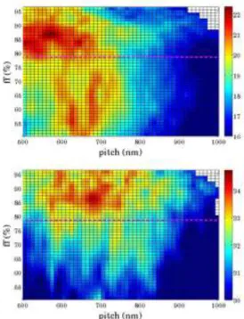
the electron. It can be noticed that a complete sunlight absorption by the silicon would lead to a Jsc of 43.5 mA/cm². In order to maximize this Jsc, the optimization was performed by parameter scans. This scanning map allows determining large areas of optimum values, in order to take into account the experimental profile tolerances. The outcome for each film thickness is shown in Figure 3 for super-gaussian holes and a comparison between the two profiles can be found in Table I.
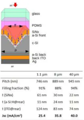
Figure 2: Optimized solar cell structure with
super-gaussian holes (left) and inverted nanopyramids (right), composed from top to bottom of ITO (orange), a-Si:H (light grey), the patterned c-Si active layer (grey), c-Si back-surface field (dark grey), ITO rear-buffer layer (orange) and Al.
Figure 3: Jsc maps in mA/cm2 by scanning the filling
fraction ff and the pitch with a front-side 2D nanopattern with super-gaussian holes. The thickness of the active c-Si layer was set to 1.1 µm, 8 µm and 40 µm (from top to bottom). The dashed line gives the limit above which the holes start to merge.
Table I: Highest calculated Jsc for two c-Si thicknesses
and nanopatterned with inverted nanopyramids or super-gaussian holes.
c-Si film / Jsc (mA/cm2) 1.1 µm 8 µm 40 µm
Super-Gaussian holes 22.1 34.4 39.0 Inverted nanopyramids 23.6 35.0 39.2
We can observe the following trends:
- Higher Jsc are obtained with higher filling fraction (i.e. above purple line). Not surprisingly, this trend fits the need for a small amount of flat surface, for a more progressive index variation in depth.
- Probably for the same reason, nanopyramids, with the most progressive profile, deliver a higher absorption than super-gaussian holes [6].
- The optima windows differ for each thickness, but a common “sweet spot” can be found around 700 nm pitch. The 1 µm case differs more and presents a second optimum window at a lower filling fraction that the others. This can be explained by the fact that, at this thickness, front and rear sides of the sample can interact better, with richer photonic effects [7]. These trends let us conclude that the best nanopattern seems to be inverted nanopyramids that are perfectly merged. Not surprisingly, the interesting photonic effects are mostly efficient for micron-scale films. Unfortunately, micron-thin films still deliver a significantly lower Jsc than thicker foils, despite the strong improvement from the nanopattern.
4 FABRICATING IDEAL NANOPATTERNED SURFACES
The nanopatterns are formed by combining a lithography technique, to define the pattern, with an etching technique, to transfer the pattern into the silicon surface. Our lithography techniques are i) laser-interference lithography (LIL) [8] for quickly adaptable small-scale patterns, ii) nanoimprint lithography (NIL) [9] for wafer-scale imprint with potential up-scaling to industry, and iii) hole-colloidal lithography (HCL) [10], for controlled pseudo-periodic patterns with short-range order. The etching techniques are either dry plasma
etching (ICP and RIE) or wet chemical etching (TMAH). These combinations, and particularly the possibility of controlling the etch profiles by tuning the etching conditions, lead to a large variety of nanopatterns for a wide range of textures. Currently, cost-calculations for these methods are on-going to determine if they could potentially be transferred to the PV industry, and under which conditions.
We present below two experimental boundary conditions that limit the pattern quality and the various reflectance curves that these combinations have delivered so far.
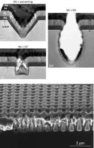
4.1 Taking into account imperfections of etch processes Most nanopatterning methods require a lithography step to define the pattern position, and they are thus often dependent on the surface roughness. This can be an issue in certain types of c-Si films, such as polycrystalline Si, as illustrated in Figure 4, where standard NIL results in a lower surface coverage, around 75%, which visibly alters the light trapping effect. HCL, on the other hand, is perfectly suited and leads to a coverage near to 100%. The NIL process may also be adapted for more conformality (e.g. reversal imprint, or substrate conformal imprint lithography).
Figure 4: HCL-patterned (left) and NIL-patterned (right)
polycrystalline-Si sample with a roughness of 250-500 nm (rms) leading to a pattern coverage of almost 100% and 75% respectively.
Another limitation that should be noted is related to the wet-etching processes. Wet etching, which is crystal-orientation dependent, results in formation of pyramidal profiles following the {111} planes. It is an important process since it can provide the best optical properties, (and as discussed later also better electrical properties) provided a high filling fraction (ff) can be reached. If perfectly aligned holes may reach 95% of ff with an imprint perfectly aligned to the crystal planes, pseudo-periodic holes may not allow it. In fact, the irregular distance between pyramids leads locally to their merging into larger pyramids (Figure 5), which alter the optical properties and may limit the (theoretically) promising performance of these pseudo-periodic nanopyramids.
The limitations can be taken into account when opting for a nanopattern from optical calculations, and that leads to checking the sensitivity to the parameters and selecting wider windows of Jsc (though lower), rather than aiming at a few tens of extra mA/cm2 in a
more challenging zone.
Figure 5: Undesired merging of inverted nanopyramids
in a pseudo-periodic pattern, leading to inverted micron-scale pyramids, with lower light trapping properties. 4.2 Experimental reflectance curves
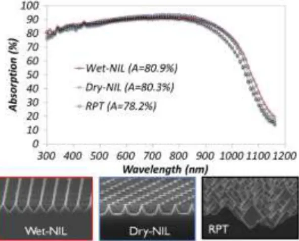
An example of wet-NILed nanopatterned film, compared to the benchmarking standard texture of micron-scale random pyramids is shown in Figure 6. The sample is a bare foil with a textured front side that was bonded to glass with a highly transparent silicone. The absorptance measurement – in which we can assume the absence of parasitic absorption - shows clearly that the nanopattern leads to a better collection of longer wavelength photons than the random micron-scale pyramids. However the antireflective properties, visible from the shorter wavelength, are not improved or even less good.
Figure 6: Absorptance curve of a bare 40-µm-thin c-Si
foil textured with random micron-scale pyramids and nanoimprinted structures with parabolic-shaped holes (dry-NIL) and inverted nanopyramids (wet-NIL).
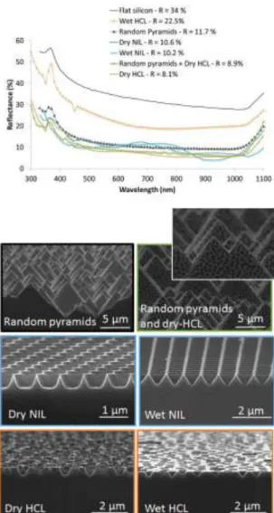
These antireflective properties can be compared by patterning a thick wafer (700 µm) with various patterns, without ARC. These results are benchmarked on Figure 7. Combinations of wet and dry etching with ordered (NIL) or pseudo-ordered (HCL) structures are shown. An alternative texture, dry-HCL on random pyramids, is also shown, that combines wave optics and ray optics, and demonstrates the perfect conformality of HCL, even on such a large-scale corrugation. We may see that the reflectance can be decreased as compared to random pyramids, but only with a careful control of the filling fraction (cf. wet-HCL and dry-HCL curves). Eventually, one may note that random-pyramid texturing (RPT) is a challenging benchmark, if it can actually be applied to the foil (i.e. where one may afford to lose 5 µm of material during the etching step). If not, in the case of
ultra-thin films or expensive deposition techniques, nanopatterning efficiently fulfills its light trapping duty consuming only a few hundreds of nm.
Figure 7: Reflectance and SEM of various
non-optimized combinations of lithography and etching on wafers, without ARC, including a comparison with conventional random pyramid texturing.
5 INTEGRATING THE NANOPATTERNS INTO SOLAR CELLS
The nanopattern has an impact both on the electrical performance of the material itself and on those of the coatings on top. So far, the typical trend in cell performances when integrating nanopatterns is a higher Jsc, and a drop in open-circuit voltage (Voc). As in the example below, the fill factor (FF) can sometimes also be significantly affected. Overall, the energy-conversion efficiency (η) stays constant or may even drop [11].
Figure 8: Solar cell stack of 4 µm grown by
low-temperature PECVD on a highly-doped (non-active) p++
Si wafer [2].
Table II: Measured I-V performances of PECVD-Si
solar cells with wet- and dry-etched front nanopatterns. Texturing Jsc [mA/cm2] Voc [mV] FF [%] η [%] Flat 15.9 492 74.9 5.9 Dry-NIL 6.9 393 57.5 1.5 Wet-NIL 19.9 501 79.2 7.8 5.1 Controlling surface recombination velocities
The challenge of surface passivation is today a well-known issue for nanopatterning. In fact, a degradation of surface recombination velocity is often observed, due to the increase of surface area, the difficulty of passivating the corrugations, and the damage induced by dry-etching methods. Solutions that are being proposed in the field are rather broad: avoiding the texturing of silicon and applying the nanopattern on dielectrics deposited on top of a passivated flat silicon surface [12], limiting the etched area [13], using conformal passivation and/or tuning the etching conditions so as to limit [14] or avoid the damage [15], or then treating the surface damage [16].
In the case of our wet-etched inverted nanopyramids, we have demonstrated that a surface recombination velocity as low as 8 cm/s can be reached with a-Si:H as passivating layer [6]. As for dry-etching however, we have not yet been able to passivate it as efficiently, especially for deeper corrugations, which are more efficient from an antireflection point of view. One of the possible reasons is the insufficient a-Si:H conformality, as discussed below.
5.2 Taking into account conformality of coatings The materials deposited on top of the nanopatterned c-Si film can be affected by its topography, depending on the deposition technique (ALD, PECVD, sputtering, thermal evaporation etc...), which can affect their properties. This is why ALD has often been proposed as a solution for passivating demanding surfaces. However, not only passivation but also other coatings are affected.
Figure 9: (top) TEM of nanopatterned Si wafers with
different etched profiles, showing that the thickness uniformity is affected for all materials, possibly leading to a discontinuity of the coating. (bottom) SEM view, showing the voids inside the metal layer.
A TEM investigation was performed in order to check the thickness uniformity of various coatings along the pattern. In the present case, a-Si:H, ITO, and Ti/Pd/Ag were deposited by PE-CVD, sputtering and e-beam evaporation, respectively. As expected, deeper and more vertical patterns prevent the continuity of the layers. The inverted nanopyramids present the most favorable case, where all layers are continuous (though the presence of local holes in the Pd layer could be noted). In the deepest structure, etched by RIE, the metals do not even contact the bottom of the hole and only 2-3 nm of ITO are present on the sidewalls. Continuity of a-Si:H is ensured in all cases, however its thickness also drops to a few nm only, which most probably affects the passivation.
Macroscopically, the conformality of the contacting layers translates into an increase of the cell’s series resistance (participating to the drop in FF, as seen in Table II). TLM measurements confirm that the sheet resistance of the ITO-Ti/Pd/Ag stack increases significantly on a dry-etched profile, from 50 to 80 Ω/sq [17]. This increase can be attributed to the non-conformality of the ITO rather than to the non-continuity of the metal alone, whose sheet resistance is not significantly affected by the voids. On a microscopic level, however, the non-uniformity of the coatings may have a stronger impact on the local fields, which will have to be investigated further.
6 FURTHER CELL OPTIMISATION
When taking all of these learnings into account, the conclusion for the design of a high-performance thin-film c-Si leads us to a heterojunction interdigitated back-contact cell (IBC), with a front-side nanopattern of inverted pyramids. In fact, as observed above, the nanopyramids formed by wet etching enable reaching very low recombination velocities, have excellent optical properties and degrade the less the coating properties. Then, positioning the emitter at the rear side would avoid the need for a TCO at the front side (which can absorb an important fraction of photons in the 300-600 nm range as shown in Fig. 1) and of patterning the (sensitive) emitter [18]. Secondly, putting all contacts on the rear-side makes processing more straightforward because of the presence of a foreign substrate, it eases module processing and prevents shadowing losses. Finally, the choice of a heterojunction derives from the need for low-temperature processes with a (low-cost) foreign substrate, so as from the strong need for excellent passivation in thin devices.
A few questions on the design of this IBC cell are discussed below.
6.1 Optimization by a genetic algorithm
An optimization campaign was run to define the optimum nanopattern and layer thicknesses that this structure would require, for three film thicknesses of 1.1 µm, 8 µm and 40 µm. This time, rather than simple scans, in order to explore a complete set of parameters in combination, a genetic algorithm developed at the University of Namur was used [19]. This method enables the collective exploration of a broad range of parameters, without enduring an exponential explosion of computing time. The strategy consists in selecting from generation to generation the fittest individuals of a population (each individual is representative of a given set of parameters). New individuals are generated by crossing these selected individuals and by introducing random mutations in the coding of parameters. By this evolutionary strategy, the population generally converges to globally optimal solutions. The preliminary results of the calculation (Figure 10) confirm that an optimum nanopattern with random pyramids requires a high filling fraction (>85%). A Jsc of 40 mA/cm2 (or slightly higher as the calculations
Figure 10: IBC cell stack modeled by RCWA and Jsc
resulting from the genetic algorithm optimizing the absorptance of the c-Si films of 3 different thicknesses, and the corresponding variable values. These values are not yet the fully optimized ones, the algorithm being in the final refining step at this moment.
Nevertheless, this Jsc is still higher than the actual that may be expected from a real device. In fact, if the model takes into account the experimental limitations for the nanopattern fabrication (ff of 95% achievable at most via TMAH etching, non-uniform ITO thickness along the walls,...), real experimental optical constants, and practical boundaries for the cell stack thicknesses, it does also consider a (non-real) perfect electron collection efficiency of 100% over the whole spectrum. A future step will therefore be to take into account carrier losses in the device.
6.2 Further minimizing the front-side losses
The photon absorption breakdown in the whole device above (Figure 10) shows that the highest parasitic absorptance, despite the replacement of a TCO by SiNx as ARC, is still originating from the front-side, and more specifically from the a-Si:H. A way of gaining a few tenths of mA may therefore be to replace it by a less absorbing passivating layer. AlOx may be an option but the requirement for a post-anneal and its lower efficiency on n-type devices makes it a non-ideal candidate. Another option would be to alloy this a-Si:H, as proposed in [20]. Preliminary results on wafers show an encouraging maintenance of FF and Voc, while increasing the Jsc, which leads to an outstanding 17.7% efficiency for a flat solar cell (Fig. 11)
Figure 11: Stacks and J-V curves of heterojunction
emitter wafer-based cells with standard a-Si:H emitter and lower-absorptance a-SiOx:H emitter.
6.3 Single-side texturing or double-side texturing? We have so far only discussed the patterning of the front-side of the thin film c-Si cells. However, double-side patterning may also be performed and may be expected to bring a significant boost, although that is in practice more difficult than for wafer-based cells, since the carrier substrate limits the access to a single side at a time, and more than for a-Si/µc-Si cells, since the crystalline film cannot be grown on corrugated substrates. In the present case, the bonds between the film and its parent wafer or its carrier thus set strong “boundary conditions” on the nanopatterning, to avoid damage to the fragile foil. A set of FDTD simulations performed on a dual-patterned structure showed that the relative improvement in Jsc gained from a rear pattern, with respect to an optimized front-side pattern, quickly drops with film thickness as shown in Figure 12. For a film of 8 µm, the improvement would be less than 5% relative. Consequently, the foils that would provide the highest Jsc, with thicknesses above 6 µm, are those which would benefit the less from a dual pattern. It may thus be difficult for that little boost in Jsc to compensate for the extra costs related to the extra processes involved.
Figure 12: (left) 1D Double-side patterned thin film solar
cell. (right) Simulated Jsc as a function of the thickness of the Si active layer for double-side patterned cells, and relative enhancement compared to the front patterned cell having the same Si thickness.
Finally, an extra boost in Jsc as compared to the values given above may be expected from the use of “optimally disordered” nanopatterns. It seems in fact
from recent studies that, between perfect order and randomness, the optimum light trapping would lie in between, with pseudo-periodic (such as those prepared by HCL) or quasi-random structures [21]. Further work is however needed to demonstrate whether the enhancement may still be significant for films thicker than 1 or 2 micrometers, and whether simple fabrication methods may be found.
7 CONCLUSION
Optical modeling and optimization of nanopatterned thin-film c-Si cells have indicated a few trends regarding the design of the optimum pattern for 1-40 µm thin foils: merged inverted nanopyramids, with their progressive profile seem to provide the best combination of antireflective and light trapping properties, together with negligible surface damage and best coating template for subsequent process steps. But despite the high Jsc enhancement that these nanopatterns are expected to bring, and despite the higher efficiency of these nanophotonic structures for 1-2 µm-thin foils, the absolute Jsc values indicate that thicker foils will have to be preferred if direct competition with wafer-based and thin-film technologies is concerned. An ideal structure is taking shape as an IBC heterojunction cell, with a front-side nanopattern and a thickness of 40 µm.
8 ACKNOWLEDGMENTS
This project has received funding from the European Union’s Seventh Framework Programme for research, technological development and demonstration under grant agreement No 309127, PhotoNVoltaics (www.photonvoltaics.org).
Part of this research used resources of the "Plateforme Technologique de Calcul Intensif (PTCI)" (http://www.ptci.unamur.be) located at the University of Namur, Belgium, which is supported by the F.R.S.-FNRS under the convention No. 2.4520.11. The PTCI is member of the "Consortium des Équipements de Calcul Intensif (CÉCI)" (http://www.ceci-hpc.be)."
The Imec team acknowledges Jef Geypen and Hugo Bender for the TEM investigation.
9 REFERENCES
[1] K. Van Nieuwenhuysen, V. Depauw, R. Martini, J. Govaerts, M. Debucquoy, H. Sivaramakrishnan Radhakrishnan, I. Gordon, T. Bearda, K. Baert, and J. Poortmans, “High Quality Epitaxial Foils, Obtained by a Porous Silicon Based Layer Transfer Process, for Integration in Back Contacted Solar Cells,” Proc. 27th Eur. Photovolt.
Sol. Energy Conf. Exhib., pp. 2471 – 2474, Sep.
2012.
[2] R. Cariou, I. Massiot, R. Ruggeri, N. Ramay, J. Tang, A. Cattoni, S. Collin, J. Nassar, and P. R. i Cabarrocas, “Low Temperature Epitaxial Growth of Si and SiGe and Their Transfer to Foreign Substrate,” Proc. 28th Eur. Photov. Sol. Energy
Conf., pp. 2225 -2227, 2013.
[3] I. Gordon, L. Carnel, D. Van Gestel, G. Beaucarne, and J. Poortmans, “8% Efficient
thin‐film polycrystalline‐silicon solar cells based on aluminum‐ induced crystallization and thermal CVD,” Prog. Photovolt. Res. Appl., vol. 15, no. 7, pp. 575–586, 2007.
[4] V. Depauw, Y. Qiu, K. Van Nieuwenhuysen, I. Gordon, and J. Poortmans, “Epitaxy‐free monocrystalline silicon thin film: first steps beyond proof‐of‐concept solar cells,” Prog.
Photovolt. Res. Appl., vol. 19, no. 7, pp. 844–850,
2010.
[5] V. Depauw, X. Meng, O. El Daif, G. Gomard, L. Lalouat, E. Drouard, C. Trompoukis, A. Fave, C. Seassal, and I. Gordon, “Micrometer-Thin Crystalline-Silicon Solar Cells Integrating Numerically Optimized 2-D Photonic Crystals,”
IEEE J. Photovolt., vol. 4, no. 1, pp. 215–223,
2014.
[6] C. Trompoukis, O. El Daif, P. Pratim Sharma, H. Sivaramakrishnan Radhakrishnan, M. Debucquoy, V. Depauw, K. Van Nieuwenhuysen, I. Gordon, R. Mertens, and J. Poortmans, “Passivation of photonic nanostructures for crystalline silicon solar cells,” Prog. Photovolt. Res. Appl., 2014, DOI 10.1002/pip.2489.
[7] A. Abass, K. Q. Le, A. Alù, M. Burgelman, and B. Maes, “Dual-interface gratings for broadband absorption enhancement in thin-film solar cells,”
Phys. Rev. B, vol. 85, no. 11, p. 115449, 2012.
[8] C. Lu and R. h. Lipson, “Interference lithography: a powerful tool for fabricating periodic structures,” Laser Photonics Rev., vol. 4, no. 4, pp. 568–580, 2010.
[9] S. Y. Chou, P. R. Krauss, and P. J. Renstrom, “Imprint of sub-25 nm vias and trenches in polymers,” Appl. Phys. Lett., vol. 67, no. 21, p. 3114, 1995.
[10] H. Fredriksson, Y. Alaverdyan, A. Dmitriev, C. Langhammer, D. S. Sutherland, M. Zäch, and B. Kasemo, “Hole–Mask Colloidal Lithography,”
Adv. Mater., vol. 19, no. 23, pp. 4297–4302, 2007.
[11] C. Trompoukis, I. Abdo, R. Cariou, I. Cosme, W. Chen, O. Deparis, A. Dmitriev, E. Drouard, M. Foldyna, E. G.- Caurel, I. Gordon, B. Heidari, A. Herman, L. Lalouat, K.-D. Lee, J. Liu, K. Lodewijks, F. Mandorlo, I. Massiot, A. Mayer, V. Mijkovic, J. Muller, R. Orobtchouk, G. Poulain, P. Prod’Homme, P. R. i Cabarrocas, C. Seassal, J. Poortmans, R. Mertens, O. E. Daif, and V. Depauw, “Photonic nanostructures for advanced light trapping in thin crystalline silicon solar cells,” Phys. Status Solidi A, DOI 10.1002/pssa.201431180 , Jun. 2014.
[12] E.-C. Wang, S. Mokkapati, T. P. White, T. Soderstrom, S. Varlamov, and K. R. Catchpole, “Light trapping with titanium dioxide diffraction gratings fabricated by nanoimprinting,” Prog.
Photovolt. Res. Appl., DOI 10.1002/pip.2294,
2012.
[13] I. Kim, D. S. Jeong, W. S. Lee, W. M. Kim, T.-S. Lee, D.-K. Lee, J.-H. Song, J.-K. Kim, and K.-S. Lee, “Silicon nanodisk array design for effective light trapping in ultrathin c-Si,” Opt. Express, vol. 22, no. S6, pp. A1431–A1439, Oct. 2014. [14] M. Otto, M. Kroll, T. Käsebier, R. Salzer, A.
Tünnermann, and R. B. Wehrspohn, “Extremely low surface recombination velocities in black silicon passivated by atomic layer deposition,”
Appl. Phys. Lett., vol. 100, no. 19, p. 191603,
2012.
[15] I. Cosme, Cariou, Romain, Chen, Wanghua, Foldyna, Martin, Boukhicha, Rym, Roca i Cabarrocas, Pere, Lee, Ki-Dong, Trompoukis, Christos, and Depauw, Valerie, “Lifetime assessment in nanopatterned crystalline silicon: from wafer to ultra-thin crystalline solar cells,”
Sol. Energy Mater. Sol. Cells, submitted.
[16] S. Schaefer and R. Ludemann, “Low damage reactive ion etching for photovoltaic applications,”
J. Vac. Sci. Technol. Vac. Surf. Films, vol. 17, no.
3, pp. 749–754, 1999.
[17] I. Abdo, C. Trompoukis, J. Deckers, V. Depauw, L. Tous, D. Van Gestel, R. Guindi, I. Gordon, and O. El Daif, “Integration of a 2-D Periodic Nanopattern Into Thin-Film Polycrystalline Silicon Solar Cells by Nanoimprint Lithography,”
IEEE J. Photovolt., vol. Early Access Online,
2014.
[18] F. Mandorlo, R. Peretti, L. Lalouat, G. Gomard, L. C. Marion, X. Meng, A. Fave, C. Seassal, and E. Drouard, “Electro-Optical Optimization of c-Si Thin Solar Cells Patterned by Photonic Crystals,” in 28th European Photovoltaic Solar Energy
Conference and Exhibition, pp. 2634 – 2637,
2013.
[19] A. Mayer, A. Bay, D. Gaouyat, T. Nicolay, T. Carletti, and O. Deparis, in Proc. of SPIE, The
Nature of Light: Light in Nature V, 2014, vol.
3987, p. 918705.
[20] K. Ding, U. Aeberhard, V. Smirnov, B. Holländer, F. Finger, and U. Rau, “Wide Gap Microcrystalline Silicon Oxide Emitter for a-SiOx:H/c-Si Heterojunction Solar Cells,” Jpn. J.
Appl. Phys., vol. 52, no. 12R, p. 122304, 2013.
[21] F. Priolo, T. Gregorkiewicz, M. Galli, and T. F. Krauss, “Silicon nanostructures for photonics and photovoltaics,” Nat. Nanotechnol., vol. 9, no. 1, pp. 19–32, 2014.