HAL Id: tel-01499842
https://tel.archives-ouvertes.fr/tel-01499842
Submitted on 1 Apr 2017HAL is a multi-disciplinary open access archive for the deposit and dissemination of sci-entific research documents, whether they are pub-lished or not. The documents may come from teaching and research institutions in France or abroad, or from public or private research centers.
L’archive ouverte pluridisciplinaire HAL, est destinée au dépôt et à la diffusion de documents scientifiques de niveau recherche, publiés ou non, émanant des établissements d’enseignement et de recherche français ou étrangers, des laboratoires publics ou privés.
DRC et LVS pour la conception photonique sur sicilium
Ruping Cao
To cite this version:
Ruping Cao. DRC et LVS pour la conception photonique sur sicilium. Autre. Université de Lyon, 2016. Français. �NNT : 2016LYSEC009�. �tel-01499842�
N° ordre : 2016LYSEC009
Thèse de l'Université de Lyon
Délivrée par l’Ecole Centrale de Lyon Spécialité : Conception des Systèmes hétérogènes
Soutenue publiquement le 25 Mars 2016 par
Mme. Ruping Cao
Préparée à l’Institut des Nanotechnologies de Lyon (INL) (UMR5270), Mentor Graphics Ireland Ltd French Branch
DRC et LVS pour la Conception
Photonique sur Silicium
Ecole Doctorale Electronique, Electrotechnique, Automatique
Composition du jury :
Prof. Eric Cassan, Université Paris-Sud, en qualité de Président Dr. Marie-Minerve Louërat, Université Paris 6, en qualité de Rapporteur Prof. Dries Van Thourhout, Ghent University, en qualité de Rapporteur Dr. Charles Baudot, STMicroelectronics, en qualité d’Examinateur Prof. Ian O’Connor, Ecole Centrale de Lyon, en qualité de Directeur Alexandre Arriordaz, Mentor Graphics, en qualité d’Encadrant
1
Abstract
Silicon with its mature integration platform has brought electronic circuits to mass-market applications; silicon photonics will most probably follow this evolution. However, there are still many technological challenges to be addressed in order to realize silicon photonics technology. One of the key challenges is building a complete design environment interfaced with standard EDA tools; as in microelectronics, this would enable the creation of photonic libraries and photonic IP blocks. In this study, we focus on developing a physical verification (PV) flow for the silicon photonics technology.
There are a number of components from the traditional CMOS IC physical verification world that can be borrowed. All, however, will require some modification due to the distinct nature of photonic circuits. We study the photonic circuit PV requirements, in comparison with those for traditional IC designs. The most significant limitation of current PV tools is to handle non-Manhattan layout designs. We adapt industrial standard PV tools to perform efficient and reliable design rule checking (DRC) that validates non-Manhattan like layout. We also propose methodologies and develop a layout versus schematic (LVS) checking flow specific to the non-Manhattan characteristics and photonic circuit verification requirements. The flow is capable of verifying photonic circuit layout implementation (or even manufactured silicon) with regard to the intended design. The developed flows are demonstrated with Mentor Graphics Pyxis design environment and Calibre® PV tool suit. As generic methodologies, they can also be in principle adopted in other EDA tool environments in order to verify the physical implementation of the photonic designs. Such a PV flow is essential for bringing the silicon photonics technology onto the real CMOS streamline.
Résumé
La plate-forme d'intégration silicium est arrivée à maturité, et a amené les circuits intégrés électroniques (IC) aux applications du marché de masse ; la photonique sur silicium va suivre probablement cette évolution. Pourtant, il y a encore de nombreux défis technologiques à relever pour réaliser la technologie photonique sur silicium. Parmi les principaux défis, il est essentiel de se concentrer sur la construction d'un environnement de conception complet interfacé avec les outils EDA standards ; comme dans la microélectronique, il permettrait la création de librairies photoniques et des blocs IP photoniques. Dans cette étude, nous nous concentrons sur l’adaptation et le développement du flot de vérification physique (PV, ou « physical verification ») pour la conception photonique sur silicium.
Il y a un certain nombre de concepts de PV existant pour le CMOS traditionnel qui peuvent être empruntés. Tous, cependant, nécessiteront quelques modifications en raison de la nature distincte du circuit photonique. Nous étudions les exigences de PV pour les circuits photoniques, en comparaison avec celles de la conception de circuits intégrés traditionnels. La limitation la plus importante des outils de PV actuels est de traiter les layout « non-Manhattan ». Nous adaptons des outils industriels standards pour effectuer un « design rule checking » (DRC)
2 efficace et fiable qui valide les layout non-Manhattan. Nous proposons également des méthodologies et développons un flot « layout versus schematic » (LVS) spécifique aux caractéristiques non-Manhattan et aux exigences de vérification de circuits photoniques. Le flot est capable de vérifier le layout du circuit photonique (ou même le silicium fabriqué du circuit) en ce qui concerne la conception cible. Les flots développés sont démontrées avec les outils de Mentor Graphics – Pyxis (l’environnement de dessin) et Calibre® (les outils de PV). Comme les méthodologies génériques, ils peuvent aussi être en principe adoptés dans d'autres outils EDA afin d'effectuer la vérification de la réalisation de la conception du circuit photonique. Un tel flot de PV est essentiel pour amener la technologie photonique sur silicium sur la ligne de production réelle de CMOS.
3
Table of Contents
Chapter 1 INTRODUCTION & BACKGROUND ... 8
1.1 Silicon Photonics ... 8
1.1.1 Bringing light to the chip ... 8
1.1.2 Leveraging silicon platform for integrated photonics ... 12
1.1.3 Challenges ahead ... 15
1.2 Design Tools for PIC... 17
1.2.1 CAD tools for photonic designs ... 17
1.2.2 Leveraging EDA for photonic designs ... 20
1.2.3 The EDA methodology and the PDK ... 21
1.2.4 Review of current integrated design environments ... 23
1.3 The PV Methodology ... 29
Chapter 2 PHYSICAL VERIFICATION FOR PHOTONIC DESIGNS – REQUIREMENTS AND LIMITATIONS ... 32
2.1 Design Rule Checking ... 32
2.1.1 The non-Manhattan layout geometry ... 33
2.1.2 Curvilinear design in GDS format ... 35
2.1.3 Dimensional measurement on snapped polygons ... 35
2.1.4 DRC false error and missed error ... 36
2.1.5 Handling advanced fabrication constraints ... 38
2.1.6 Density and fill insertion ... 39
2.2 Layout vs. Schematic Checking ... 39
2.2.1 Curvilinear features in PICs ... 41
2.2.2 Handling curvilinear data in standard layout format ... 44
2.2.3 Representation of photonic device feature in standard netlist format ... 44
2.2.4 Representation of waveguide interconnect in standard netlist format... 45
2.2.5 Photonic device and connectivity definition ... 45
2.2.6 Device parameter comparison ... 47
2.3 Design for Manufacturing ... 48
2.3.1 Process impact on photonic designs ... 48
2.3.2 Lithographic checking ... 49
2.4 Considerations on Post-Layout Flow ... 50
Chapter 3 DESIGN RULE CHECKING (DRC) ... 53
4
3.1.1 Conditional DRC result post-filtering ... 53
3.1.2 Multi-dimensional rule check ... 54
3.1.3 Enable measurement of non-conventional dimensions ... 56
3.2 Experiments & Results ... 56
3.2.1 False error filtering ... 56
3.2.2 Multi-dimensional rule check with physical model ... 59
3.2.3 Measurement on non-conventional dimensions ... 63
3.2.4 Performance test ... 64
3.3 Testcase Summary and Conclusions ... 65
Chapter 4 LAYOUT VS. SCHEMATIC (LVS) CHECKING ... 67
4.1 Black-Box LVS ... 67
Experiment & result ... 68
4.2 Waveguide Interconnect Validation ... 70
4.2.1 Method I ... 70
4.2.2 Method II ... 72
4.2.3 LVS and ORC enabled by PERC-LDL framework ... 75
Experiments & results ... 78
Comparison and summary − Property extraction methods ... 81
4.3 Photonic Device Validation ... 83
4.3.1 Device Context Detection... 84
4.3.2 Fixed cell in-context validation ... 84
a) Cell geometry equivalence DRC check ... 84
b) Pattern matching method ... 85
c) Signature matching method ... 87
4.3.3 Parameterized cell in-context validation ... 87
Experiments & result ... 93
Comparison & summary – Photonic device validation methods ... 95
4.3.4 Litho-aware photonic device validation ... 98
Experiments & result ... 101
Comparison and Summary – Shape-Matching Methods ... 102
Chapter 5 DISCUSSIONS AND RECOMMENDATIONS – PHYSICAL VERIFICATION FLOW FOR PHOTONIC DESIGNS ... 104
5
Acknowledgement
6
Glossary
EDA electronic design automation Datacom data communication
IC integrated circuit
EIC electronic integrated circuit
IT information technology
HPC high performance computing
SoC system-on-chip
SiP system-in-package
WDM wavelength division multiplexing CDN clock distribution network
ONoC optical network-on-chip
VCSEL vertical-cavity surface-emitting laser TSV through-silicon via
MCM multi-chip module SOI silicon-on-insulator PIC photonic integrated circuit
Si silicon
AOC active optical cable
IDM integrated device manufacturer MPW multi-project wafer
CAD computer-aided design
FDTD finite-difference time-domain BPM beam propagation method EME eigen mode expansion MoL methods of lines CMT coupled mode theory TMM transfer matrix method
FBT Floquet-Bloch theory
DFB distributed feedback laser
TCAD technology CAD
SPICE simulation program with integrated circuit emphasis s-matrix scattering matrix
P&R place-and-route IP intellectual property
VLSI very-large-scale integration PDK process design kit
pCell parameterized cell
BB building block
PDA photonic design automation DFM design for manufacturing
7 DRC design rule checking
LVS layout vs. schematic PEX parasitic extraction LPC litho process checking LFD litho friendly design
CMPA chemical-mechanical polish analysis TIR total internal reflection
GDS graphic data system
OASIS open artwork system interchange standard
DBU database unit
CMP chemical-mechanical polish MZI Mach-Zehnder interferometer AWG array waveguide grating
RoC radius of curvature
DUV deep-ultraviolet
OPC optical proximity correction LRC litho rule check
LPC litho print check
MDP mask data preparation
MRC mask rule check
MEMS microelectromechanical system DRM design rule manual
TFT thin film transistor SDL schematic-driven layout CBC correct-by-construction ORC optical rule check ERC electric rule check LDL logic-driven layout ESD electrostatic discharge XML extensible markup language PV-band process variation band
8
Chapter 1 INTRODUCTION & BACKGROUND
In this chapter, we will first introduce the background of this study – the rise of silicon photonics technology. Using light as a carrier of information to be transmitted over long distances is not a new concept. People keep on exploiting the physics of light and now propose the integration of photonic components at the chip-scale, in the hope of solving key bottlenecks to the further advancement of semiconductor technology performance and Moore's Law. Silicon photonics holds the promise of being the next product of the economy of scale by leveraging the considerable investments in the semiconductor industry infrastructure.
We will review available software design tools for photonic designs at various abstraction levels. Then we introduce the electronic design automation (EDA) methodology, as an essential part of the existing semiconductor industry ecosystem. We analyze why an automated design flow and integrated design environment is essential for silicon photonics technology, and review currently available dedicated design frameworks. Finally we will introduce the importance of physical verification flows embedded in the design process, and envision such a flow for the validation of silicon photonics physical designs.
1.1 Silicon Photonics
1.1.1 Bringing light to the chip
Communication over distance using light has a long history: from ancient times when people used fire beacons or smoke signals to transmit news over long distance, to more modern times when signaling lamps were used as beacons to transmit encoded messages. The invention of the telephone in the 19th century has boomed everyday human communications. Voice data is modulated into electronic signals carried by copper cables. As the amount of data increases, the need for higher bandwidth signal transmission media also increases. Fiber optics technology has been a breakthrough advancement enabled by light communication. Instead of using electronics, it transmits information based on optical frequency modulation as the carrier of information. Thanks to advances in technology, key components have been made available such as efficient and cheap lasers; optical fibers with low loss and efficient amplifying mechanisms allow the communication of light over long distances. By replacing metallic cables with single mode optical fibers for long distance telecommunication, data can be transferred with a much higher bandwidth, i.e. the amount of information that is transmitted per unit time. A comparison of bandwidth offered by copper wire, wireless and optical fiber technologies is shown in Table 1.
Table 1. Comparison of bandwidth offered by different technologies.
9 Bandwidth 1Gbps (e.g.1000BASE-T) 10Gbps (e.g.10GBASE-T) 1Gbps (e.g.4G) 10Gbps (e.g.10GBASE-PR) 100Gbps (e.g.100GBASE-LR4)
Nowadays, we are faced with the same bottleneck of managing data flow in the information explosion era, brought by the invention of the modern computer and networks. To take the example of data communication (datacom), incredibly huge amounts of text, image, audio and video data is flowing on the Internet all the time. According to Cisco’s report [1], overall global internet traffic is expected to grow to 168 exabytes per month by 2019, which is a three-fold increase compared to the 2014 value (see Figure 1). Therefore, to transmit, store and process this data requires advanced hardware and software infrastructure support.
Hardware infrastructure development is key to meet the challenges imposed by the information explosion. Moore’s law is a trend observed by Intel co-founder Gordon Moore in 1965, in which the number of transistors in integrated circuits (IC; referred to as electronic IC, or EIC in this context) doubles every 18 months [ 2]. It was established as an empirical model that has projected and then driven developments in the semiconductor industry for more than five decades. The model has essentially followed the rule dictated by the fact that scaling down the size of elementary features in EIC leads to microprocessor designs integrating more computing power at lower cost. The aggressive roadmap drawn from the model has driven the industry to provide powerful hardware infrastructure support to the information technology (IT) revolution. Along with this trend, a paradigm shift has been seen in the high performance microprocessor technology. Historically, the performance improvement of microprocessors relied on Moore’s law scaling – improved transistor integration density, speed and energy, combined with microarchitecture and memory hierarchy techniques delivered 1,000-fold performance improvement over the past 20 years. As scaling continues, this increase in performance levels becomes more difficult to achieve. Clock rate improvement is limited by the energy budget, which forces the design to use parallelism with multiple cores with relaxed frequency and voltage values [3][4][5]. To achieve exascale computing, the traditional doubling of clock
10 speeds every 18-24 month is being replaced by a doubling of cores, threads or other parallelism mechanisms. It cannot be realized without an efficient way of moving data between the cores [6]. As pointed out some years ago by Miller D. et al. [7], there is a limit on the bit-rate capacity of electrical interconnects that depends only on the “aspect ratio” of the interconnect, i.e., the ratio of interconnect length to the square root of its total cross-sectional area. Multi-processing unit architectures require high aspect ratio interconnects, while scaling does not impact this factor. As a consequence, high speed and large scale computing systems are limited by interconnect bandwidth capacity [ 8 ]. On the other hand, what does scale with smaller interconnect is the energy dissipation [9][10], which rises with every technology node and imposes higher constraints on the power budget of the design.
As early as 1984, Goodman J.W. et al. [11] predict and propose the future usage of an optical link as intra-chip, inter-chip and inter-board communication to replace copper metallic communication media. Optical links can potentially defeat their electrical counterparts with high speed, high bandwidth, low energy dissipation and electromagnetic immunity, as well as other benefits. When interconnect bandwidth and power concerns became a reality in many-core architectures for high performance computing (HPC) applications, using light to route signal around the chip emerges as an increasingly attractive option over copper-based interconnects that is potentially able to resolve the bottleneck [12].
2015 is the 50th year since the Moore’s law was formulated, and in the past decades there have been debates over whether the industry can or should continue to follow the model – it remains questionable whether squeezing more and smaller transistors into chips can really bring better performance or economic return at advanced technology nodes. For example, with 22-nanometer transistor feature sizes, the power consumption constraint starts to limit further chip clock rate improvement; and to upgrade the design and fabrication infrastructure requires investments that are greater than ever [13].
To adjust the model according to new technology limitations and economic constraints, Moore’s law has been divided into “More Moore” and “More than Moore” [14][15][16]. The former focuses on further scaling with CMOS or with alternative options (materials, processes and device structures); and the latter aims at integrating more functions into the system. The main driver for the semiconductor business during the 80s and 90s was the performance and cost expectations of the memories and microprocessors. However, since the beginning of the 21st century, systems-on-chip (SoC) and systems-in-package (SiP) have emerged as design houses have started to make customized designs rather than standard components to address specific applications. As applications evolve, they drive further requirements for heterogeneous integration – the key goal becomes realizing a system that meets the technology requirements for a specific application. New requirements emerge from applications such as data centers, mobility, context-aware computing [17], and they appear as the new driver for EIC products that contribute to shaping the future evolution of the semiconductor industry.
The afore-mentioned technology and industry paradigm shift has brought great opportunity to optics. The insertion of photonics in on-chip global interconnect structures can leverage the unique advantages of optical communication that has already benefited applications such as long-haul and metropolitan networks. Intra-chip optical links have been reviewed in [18] by
11 O’Connor I. et al. Three main application domains include: single wavelength point-to-point (1-1 link); single and multiple wavelength broadcast (1-n link); and multiple wavelength bus and switching (n-n link). Promising applications have also been identified.
Wavelength division multiplexing (WDM) is perhaps one of the most appealing features offered by photonics that can lead to it being a real competitor with electrical interconnect [19]. Optical links, used in clock distribution networks (CDN), can reduce power consumption and clock skew. Optical networks-on-chip (ONoC) could deliver performance-per-watt scaling that is impossible to reach with all-electronic interconnects [20]. Reconfigurable networks can also be realized, with power reduction and higher integration density [21].
Besides chip level optical links, the most commercially exploited optical links are ones used in large data centers [22]. The requirements for optical I/O are different for longer-reach inter-board and inter-rack data links than that of chip-level optical links; larger distances from the processor relax requirements for compactness, and lower cost constraints. Therefore, optical I/O represents the most viable silicon photonics products to reach industrial investment and introduction to the commercial market.
There have already been many commercialized products that compete with copper-based communication links or recent vertical-cavity surface-emitting laser (VCSEL)-based optical links [23]. In the work of Ghiasi A. et al. [24], they evaluate silicon photonics technology for use in data centers as pluggable modules for front panel switches. They expect that a single mode solution operating at 50 Gb/s or 100 Gb/s with (MCM) (2.5D integration) or TSV (3D integration) can not only meet the required objective (300-700m), but also address ASIC I/O bandwidth requirements.
Companies that have produced or demonstrated silicon photonics transceivers pluggable module include: Luxtera (Molex)’s 100G QSFP28 module [25][26], Skorpios’ 100G QSFP28 module [27], Kotura (Mellanox)’s 100G QSFP28 module [28], Finisar’s 100G CFP4 module [29], Acacia’s 100G CFP module [30]. An example of Luxtera’s QSFP module and its internal assembly are shown in Figure 2.
As stated, bringing light to the chip could break the current bottleneck concerning the demand of higher computing power, datacom and telecom bandwidths, with constrained latency and power consumption. In addition, integrated photonics, with its incomparable advantages of outstanding sensing performance [31], the possibility of integration with electronic devices,
Figure 2. Luxtera (Molex)’s QSFP transceiver module and its internal assembly.
PCB
Silicon photonics chip
Fiber-optic cable
12 compactness, metal-free operation, low-cost and electromagnetic immunity, is a good candidate for sensing instrumentation in various applications such as industrial and space sensing, biotechnology and bio-medical applications [32][33].
1.1.2 Leveraging silicon platform for integrated photonics
Since 1985 when pioneering studies found that single-crystal silicon can be used as optical transmission media at telecom wavelength ranges (λ=1.3 and 1.55 μm) [ 34 ], integrating photonics components using the CMOS platform has attracted interest from both research and industry. The potential to leverage the considerable investments in the semiconductor industry promises an economy of scale for the silicon photonics market and is consequently an attractive return on investment. Also, the possibility of fabricating photonic circuits side-by-side with ICs has actually inspired research in using silicon waveguides as intra-chip optical links and various other applications as mentioned before. The following facts have made it possible to combine photonic integrated circuits with silicon technology:
Si can serve as a waveguide at telecom wavelengths
SiO2 is naturally available, which serves as an excellent insulation and passivation
material; also, combined with Si, it provides high optical index difference for efficient light confinement, which contributes to compact photonics circuit designs
Silicon-on-Insulator (SOI) wafers are available, which provide a SiO2 layer beneath the
Si
Mature CMOS platforms provide access to an immense infrastructure for yield improvement, metrology and process control. This allows a high level of integration, where photonic components are built within a single chip, as opposed to discrete optical modules, and also allows the possibility to co-integrate electronic circuits with photonic circuits on the same chip [35][36]. Combined with CMOS, MEMS, and 3D stacking technologies, silicon photonics can bring forth a range of exciting applications as well as performance improvement to the entire system.
To build a photonic circuit or system, various active and passive components are required to manipulate light on the chip. Examples include: laser sources, fiber/waveguide couplers, waveguide interconnects, power splitters, modulators and detectors. These components can be found in an optical link application, as illustrated in the block diagram in Figure 3 and a transceiver module in Figure 4 [37].
13 An optical source (laser) provides the information carrier (light) to the system. The light wave is then coded with information output from the electrical circuits, thanks to the optical modulator component. The waveguide is used as an optical medium to transmit the light signal across different chips or within the same chip. On the receiver side, a photo-detector is used to decode the optical information into an electrical signal so that it can be fed into the electrical circuits for processing. Depending on the architecture, a coupler is required whenever light needs to be coupled onto/off the chip.
When using the silicon platform, there exist several critical technological issues related to optical sources, light coupling, modulation and detection. There has been active effort devoted to photonic device-level research:
Optical source: As silicon is an indirect bandgap semiconductor, it lacks an efficient light emitting mechanism. Apart from using external laser sources, research has also been devoted to developing monolithic silicon lasers or hybrid lasers that can be heterogeneously integrated with the silicon platform. A review of laser functionality can be found in work by Menezo S. et al. [38].
Light coupling: The Si/SiO2 interface provides strong light confinement, while at the
same time causes difficulty for light coupling due to the mismatch in mode size with the external fiber. To reduce losses at the coupling interface, various coupler devices have been developed such as edge couplers and grating couplers [39][40].
Figure 3. A block diagram of the optical link architecture. The orange blocks are in the optical domain; and the blue blocks are in the electrical domain.
Figure 4. Illustration of transceiver module with various photonic components such as laser source, coupler, modulator, waveguide and photodetector. [37]
14 Light modulation: Unstrained crystalline silicon does not exhibit a linear electro-optic effect (Pockels effect). It is this mechanism that produces the refractive index change of material and is key to controlling transmission properties in the photonic devices, thereby controlling the flow of light in the circuit (components performing such functions include modulators and switches). Similar to the laser and photodetector, two general paths of development are pursued: one based on exploring alternative modulation mechanisms with silicon [ 41 ], the other based on the integration of alternative materials such as germanium [42].
Light detection: The transparency of silicon material at a given operational wavelength also implies the fact that photodetection cannot be done (or can only be done very inefficiently) with the same material. Popular solutions include photodetector devices based on germanium integration [43], and III-V heterogeneous integration [44].
The above mentioned issues have been widely studied and significant success has been achieved in device innovation and optimization, driven by the promise of low cost and high volume of silicon photonics. Evaluations of various metrics such as efficiency/loss and cost are key to enable a silicon photonics system that can justify its performance superiority over traditional copper-based methods, discrete optical component-based methods, or other integrated photonics technologies. Other photonic integrated circuit (PIC) platforms include glass, polymer, III-V compounds (like InP and GaAs), etc. Some technologies can be stand-alone platforms; technologies are also exploited as heterogeneously integrated on a silicon substrate; and the rest takes silicon material on its substrate [45].
The InP platform is the most competitive technology against Si photonics [46][47]. Because of its efficient mechanism for photon-electron conversion, it is possible to integrate both passive and active components (such as laser, modulator and detector) onto the same die. In contrast, laser integration is more complex with silicon; and in order to create a photodetector on a Si chip, alternative process steps are required like Germanium. However, compared to the Si platform, InP does not hold the advantage of maturity and is not as widely available. Also, the waveguide interface characteristics (Si/SiO2) provided by silicon technology allow very narrow
waveguides to be built, which results in a much smaller circuit footprint than that provided by InP.
The two technologies find their positions in the current market by the balance of performance and cost. InP-based components are mainly adopted in telecommunication markets (relatively smaller market size and higher performance requirements). In other applications such as data centers and computing applications, the market is extremely sensitive to cost while some performance can be sacrificed because the communication distance is smaller [ 48 ]. No semiconductor can compete with Si in terms of cost and device size, and it has a better chance to win these markets. As its potential of CMOS compatibility promises a significant cost advantage, research effort and investment continue to drive silicon photonics. Therefore, it is not unrealistic to expect that silicon photonics can deliver equally good or even better performance than its counterpart.
15
1.1.3 Challenges ahead
Potential compatibility with the standard CMOS process is the primary advantage offered by the silicon photonics technology. However, bringing the design concepts from research to volume production requires a collective effort from the scientific and industrial communities. There are various investment activities in this field over the past years that have pursued the industrialization of the technology:
Existing telecom and datacom companies continue to explore this alternative technology in addition to their existing solutions. This can be done with:
o Dedicated research and development, usually in collaboration with research institutes. These include system providers like IBM, NTT, Oracle, HP, Alcatel-Lucent, Fujitsu; module providers such as Intel, STMicroelectronics, Corning, Acacia Communications, Chiral Photonics, TeraXion, Finisar, Omega Optics.
o Acquisition of existing silicon photonics companies: BinOptics and Photonic Controls by M/A-COM [49][50]; Caliopa by Huawei [51]; CyOptics by Avago [52]; Kotura by Mellanox [53]; Lightwire by Cisco Systems [54]; Luxtera’s silicon photonics-based active optical cable (AOC) business by Molex [55].
Companies that debut with their proprietary silicon photonics technologies, including: o Those that have been acquired by telecom and datacom companies mentioned
previously;
o Other companies like Skorpios, Aurrion, Compass-EOS, etc.
Government investment has also seen a rise in the past few years world-wide which supports research projects involving academic and/or industrial efforts:
o European projects such as the currently running Photonic Libraries And Technology for Manufacturing (Plat4M) (2012) [56], pHotonics ELectronics functional Integration on CMOS (Helios) (2008) [57];
o US projects such as the current Integrated Photonics Institute for Manufacturing Innovation (IP-IMI) (2015) [ 58 ], Ultraperformance Nanophotonic Intrachip Communication (UNIC) (2007) [59];
o Japanese research association Photonics and Electronics Converged Devices and Systems (PETRA) (2009) [60] which runs several projects;
o Chinese research programs under 973 [61] and 863 [62] project.
Despite the significant cost advantage gained through the prospect of economy of scale, accessing CMOS facilities is difficult. Developing a custom silicon photonics process requires huge investment. Big industrial leaders – integrated device manufacturers (IDMs), and academic institution leaders are able to develop their own fabs and processes to perform in-house manufacturing. Further, some of them provide their manufacturing capability to design houses as a foundry service. This is similar to the eco-system that was formed in the semiconductor industry as the so-called “fabless-foundry” model. The foundry can either be part of the IDM business, or as a pure-play foundry.
16 Such an eco-system appeared as semiconductor technology became more and more complex, and a focused effort on either design or fabrication became the key to the success of a semiconductor company. The outcome is that it further revolutionized the industry by dividing highly specialized tasks; and the fact that design innovations were encouraged by the decoupling of expensive fabrication from fabless companies. The silicon photonics community can also benefit from such an eco-system [63][64].
Prior to commercial fabrication, there also exists a gap to be bridged between academic research and expensive manufacturing facilities. The semiconductor industry has also created a model to help small organizations to reach industry-level platforms through so-called multi-project wafer (MPW) runs, where wafer space and fabrication costs of prototype designs are shared between multiple users. Listed below are MPW shuttle runs and custom run facilities for silicon photonics technology. A review of some of the foundry silicon photonics technologies can be found in a report by Lim A.E.-J. [65] :
MPW shuttle run:
Imec, CEA-Leti, Global Foundries, IHP, VTT, BAE Systems, accessed either through their own organization, or through MPW service brokers like EUROPRACTICE, CMC, and MOSIS. These projects and services also organize silicon photonics design training programs (like SiEPIC [66] and ePIXfab [67][68] workshop).
Foundry custom run:
In addition to the above-mentioned MPW shuttle runs provided by foundries that have developed silicon photonics manufacturing, there are also a few foundries that already collaborate with specific customers for customized processes and runs: Freescale [69][70][71], STMicroelectronics [72][73], Global Foundries [74], Texas Instrument [75] and undisclosed foundry partners of a few design companies.
As a result of the growing eco-system, start-up fabless silicon photonics companies are appearing rapidly: VLC Photonics, OneChip, Rockley Photonics, etc.
CMOS compatibility has been a hot topic of industrial investigation [76][77], proved with many successful demonstrations like the above-mentioned industrial or academic organizations. Another key challenge lies on the design tool side. Leveraging the CMOS infrastructure for silicon photonics means not only including the re-use of manufacturing facilities, but also of design tools with flow compatibility. Automated design tools and flows which are highly coupled to the entire chip production process, is the key enabler of the modern semiconductor industry. It ensures the scalability and reliability of EIC design and manufacturing. Therefore, in order to be able to port silicon photonics designs to CMOS platforms, as well as to fully benefit from its efficiency and guarantee of yield, the software tool infrastructure must be assessed for silicon photonics design capability.
17
1.2 Design Tools for PIC
1.2.1 CAD tools for photonic designs
Computer-aided design (CAD) is the use of computer systems to assist in the creation, modification, analysis, or optimization of a design. As in many industrial fields, photonic component designers rely on dedicated software tools that exploit the computing power of the machine to realize their design concepts. They create the component designs virtually, formulate the operating conditions, run simulations based on certain algorithms, and visualize and analyze the results.
Most of the existing commercial photonics CAD tools are dedicated to physical level simulation. They help designers create and optimize photonic building block designs based on physical model simulations (device geometry, topography, material properties, etc.). These tools offer a range of modeling and simulation solutions based on different computation methods, dedicated to time domain or frequency domain analysis [78][79][80][81]:
Finite-difference time-domain (FDTD) which solves Maxwell equations numerically; Beam propagation method (BPM) which solves an approximation of the exact wave
equation;
Eigenmode Expansion (EME) which simulates electromagnetic propagation by solving Maxwell's equations in each local cross-section of the device;
Methods of lines (MoL) which is a semi-analytical algorithm that solves partial differential equations;
Coupled mode theory (CMT), transfer matrix methods (TMM), and Floquet-Bloch theory (FBT) methods, which are used for analysis of periodic structures like photonic crystals and distributed feedback lasers (DFB).
These tools are often known as TCAD (Technology CAD), and they are available from: Commercial companies like Lumerical, PhoeniX Software, Luceda Photonics,
Synopsys RSoft, Photon Design, OptiWave, VPIphotonics, RP Photonics, Weidlinger, JCMwave, Appollo Photonics, PHOTOSS, Simphotek, Silvaco, and COMSOL; Free software tools like MEEP, CAMFR, IPKISS, EM Explorer, SiIO, 2D-Waveguide,
LIGHTS, MIT Photonic Bands, MOF, openEMS, RODIS, WAVEGUIDE and WOLFSIM.
With the device models resolved, process device parameters and operating conditions can be fed into the model and the output is produced which is monitored by instrumentation or drives other models.
Physical level simulation is intended to be accurate and often takes a long time, and is thus not suitable for circuit- or system-level design. However, it is essential to device level design and technology development – device designers use these techniques to create novel devices or to optimize existing devices. Once the physical characteristics of the components are defined, the device design and process technology can be considered as frozen. Compact models can then
18 be created which are suitable for the simulation of large and complex circuits or systems. Compact models are built based on physical models, theory, and parameters extracted from measurements, and are expressed as analytical equations or scattering matrices (s-matrix) [82][83]. Using such models, circuit simulation can be performed with balanced accuracy and runtime. The following tools provide photonic circuit simulation capability:
Commercial photonic circuit simulation engines like Lumerical INTERCONNECT, ASPIC, Caphe, Optiwave OptiSystem, Photon Design PICWave, RSoft OptSim Circuit and ModeSYS, VPIsystems VPItransmissionMaker and VPIcomponentMaker Photonic Circuit;
Verilog-A is also an industry standard modeling language for analog electrical circuits. Photonic device behavioral models can be represented by Verilog-A, and the circuit is then simulated with commercial SPICE (Simulation Program with Integrated Circuit Emphasis) simulators. Electrical and optical characteristics are captured from the circuit simultaneously [84][85][86][87], and this method offers the advantage of co-simulating the electro-optical circuit in an EDA standard environment.
The availability of compact device models enables the design at a higher abstraction level compared to physical device modeling. High-level means being more abstract and low-level means being more detailed: for example, designing a circuit at register-transfer level (RTL) using Verilog language, versus designing a circuit from the transistor level. From high-level to low-level, simulation becomes more accurate, as well as progressively more complex and time-consuming. Circuit designers can directly use created photonic devices to create circuits without starting from the bottom physical level [88].
Depending on applications, modeling and design at the circuit level can suffice, for example, for a small circuit such as a 4-channel optical transceiver, which is composed of a few tens of photonic devices. However, when larger and more complex designs appear, design methodologies at a higher abstraction level are needed. It is not possible to create a complex design such as an ONoC without the help of high level (system/network/architecture level) design, simulation and analysis tools [89]. Available photonic system and network simulation environments include [90]:
Commercial tools like RSoft OptSim, as well as free tools like OMNeT++, PhoenixSim and MIT-DSENT;
Integration of optical network models with generic system hardware simulation languages such as SystemC, which is an abstract modeling language.
There are also system-level design tools for physical synthesis and optimization, such as Columbia's Optical Interconnect Library (OIL), a synthesis-like tool for latency and insertion loss optimization [91]; Minz J.R. et al. [92] presented a synthesis tool for timing and congestion-driven waveguide routing optimization; PROTON [93] is a place-and-route (P&R) for ONoC optical components which is able to minimize propagation and crossing loss; VANDAL [94] is also a P&R tool for on-chip photonic architectures which uses a library of modeled and characterized components, and includes automation tools for rapid design and synthesis. O’Connor I. [95] presented a link-level simulation environment for heterogeneous photonic
19 integrated circuits which leverages detailed synthesizable models of building-block components for the purpose of determining interconnect density, area, link delay, and link power requirements.
Most of the above reviewed photonic CAD tools are dedicated to designs at a specific abstraction level: device, circuit, system or architecture; and currently researchers and designers use a combination of these individual tools to realize a design. Research in photonic device optimization has made a lot of progress and is an active area. Circuit and system designers not only concentrate on their own field of expertise, but also keep a close eye on the latest advancements in device innovation so that they can improve their designs with updated component specifications. In fact, most photonic designers are much like analog electronic circuit designers: they build the circuit from the device construction – a bottom-up approach. This comes from two aspects:
Most photonic circuit designs need careful phase engineering which depends on how the waveguides are routed. Parasitic effects such as crosstalk and loss must be avoided or minimized, and designers therefore need to be aware of device physics in addition to circuit or system design knowledge;
There lacks an integrated design and data flow, which is able to bridge the designs at different abstraction levels in an efficient way – currently, design construction is mostly manual and design data is also managed manually.
As silicon photonics technology matures, we expect the eco-system to evolve similarly as for EIC design [96][64]. The separation of design responsibilities should greatly shorten the design cycle and boost the system cycle-oriented design activities (see Figure 5). As mentioned in section 1.1.3, several foundries are already able to provide a validated standard-cell library with building blocks ready for use [65], and we can foresee the emergence of a business model of intellectual property (IP) block reuse in the photonics design domain, similar to that in the EIC industry. This happens when complex silicon photonics systems, electro-optical systems, and other multi-physics systems become reality and design houses can concentrate resources to develop differentiating features of the systems. Such a circuit or system specification-driven design approach is usually referred to as the top-down design approach, where lower abstraction level implementations are done according to high-level design in an (semi-)automated way, as opposed to the bottom-up design approach where designers need to build the design from defining all the photolithographic layers of the device.
20 Whether the design is performed with a top-down or a bottom-up approach, corresponding design automation methods and integrated design environments are indispensable. They are the key to
Filling the gap between technology offerings and circuit and system design innovations; Improving design process efficiency by separation of responsibilities – designers work
in their field of expertise on device, circuit, system or physical layout; potential failures can also be better managed within this modular workflow.
In this section, we have introduced the current status of silicon photonics CAD tools, most of which are highly specialized at a certain abstraction level; and we identified one of the most important challenges preventing photonic designers today from designing as efficiently and reliably as in the EIC industry, as the lack of a mature design automation flow. In the next section, we will introduce the concept of EDA, which is a CAD methodology in the EIC domain. We will review current efforts in leveraging the EDA methodology for photonic designs, and the promise of its impact (as it contributes to the success of the EIC industry). In the next chapter, we will concentrate on a key part in an EDA design flow – the physical verification stage – and analyze the challenges in its adoption for the PIC design.
1.2.2 Leveraging EDA for photonic designs
EDA is a category of CAD tools that is specialized in the design of EIC chips. It includes a large collection of software tools that enhance and aid the development of complex electronic systems. Before EDA, integrated circuits were designed by hand and manually laid out. In fact, the success of the EIC industry is largely due to the development of the EDA approach. Software tools were developed to automate the design. This includes design and place-and-route tools that help draft the design from electronics to graphics; techniques which use programming
a) b)
Figure 5. a) Traditional photonic design approach: single designer using multiple individual CAD tools to perform design at various abstraction levels. b) Integrated photonic design flow: different designers performing dedicated tasks at different abstraction levels within an integrated design environment.
21 language to describe a design concept, and compile it to silicon; as well as design verification tools. As an immediate outcome, designs were easier to layout, and more likely to function correctly with the thorough application of simulation and verification tools during all stages of design prior to fabrication. Very-large-scale integration (VLSI) EIC design is today not possible without the help of these software tools. Throughout its history, EDA development has gone hand in hand with EIC technology advancement. Following the trend of migrating to the next generation or next technology "node", there is increasing demand for more advanced EDA tools. The EDA technique is a key part of the semiconductor infrastructure and is integral to the semiconductor industry.
We indicated in section 1.1 “Silicon Photonics” that significant success has been made in silicon photonics technology, especially in the areas of device innovation and technology integration, and has already demonstrated successful products. A critical remaining challenge is to bring the technology to a level that can compete with other traditional and alternative technologies, or prove that the introduction of silicon photonics can really bring performance improvements that justify the additional cost. The key to shift the industry choice towards the silicon photonics technology is thus whether it can deliver its promise of CMOS platform reuse, and it depends on the maturity of the ecosystem, where a similar fabless model as in EIC industry can guarantee productivity and investment effectiveness that lets small fabless companies access semiconductor design.
Historically, EDA has enabled the EIC industry to follow a rapid development phase, by automating the design, verification, and testing flows of the EIC chips. Without its contributions, the ICs that today comprise billions of transistors would not have been possible. Along with the fabless revolution, commercial EDA made it possible for hundreds of companies to design semiconductors, as opposed to the very few that could afford large internal CAD operations and fabs. It has brought forth plenty of creativity and EICs have reached a new level of sophistication and intelligence. The same holds true for PIC – in order to duplicate the success of the EIC industry for PICs, the industry must fully adapt the technology platform, including the usage of automation tools that address photonic-specific requirements. On the other hand, it is also economically beneficial to leverage the existing well-developed EDA tool suite and design flows, which also represents significant industry investments. The semiconductor ecosystem is used to well-developed methodologies and design flows developed together between EDA tool vendors and their customers (design houses, foundries, and IDMs). Therefore, the reuse of the CMOS platform for PIC not only means the integration of fabrication technology, but also the reuse of tools and integration of design flow. Moreover, due to the wide industrial adoption and the maturity of EDA technology, it can be leveraged for photonic designs that promise high efficiency and quality in design, and high yield and reliability in manufacturing.
Therefore, we identified that one of the key success factors for the silicon photonics industry lies in whether it can leverage the existing EDA infrastructure.
22 The work methodology has clear advantages where designers in each of their expertise field realize their designs at separate abstraction levels, independently from each other. In this "hand-off" process, engineers focus on their own design level so that a more efficient design and quality improvement process can be achieved. The EDA tools and process design kits (PDKs) are the enablers for such a flow. This creates a design infrastructure that not only allows user to perform a CAD-like design, simulation and result analysis, but also to automate the design flow with a set of tools, and to manage the flow of design and support data properly.
The PDK is used both in IDM and in foundry-fabless models. Especially for the latter, the PDK is an essential link between the foundry and the design team that develops products. It represents a collection of foundry-specific data files and script files used with EDA tools in a chip design flow. The main components of a PDK include:
− Technology set-up files that describe the process
− Standard cell libraries, which contain parameterized cells (or pCells, where the cell is expressed algorithmically and its design can be adjusted automatically depending on the input parameters) with representations (views) in symbol, schematic, simulation model and mask layout form;
− Design rules and rule constraints; − Intellectual property (IP) blocks.
With a PDK, designers can jump-start chip design and work through the design flow seamlessly, from schematic entry to tape-out.
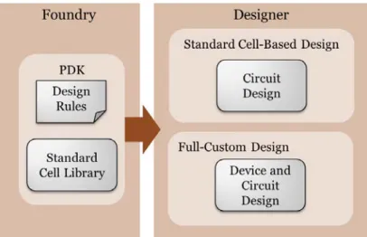
Figure 6 illustrates the workflow of the PDK-oriented design in the foundry-fabless model. In general, the entire design process is divided between foundry and design house. The foundries possess process technology know-how and have developed building blocks (BBs) with known electrical or optical characteristics. The design and support data is handed to designer users in the form of a PDK, based on which designers realize the circuit level design using the BBs directly. In this way, circuit designers are freed from the physics and device level knowledge. In addition, the circuit design task is further split into (i) conceptual design, where the schematic design is realized (logical design); and (ii) physical design (implementation), where the layout is performed according to the schematic. This separation of designs at different abstraction levels enables each of the complex tasks to be carried out by focused-skill specialists.
Figure 6. PDK-oriented PIC design workflow in the foundry-fabless model following the same model as that developed in the EIC industry.
23 As in analog EIC design, PIC designers also tend to optimize their design in the most detailed way in certain circumstances. In this kind of full-custom design flow, designers build their design from the very bottom level of defining the photolithographic layers of devices, which is in direct contrast to using the foundry provided building blocks. This methodology is performed in order to gain chip area and to performance improvement; but it comes at the price of significant design task complexity and design cycle time increase. In the full-custom design flow, pre-designed building blocks can also be used. Often, a chip design involves the combination of both approaches (as shown in the flow diagram in Figure 7) according to the different requirements on performance, cost, etc. Both approaches are also applicable to silicon photonics designs.
1.2.4 Review of current integrated design environments
Some of the CAD software tools we have reviewed in section 1.2.1 “CAD tools for photonic designs” also provide a PDK-oriented design methodology and integrated design environments for silicon photonics. An integrated environment is crucial to silicon photonics design, in order to seamlessly manage the design data when designers move back-and-forth between the segregated design stages in the flow. Such design environments include:
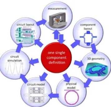
IPKISS/Luceda Photonics [97]
IPKISS provides an integrated design framework as shown in Figure 8. The simulation and design of individual photonic components can be performed and each component can be built into complex circuits. It employs a parametric component design methodology. The components are represented in different views such as mask layout, input/output ports, netlist and S-matrix formalism, and they are respectively used at different design stages. IPKISS manages the design and data flow that covers from device design, circuit design, mask layout and chip measurement. It is scripting-based (Python) and the software can be extended by linking to third-party tools.
Figure 7. The PIC design workflow which combines the standard cell-based design approach using foundry provided pre-characterized building blocks; and the full-custom design approach where the individual layers of the devices and circuits are defined individually by designers.
24 Other similar design frameworks exist and they are implemented through collaborations among commercial photonics tool providers. They have founded a “PDAFlow” organization [98] (where PDA = Photonic Design Automation):
PhoeniX Software [99]
PhoeniX OptoDesigner, together with ASPIC and CleWin, provides a design platform that brings together the simulation, process visualization and mask layout into an integrated design flow (see Figure 9). It is handy to generate a component through the parametric cell approach and create the photonic circuit by placing and connecting the building blocks through its scripting interface. The mask layout tool is hooked up with its electromagnetic simulation tools like the mode solver and beam propagation solver. It supports PDK methodology which provides the user with convenient access to foundry services.
Figure 8. The IPKISS design framework where the design flow is oriented to the definition of single components with different views used for different design stages. [97]
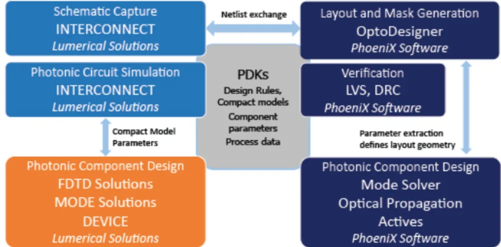
25 PhoeniX Software and Lumerical Solutions [100]
Under the design framework illustrated in Figure 10. , Lumerical's INTERCONNECT [101] provides the schematic capture environment and a photonic circuit simulation tool; and PhoeniX Software's OptoDesigner layout and mask generation module provides the circuit layout and mask fabrication tools. After the schematic is captured and simulated with INTERCONNECT, its netlist can be imported to the OptoDesigner and implemented as mask layout. The completed layout is then exported and the schematic design is updated with the exact component parameters. New simulations can be run in INTERCONNECT to verify if the design still meets the intended performance specifications.
PhoeniX Software and VPIphotonics [102]
Figure 11 illustrates the integrated design flow offered by PhoeniX OptoDesigner and VPIphotonic VPIcomponentMaker which is a circuit design and simulation tool. The flow is demonstrated based on a specific foundry service, and is also PDK-oriented.
Figure 9. The integrated software environment provided by photonic design environment OptoDesigner (Phoenix Software), ASPIC circuit simulator (Filarete), and layout editor Clewin (Wieweb Software). [99]
Figure 10.The photonic design framework for circuit design, simulation and mask layout enabled by INTERCONNECT (Lumerical Solutions) and OptoDesigner (PhoeniX Software). [100]
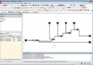
26 IPKISS/Luceda Photonics and Tanner EDA [103],
Tanner is an EDA company that develops a full design tool flow. Its product extends to applications such as analog and mixed-signal circuits, MEMS, and silicon photonics. MEMS design is similar to photonics design in term of its all-angle and curvilinear layout. To deal with the non-Manhattan layout, Tanner’s L-Edit offers powerful editing capabilities, such as defining circles, arc and curves, and component rotation at any angle. By linking the photonics component simulation and design flow of IPKISS to Tanner’s advanced layout editing environment, they provide an integrated PIC design solution.
The above reviewed integrated design flows dedicated to PIC designs are mostly driven by photonics tool providers. A similar design methodology as for EIC is often referred to as photonic design automation (PDA). These tools are specialized in photonic modeling and simulations, so they usually have powerful front-end design capability (like IPKISS, Lumerical and PhoeniX); however, the back-end design flow is usually complemented by bringing in EDA software (like Tanner’s L-Edit) into the flow. In the meantime, there are also efforts from the EDA community to embrace photonics inside existing design platforms. Compared to the PDA flow, the EDA-oriented flow offers several advantages: EDA tool developments have been heavily invested. The EDA methodology is an inseparable part of the CMOS platform – historically, the design is only valid for foundry access if it is performed by using the qualified
Figure 11. The design framework enabled by VPIcomponentMaker (VPIphotonics) and OptoDesigner (PhoeniX Software) for photonic design, simulation and mask layout. [102]
Figure 12. A non-Manhattan photonic layout design realized by Tanner EDA’s L-Edit layout editor. [103]
27 EDA design tools and flows. Reusing mature EDA design flows is more economically viable in terms of cost-saving for tool R&D, and promises better design efficiency and reliability. The automation provided by PDA greatly improves design productivity with integrated design environments. However, its level of maturity and flow integration cannot be compared with the EDA software.
From the EDA point of view, because of the difference between fundamental physics of photonics and electronics, the EDA tools that have been developed for ICs do not lend all of their concepts to the PIC design methodology, especially at the front-end design stage. Bogaert W. et al. [ 104 ] identifies several important aspects where EDA tools are challenged by electronic and photonic co-design problems:
o The information an optical waveguide can carry, and which needs to be analyzed, includes power, phase, wavelength, and mode (or a subset of these parameters depending on the application). It is suggested that there is no straight-forward way of incorporating the richness of photonic signals into a standard electrical circuit simulator; and the better solution is to interface simulators for the electronic and photonic domain. o Photonics design is multi-physics and it involves not only the optical domain, but also temperature, electronic carrier density, and the intrinsic nonlinear optical effect of silicon. The circuit modeling must take all these factors into consideration.
o Waveguide behavior is very sensitive to the actual geometry of the cross section – and thus the process variability. Photonic circuit simulation with process variability can be done with Monte-Carlo, but with many more effects than are covered in electronic design.
Leveraging the EDA framework for photonics design was first demonstrated by Mentor Graphics Pyxis design environment interfaced with photonics software tools [105]. This effort has answered most of the front-end design requests raised previously by introducing the photonic modeling and simulation capability of photonic tools into the EDA framework. The back-end design (physical layout) is also enhanced as compared to classical EDA tool. The physical implementation impact on the photonic circuit behavior is significant, such that it requires careful validation and sometimes needs to be taken care of in early design stages.
Mentor Graphics Pyxis [105]
Mentor Graphics Pyxis is an IC design platform. It offers a mainstream EDA design environment linked to photonic simulation software provided by Lumerical and PhoeniX to create a unified design flow for silicon photonics (Figure 13).
28 Users can capture a photonic design and testbench, set up optical simulation parameters for circuit analysis and simulation. Time-domain and frequency-domain simulations are run using the INTERCONNECT simulators and results are delivered for analysis to the EZwave viewer. Simulation on electrical parts of the circuit is done with the integrated Eldo (general purpose analog simulation) and Questa ADMS simulator (analog-digital mixed-signal simulation). Alternatively, photonic components can also be modeled in Verilog-A [85], so that photonic and electronic circuit can be simulated simultaneously with the Eldo SPICE simulator.
After the schematic is created and validated by simulation and rule check, the layout is implemented interactively with Pyxis Layout. Schematic-driven layout enables users to quickly place and assemble photonic pCells using connectivity-driven waveguide routing with radial and adiabatic bends, as well as S-bend support. During this stage, OptoDesigner implements the layout of photonics building blocks with specified optical behavior. To complete this full-flow silicon photonics design methodology, Calibre tools perform DRC, LVS, lithography simulation, and smart-fill, ensuring that photonic components meet the design intent through the manufacturing process. The result of physical extraction is fed back into circuit simulation to predict the impact of the physical layout. During the schematic and layout design stage, it is possible that designers need to go through the loops several times if the simulation or verification results do not satisfy design specifications. The design flow is also PDK-oriented, which contains the technology-specific data such as electronic and photonic building block and pCell libraries, simulation models, technology information and design rules.
The described flow benefits from photonic CAD software dedicated to photonic simulation, and EDA software which has a clear focus on CMOS technology and complete flow offering. With proper interfaces and data flow management, established between photonic tools and EDA tools, the goal is to achieve a full design automation flow. Other efforts to leverage EDA design tools for photonic include [106][107], which demonstrates Cadence Virtuoso based design flow, however, without integration capability with photonics simulation tools.
Figure 13. The unified design flow through collaboration of EDA (Mentor Graphics Pyxis) and photonic CAD tool providers (Lumerical Solutions and PhoeniX Software). [105]
29 Most testcases in this study are created with the Pyxis platform. The AMPLE scripting interface makes the software manipulation powerful and flexible; and creating complex photonic structures and testcase is also made easy by batch processing with the scripts. We also use this environment as the testbench for physical verification flow development, using its close links to physical verification tools such as Calibre DRC and LVS.
The on-going and future area of study for PIC design tools is to deal with more integrated systems at higher levels of design – i.e. inter-chip or intra-chip optical links. The concept of integrating photonic circuits in EIC was primarily proposed to solve data traffic issues in large scale EIC designs using on-chip optical links; while this is still a potential long-term objective, the most successful applications today of silicon photonics are off-chip optical links used in datacenters for longer reach data link components. There are a large number of on-going studies that explore moving photonics closer to the electronics parts, in which the complexity is much higher. Recently, there have been successful demonstrations of inter-chip optical links [108] with integration scenarios like 2.5D (silicon photonics interposer) [71] and 3D stacks [109]. Another recent publication from C. Sun et al. [110] demonstrates a single electronic-photonic chip, with electronic logic and memory parts and photonic circuits that allows communication with other chips. Optical links for intra-chip systems is even more challenging but various concepts have been proposed for a long time [111][112]. These on-chip optical link systems are larger in scale, which requires a high-level design capability of software tools – system simulation, synthesis, P&R and optimization, and verification (design flow diagram shown in Figure 14), as reviewed in section 1.2.1 “CAD tools for photonic designs”.
Such design tools are not the current market’s most urgent need, since these technologies are still in the research and prototype demonstration phase. However, as the technology evolves, it will drive the need for industry-level design tools. The CAD tools mentioned in section 1.2.1 “CAD tools for photonic designs” provide integrated design environments which are able to realize design driven by system specifications down to the physical level [94][95], and they are essential to prove the benefits of the silicon photonics technology by giving virtual but realistic predictions of the system behavior. They are good examples and potentially worth the effort to integrate these tools with existing EDA design frameworks to leverage its mature technology integration for wider industry adoption.
1.3 The PV Methodology
Figure 14. Realization of complex PIC designs like a Network on Chip system in a top-down approach with an automated design flow.