HAL Id: cea-01791239
https://hal-cea.archives-ouvertes.fr/cea-01791239
Submitted on 19 Feb 2019HAL is a multi-disciplinary open access archive for the deposit and dissemination of sci-entific research documents, whether they are pub-lished or not. The documents may come from teaching and research institutions in France or abroad, or from public or private research centers.
L’archive ouverte pluridisciplinaire HAL, est destinée au dépôt et à la diffusion de documents scientifiques de niveau recherche, publiés ou non, émanant des établissements d’enseignement et de recherche français ou étrangers, des laboratoires publics ou privés.
ZnO nanowires as effective luminescent sensing
materials for nitroaromatic derivatives
Roy Aad, Vesna Simic, Loïc Le Cunff, Licinio Rocha, Vincent Sallet, Corinne
Sartel, Alain Lusson, Christophe Couteau, Gilles Lerondel
To cite this version:
Roy Aad, Vesna Simic, Loïc Le Cunff, Licinio Rocha, Vincent Sallet, et al.. ZnO nanowires as effective luminescent sensing materials for nitroaromatic derivatives. Nanoscale, Royal Society of Chemistry, 2013, 5, pp.9176. �10.1039/C3NR02416D�. �cea-01791239�
ZnO as an effective fluorescence sensor for
nitroaromatic derivatives
R. Aad1, V. Simic3, L. O. Le Cunff1, L. Rocha3, V. Sallet2, C. Sartel2, A. Lusson2, C. Couteau1,
and G. Lerondel1
1 Laboratoire de Nanotechnologie et d’Instrumentation Optique, Institut Charles Delaunay,
CNRS UMR 6279, Université de Technologie de Troyes, 12 rue Marie Curie, BP 2060, 10010 Troyes Cedex, France.
2 Groupe d'Etude de la Matière Condensée (GEMAC), CNRS-UVSQ, 45 avenue des
Etats-Unis, 78035 Versailles Cedex, France.
3 CEA, LIST, Laboratoire Capteurs et Architectures Electroniques, F-91191 Gif-sur-Yvette
Cedex, France
We report room temperature photoluminescence (PL) quenching on ZnO thin film and nanowires in the presence of 2,4-dinitrotoluene (DNT) vapors and for concentration as low as 180 ppb. While ZnO thin film presents a small change in the PL intensity, ZnO nanowires exhibit a strong (95%) and fast (41s) quenching of the PL intensity in the presence of DNT vapor. As shown by calculations, the enhanced ZnO nanowires response can be accounted for by the sample geometry and a better crystal quality. The results demonstrate the importance of nanostructures in improving the sensitivity of ZnO. The study also reveals the sensing capability of ZnO nanowires and paves the path towards the potential realization of low-cost sub-ppb nitroaromatic derivatives sensors.
Introduction
Selective ultra-trace detection of gas analytes is a central challenge in the field of sensors. Current research aims at improving the performances of existing devices [1] (reducing 20 sensitivity threshold, improving selectivity) but also to propose new technological solutions to be able to answer to new needs.
For instance, in the case of explosive detection, there are a number of equipments that have proved their worth (e.g. ion mobility spectrometry, mass spectrometry and gas 25 chromatography) but remain rather bulky, expensive and time consuming procedures. Because of these limitations, research focuses on the development of miniaturized sensors that are sufficiently sensitive, selective, inexpensive and compatible with mass production and wide deployment. In this context, 30 nanostructured metal oxide semiconductors are subject to intense studies for sensing applications [2-4]. In particular, zinc oxide (ZnO) nanostructures have been extensively investigated as active materials for toxic gas detection [5]. Due to their particular geometrical (high surface-to-volume ratio) and physical 35 properties, significant improvements in sensor performances (higher sensitivity and faster response time) have been already observed.
The transducing methods that are generally used to detect the presence of chemical vapours consist of monitoring the changes 40 in the electric or piezoelectric properties of ZnO [6]. Moreover, optical based systems which involve coupling with the m-line and the surface plasmon resonance were also addressed and investigated [7, 8]. However, the direct impact of gases on ZnO luminescence was never considered and studied, until recently 45 [9]. This last approach is one of the most promising due to its inherently very high sensitivity and miniaturization capability, as demonstrated for several polymer sensors [10-12]. The reported results on the fluorescence quenching of ZnO nanostructures in the presence of volatile organic compounds exhibited ppm level 50 detection [13-15], which proved the potentials of
this approach for sensing applications and boosted the motivations towards further nanostructuring challenges and experimental investigations. Some examples have been already reported with systems involving polymeric materials coated onto optically 55 passive nanostructures [16, 17]. While ZnO may not be inherently selective compared to polymers, the use of ZnO nanostructure arrays bearing different functional group influencing the adsorption process may offer a solution to this problem [18]. ZnO presents also other advantages since it is less 60 prone to photodegradation that might compromise long-term stability and durability, unlike polymers [19].
In this article, we report on the photoluminescence (PL) quenching of ZnO thin film and nanowires in the presence of 2,4-dinitrotoluene (DNT) vapour. The PL quenching of ZnO in the 65 presence of nitroaromatic derivatives has never yet been reported.
Compared to the ZnO thin layer, ZnO nanowires are found to exhibit a fast response time and high quenching efficiency when exposed to DNT. This behaviour can be attributed to the higher surface-to-volume ratio, which characterizes the ZnO nanowires 70 geometry. DNT is a predominant vapour signature found in military grade TNT [20]. Thus, ZnO nanowires are investigated as fluorescent sensitive structures for sub-ppm TNT detection.
Experiment
The PL quenching of two ZnO geometries is investigated. The first geometry consists of a 170 nm thick ZnO film (S0), while the second is formed of ZnO nanowires (S1). The thin film and nanowires samples are grown by metalorganic chemical vapor deposition in a horizontal reactor operating at a reduced pressure of 65 mbar on R- and A- sapphire substrates respectively. The substrate holder (graphite covered with SiC) can be heated up to 1000°C using RF induction. Diethylzinc (DEZn) and nitrous oxide (N2O) were used as zinc and
grown at a temperature of 950°C and using a high oxygen/zinc molar ratio, above 14000, in order to favor 2D growth and smooth surface morphology. On the other hand, the ZnO nanowires were grown at a temperature of 875°C and using an oxygen/zinc molar ratio of 940, in order to insure the formation of vertically aligned nanowires with high aspect ratio.
Results and discussion
Figure 1 presents a SEM image of the studied ZnO nanowires. This sample (S1) displays vertically aligned nanowires with a mean diameter of 130 nm and an average length of 3µm. The high aspect ratio of the S1 structures is hoped to enhance the quenching response of the ZnO material. Figure 1 also reveals the presence of a ZnO wetting layer that is inherently formed during the growth of the ZnO nanowires, as already reported [21-23].
Figure 2 shows an image of the experimental setup that was used to investigate the PL response of the two ZnO samples. As seen in figure 2, the ZnO samples are first inserted into a quartz suprasil cell containing DNT crystals purchased from Fluka (analytical grade standard). At room temperature the DNT crystals produce a saturated vapor pressure of 160.10-3 Pa, corresponding to an equilibrium vapor concentration of 180 ppb inside the quartz
cell [24]. After the insertion, the PL spectrum of the two samples is measured at various time delays using a fluorospectrometer equipped with a 450W xenon lamp. Fluorescence spectra are measured from a wavelength of 350 nm to 600 nm, while the excitation wavelength is set to 335 nm. A bandpass filter around 335nm is placed in front of the xenon lamp aperture to insure a monochromatic excitation of the ZnO samples.
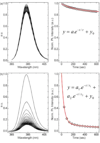
Figure 3 shows the evolution over time of the PL spectrum of the two studied samples, in the presence of DNT vapor (left graphs). The PL spectra presented in Figures 3(a) and 3(b) are each normalized by the corresponding highest PL intensity at the maximum emission wavelength ( max
em
with a max
em
λ at 383 nm, which is attributed to ZnO related near-band-edge emission. Most
importantly, Figure 3 reveals a decrease of the PL intensity of the S0 and S1 luminescence due to their exposure to DNT vapor. The PL quenching of ZnO can be attributed to the adsorption of the nitrogen dioxide (NO2) functions existing in the DNT molecules. NO2
molecules are known to adsorb to the ZnO contact surface (i.e. ZnO/Air interface) through several possible adsorption processes, which involve the trapping of ZnO electrons as explained in [25, 26]. The electron trapping thus decreases the number of the ZnO charge-carriers (e.g. excitons) that can radiatively recombine. As a consequence, the NO2 adsorption
process on the ZnO surface induces a quenching of the ZnO PL intensity. The quenching process is obviously strongly related to the diffusion length of the photo-generated charge carrier in ZnO and their ability to reach the ZnO contact surface. While the two samples exhibit PL quenching, they do not present a similar PL quenching efficiency. The ZnO thin film (S0) spectrum presented in Figure 3(a) displays a very weak, but nonetheless visible, luminescence quenching. On the other hand, in the case of the ZnO nanowires (S1), a remarkable strong and fast decrease of the PL intensity is observed. To quantify the quenching response, the evolution of the max
em
λ intensity of S0 and S1 as a function of time t is
respectively plotted to the right of Figures 3(a) and 3(b). The decrease of the max
em
λ intensity
(black circles) is afterwards fitted using exponential decay equations in order to determine the various quenching parameters. The experimental procedure did not allow the measurement of the PL spectrum and subsequently the max
em
λ intensity, at t = 0s. Therefore, the experimental
data (black circles) were normalized by the extrapolated value of the max
em
λ intensity at t = 0s,
in order to have the max
em
λ intensity at t = 0 equal to 1 (i.e. 100%). Concerning the ZnO thin
film (S0), the PL quenching response is well described by a first-order exponential decay (cf. Table 1), as shown by the fit (red line) in Figure 3(a). The fit parameters of the exponential
decay (cf. Table 1) deduce a mean life time (τ ) of 290 seconds and a quenching efficiency
(QE=1 y− 0) of 15% for the S0 quenching response. On the other hand, the S1 (nanowires) quenching response, could not be correctly fitted with a first-order but a second-order exponential decay (cf. Table 1). The later speculates two distinct PL quenching processes. The fitting parameters (cf. Table 1) reveal a first (fast) process with a mean half time (
τ
1) of41 seconds and a second (slow) process characterized by a mean half time (
τ
2) of 414seconds. The two quenching processes can be explained by the presence of the ZnO nanowires and a ZnO wetting layer in the S1 structure (as seen in Figure 1). S1 effectively presents a fast response time of the order of
τ
1 resulting from the fast quenching process,which is responsible for 85% (a1 =0.85) of the overall PL intensity quenching. In addition to
the fast response, S1 exhibited a very efficient quenching as 95% (QE=1 y− 0) of the overall
luminescence is killed. Eventually, while the ZnO thin film response is deficient for TNT detection, nanowires already appear highly suitable for the realization of a low-cost and sub-ppm TNT sensor working at room temperature. The colossal improvement in the quenching response observed between S0 and S1 strongly suggests a geometrical effect. As already mentioned, the luminescence quenching results from an adsorption process of DNT (trapper) molecules to the ZnO surface and thus, is directly related to the probability of the photogenerated charge-carrier to diffuse and eventually reach the contact surface in order for them to be trapped. Effectively, in the case of S0, the weak quenching response is somehow expected, since such bulky materials logically present low probabilities for a charge-carrier to reach the contact surface. The increase of the surface/volume ratio in case of nanostructures insures a large contact area between the DNT and the ZnO nanowires along with a limited nanowires volume (i.e. stronger charge-carrier space confinement) that should insure an improved probability for charge-carriers to reach the ZnO contact surface. As a consequence,
for ZnO nanostructures, such as S1, enhanced trapping of electrons by the DNT molecules is expected thus increasing the ZnO sensitivity
Table 1. Equations and Fit parameters for S0 and S1.
S0 S1 Equation y=a.e−tτ +y0 0 2 1.e 1 a .e 2 y a y= −tτ + −tτ + Fit parameters 290 =
τ
τ
1=41τ
2 =414 15 . 0 = a a1=0.85 a2 =0.1 85 . 0 0 = y y0 =0.05Monte-Carlo simulations have been realized in order to show the influence of the geometrical factor on the electron trapping (i.e. the quenching efficiency) in the studied ZnO samples. The simulations compute the probability for photo-generated charge-carriers to reach the ZnO/air interface, and therefore be quenched.
The method consists in computing a large number of random-walks for the ZnO charge-carriers as illustrated in Fig 4(a) (right)inset. The charge-carriers are dispersed along the whole volume of the ZnO structures. Since the carriers are photo-generated, their distribution is of course highly dependent on the local optical excitation density. To account for the optical absorption, an exponential decay expression, similar to the Beer-Lambert law, was applied to describe the number of photo-generated carriers in the ZnO thin film and nanowires. The carrier distribution (ne) is given by ne =e−αd, where α is the ZnO absorption
coefficient at the excitation wavelength (α ~ 15 µm-1 at 325 nm) and d is the distance which
separates the carrier from the ZnO/air interfaces. This implies that there are more carriers generated near the ZnO surface rather than deep inside the ZnO structures. This exponential decrease is uni-dimensional for the thin film since the ZnO/air interface is a plane; meanwhile, the decrease is radial for the nanowires with more photo-generated carriers near the borders of the nanowire and fewer close to its center [Fig 4(a) right].
The Monte-Carlo method considers the case of elastic collisions. Thus, two parameters are accounted for to generate the random walks, the mean free path (l) and the diffusion
length (L). The mean free path defines the distance traveled by the carrier between two successive impacts. The diffusion length defines the maximum distance that carriers can travel before recombining, and therefore the maximum number (N = L/l) of steps in a single
walk. The basic principle of the method is to evaluate the probability (Pe) for a carrier
generated at a specific point in the ZnO structure to reach the surface [Fig4(a) right]. Pe is
evaluated over 100 randomly generated diffusion paths and is obtained through the ratio between the number of paths which lead to the ZnO surface within N walks and the total number of generated paths. The probabilities Pe are then weighted by the carrier distribution
[Fig4(b) inset] and the overall probability for the carrier to reach the surface is obtained by
∑
∑
= d e d e e d n d P d n P ) ( ) ( ) (. The Monte-Carlo simulations account for the 3D geometry of the ZnO
structures. Under moderate pumping optical densities, the photogenerated charge-carriers in ZnO exist as excitons. At room temperature, free excitons usually dominate considering the localization energies [27]. Figure 4 presents the results obtained by the Monte-Carlo simulation for the thin film (a) and the nanowires (b). The Figure shows the evolution of the probability for a carrier to reach the surface as a function of the diffusion length and for various mean free paths. As seen in Figure 4, the increase of the exciton diffusion length, as well as the increase of the mean free path, increases the probability for the exciton to reach the surface, in the case of the thin film and the nanowires. Nonetheless, the Monte-Carlo simulation clearly shows the influence of the geometry on the quenching efficiency. As shown in Figure 4, the nanowires always exhibit a higher probability for the excitons to reach the surface than the thin film. In addition, the calculated probability for the thin film [Fig 4(a)] shows a graduate increase with the diffusion length and the mean free path. For the highest
value of the diffusion length and the mean free path (i.e. L = 2000 nm and l = 100 nm), the
probability for the excitons to reach the thin film surface is however less than 100%. On the other hand, the calculated probability for the nanowires [Fig 4(b)] shows a strong and sharp increase with the diffusion length and the mean free path. The probability for the excitons to reach the nanowires surface is nearly 100% for a diffusion length of 1000 nm and a mean free path of 20 nm.
The experimentally observed quenching efficiencies for the thin film (15%) and the nanowires (95%) can be interpreted with various values of the diffusion length and the mean free path. However the diffusion length (l) of free excitons in ZnO thin films is reported to
be between 100 and 200 nm at low temperatures [28-30]. Moreover, recent experimental studies have also showed that free excitons of ZnO nanowires possess diffusion lengths around 150 to 200 nm, also realized at low temperatures (5~8 K) [31, 32]. The diffusion length of free excitons is a parameter mainly related to the nature of the material itself (i.e. ZnO), what explains the similar diffusion lengths observed in thin films and nanowires. However, the mean free path is mostly related to the density of defects in the material and therefore the growth quality. Considering a similar diffusion length of 200 nm for the ZnO, the quenching efficiency of the thin film (i.e. 15%) and the nanowires (i.e. 95%) can be respectively explained by a mean free path of ~5 nm and ~100 nm, as shown in Figure 4. The relatively low diffusion length in the case of the thin film can be explained by a higher stacking fault density for epitaxial thin film grown on R - sapphire substrate as compared with sample grown on A- sapphire [33].
The developed model clearly reveals the important impact of the ZnO geometry on the probability for electrons to reach the ZnO/air interface. Assuming that the sample morphology is known, it also points out the effect of the crystal quality (i.e. mean free path) in the quenching probability. It is worth pointing here the benefit of higher crystal quality in
semiconductor materials as compared with organic materials. While the geometrical model developed here was found to give a sufficient insight in the quenching mechanism, further experimental investigations will be necessary to determine the diffusion lengths of the excitons in ZnO at room-temperature. Another aspect lies in the DNT molecules concentration at the interface. While it is usually admitted that the quenching efficiency is limited by the probablility of the photogenerated carriers to reach the surface it can also be limited in the case of ultralow concentration by the density of adsorbed DNT of the ZnO surface. For that respect, the nanometric dimension as well as the high surface-to-volume ratio of the nanowires offer better condition for the DNT adsorption.
Conclusion
To conclude, a quenching phenomenon was observed for ZnO thin film and ZnO nanowires in the presence of DNT vapor. The ZnO thin film is characterized by a slow response time (290 sec) and a low quenching efficiency (15%). On the other hand, ZnO nanowires exhibited improved quenching properties with a fast response time (41 sec) and a high quenching efficiency (95%). The colossal improvement in the ZnO quenching response is attributed to the geometry of the nanowires, which allows for a better trapping of electron by the DNT. This attribution was further confirmed by geometrical calculations taking into account the diffusion length and the mean free path of the excitons in the materials. This study clearly demonstrates once more the importance of inorganic luminescent nanostructured material for sensing applications and paves the path towards the realization of efficient low-cost sub-ppm TNT detectors.
Acknowledgement. This work has been supported by the French National Agency (ANR) in
the frame of its Programme BLANC (ANR-08-BLAN-0296, ULTRAFLU project) and the
Champagne-Ardenne Regional council.
References
[1] J. S. Caygill, F. Davis and S. P. J. Higson, Talanta 88, 14 (2012).
[2] D. Spitzer, T. Cottineau, N. Piazzon, S. Josset, F. Schnell, S. N. Pronkin, E. R. Savinova and V. Keller, Angew. Chem. Int. Ed. 51, 5334 (2012).
[3] G. S. Aluri, A. Motayed, A. V. Davydov, V. P. Oleshko, K. A. Bertness, N. A. Sanford and M. V. Rao, Nanotechnology 22, 295503 (2011).
[4] A. Yildirim, H. Acar, T. S. Erkal, M. Bayindir, and M. O. Guler, , ACS Appl. Mater. Interfaces 3, 4159 (2011).
[5] A. Wei, L. Pan, and W. Huang, Materials Science and Engineering B 176, 1409 (2011).
[6] M. Penza, P. Aversa, G. Cassano, W. Wlodarski, K. Kalantar-Zadeh, Sensors and Actuators B: Chemical 127, 168 (2007).
[7] T. Mazingue, L. Escoubas, L. Spalluto, F. Flory, P. Jacquouton, A. Perrone, E. Kaminska, A. Piotrowska, I. Mihailescu, and P. Atanasov, Appl. Optics 45 1425 (2006)
[8] W.-Y. Feng, N.-F. Chiu, H.-H. Lu, H.-C. Shih, D. Yang, and C.-W. Lin, 30th Annual International IEEE EMBS Conference, 5757 (2008).
[9] D. Valerinia, A. Cretì, A.P. Caricato, M. Lomascolo, R. Rella, and M. Martino, Sensors and Actuators B: Chemical 145, 167 (2010).
[10] J.-S. Yang and T. M. Swager, J. Am. Chem. Soc. 120, 5321 (1998).
[11] J. Li, C. E. Kending, and E. E. Nesterov, J. Am. Chem. Soc. 129, 15911 (2007).
[12] H. Sohn, M. J. Sailor, D. Magde, and W. C. Trogler, J. Am. Chem. Soc. 125, 3821
[13] D. Valerini, A. Cretì, A. P. Caricato, M. Lomascolo, R. Rella, and M. Martino, Sensors and Actuators B: Chemical 145, 167 (2010).
[14] C. Baratto, S. Todros, G. Faglia, E. Comini, G. Sberveglieri, S. Lettieri, L. Santamaria, and P. Maddalena, Sensors and Actuators B: Chemical 140, 461 (2009).
[15] M.C. Carotta, A. Cervi, V. di Natale, S. Gherardi, A. Giberti, V. Guidi, D. Puzzovio, B. Vendemiati, G. Martinelli, M. Sacerdoti, D. Calestani, A. Zappettini, M. Zha, and L. Zanotti, Sensors and Actuators B: Chemical 137, 164 (2009).
[16] A. Rose, Z. Zhu, C. F. Madigan, T. M. Swager and V. Bulovic, Nature 434, 876 (2005)
[17] D. Zhu, Q. He, H. Cao, J. Cheng, S. Feng, Y. Xu and T. Lin, Appl. Phys. Lett. 93, 261909 (2008).
[18] X. Fang, L. Hu, C. Ye and L. Zhang, Pure Appl. Chem. 82, 2185 (2010)
[19] F. W. D. Rost, «Photobleaching, photoactivation, and quenching in Quantitative
Fluorescence Microscopy», Cambridge University Press: New York, 115-127 (1991).
[20] V. George, T.F. Jenkins, D.C. Leggett, J. H. Cragin, J. Phelan, J. Oxley and J. Pennington, Proc. SPIE 3710, 258 (1999).
[21] G. Perillat-Merceroz, P.-H. Jouneau, G. Feuillet, R. Thierry, M. Rosina, and P. Ferret, Journal of Physics: Conference Series 209, 1 (2010).
[22] W. I. Park, D. H. Kim, S.-W. Jung, and Gyu-Chul Yi, Appl. Phys. Lett. 80, 4232 (2002).
[23] D. J. Park, J. Y. Lee, D. C. Kim, S. K. Mohanta, and H. K. Cho, Appl. Phys. Lett. 91,
143115 (2007).
[24] C. Lenchitz and R. W. Velicky, J. Chem. Eng. Data 15, 401 (1970).
[25] A. Bismuto, S. Lettieri, P. Maddalena, C. Baratto, E. Comini, G. Faglia, G. Sberveglieri, and L. Zanotti, J. Opt. A: Pure Appl. Opt. 8, S585 (2006).
[26] J. A. Rodriguez, T. Jirsak, J. Dvorak, S. Sambasivan, and D. Fischer, J. Phys. Chem. B
[27] B. K. Meyer, H. Alves, D. M. Hofmann, W. Kriegseis, D. Forster, F. Bertram, J. Christen, A. Hoffmann, M. Straßburg, M. Dworzak, U. Haboeck, and A. V. Rodina, phys. stat. sol. (b) 241, 231 (2004).
[28] G. Tobin, E. McGlynn, M. O. Henry, and J.-P. Mosnier, Appl. Phys. Lett. 88, 071919
(2006)
[29] M. Addou, J. Ebothé, A. El Hichou, A. Bougrine, J.L. Bubendorff, M. Troyon, Z. Sofiani, M. EL Jouad, K. Bahedi and M. Lamrani, «Cathodoluminescence Properties of Zno
Thin Films», Cathodoluminescence edited by N. Yamamoto (2012).
[30] Z.-M. Liao, H.-C. Wu, Q. Fu, X. Fu, X. Zhu, J. Xu, I. V. Shvets, Z. Zhang, W. Guo, Y. Leprince-Wang, Q. Zhao, X. Wu and D.-P. Yu, Scientific Reports 2, 452 (2012)
[31] J.-S. Hwang, F. Donatini, J. Pernot, R. Thierry, P. Ferret, and L. S. Dang, Nanotechnology 22, 475704 (2011).
[32] J. Yoo, B. Chon, W. Tang, T. Joo, L. S. Dang, and G.-C. Yi, Appl. Phys. Lett. 100,
223103 (2012).
FIGURE CAPTIONS
Figure 1. SEM images of ZnO nanowires deposited on sapphire substrate by MOCVD technique.
Figure 2. Picture of the experimental set-up used for fluorescence quenching studies under static conditions.
Figure 3. (a) Evolution of the PL spectrum (to the left) and the max
em
λ intensity (to the right) of
the ZnO thin film (S0) upon exposure to DNT vapor at room temperature. (b) Evolution of the PL spectrum (to the left) and the max
em
λ intensity (to the right) of the ZnO nanowires (S1) upon
exposure to DNT vapor at room temperature.
Figure 4. (a) Probability of exciton reaching the surface of a 170 nm thin film as a function of the diffusion length for various values of the mean free path. (b) Probability of exciton reaching the surface of a nanowires of 130 nm diameter and 2 µm height as a function of the diffusion length for various values of the mean free path. The figure inset shows (to the left) a representative 3D image of a random exciton diffusion path and (to the right) a cartography of the exciton weight and probability distribution at the apex of the nanowire (for symmetry reason only half of the nanowire is represented). Due to the optical absorption, the probability of quenching is higher at the surface of the nanowire.
Figure 3 0 / .e y a y = −t τ + 0 / 2 / 1 2 1 . . y e a e a y t t + + = − − τ τ