HAL Id: hal-03016862
https://hal.archives-ouvertes.fr/hal-03016862
Submitted on 20 Nov 2020
HAL is a multi-disciplinary open access
archive for the deposit and dissemination of
sci-entific research documents, whether they are
pub-lished or not. The documents may come from
teaching and research institutions in France or
abroad, or from public or private research centers.
L’archive ouverte pluridisciplinaire HAL, est
destinée au dépôt et à la diffusion de documents
scientifiques de niveau recherche, publiés ou non,
émanant des établissements d’enseignement et de
recherche français ou étrangers, des laboratoires
publics ou privés.
Characterization of electromagnetic fields of radiating
systems by thermo-fluorescence
Hugo Ragazzo, Daniel Prost, Jean-François Bobo, Stéphane Faure
To cite this version:
Hugo Ragazzo, Daniel Prost, Jean-François Bobo, Stéphane Faure. Characterization of
electromag-netic fields of radiating systems by thermo-fluorescence. 2020 International Symposium on
Elec-tromagnetic Compatibility - EMC EUROPE, Sep 2020, Rome, Italy. pp.1-6,
�10.1109/EMCEU-ROPE48519.2020.9245854�. �hal-03016862�
Characterization of electromagnetic fields of
radiating systems by thermo-fluorescence
Hugo Ragazzo ONERA/DEMR Université de Toulouse F-31055 Toulouse, France hugo.ragazzo@onera.fr Stephane Faure LPCNO INSA F-31055 Toulouse, France s-faure@insa-toulouse.fr Daniel Prost ONERA/DEMR Université de Toulouse F-31055 Toulouse, France daniel.prost@onera.fr Jean-François Bobo CNRS CEMES F-31055 Toulouse, France jfbobo@cemes.frWe choose an alternative way using thermo-sensitive films which had been developed for infrared thermography method called EMIR (ElectroMagnetic InfraRed). Our objective in the present work is to replace IR thermography by thermo-fluorescence spectroscopy; thus we move to visible range, to improve the spatial resolution o f the images.
The film is an electric or magnetic absorbent coated with a thermo-fluorescent layer. In the presence o f an electromagnetic field, the energy absorbed by the film is converted into heat, leading to a variation o f the fluorescence intensity. The variation o f the fluorescence intensity (AFluo) is recorded and post-processed to obtain the incident field. Low frequency modulation o f the RF signal, coupled to synchronous demodulation o f fluorescence signal, permits to cancel the conduction and convection phenomena that would degrade the field visualization.
II. GENERAL PRINCIPLES
A. Experimental Set-Up
Figure 1 is the schematics o f the EMVI setup [6]. The microwave power is modulated at 0.2 Hz. The film is exposed to green LED spot (wavelength: 535 nm). The fluorescence variation is registered by an S-CMOS camera (Dhyana400D 4 Megapixel). The S-CMOS camera is equipped with a low-pass 580 nm filter in order to collect the fluorescence signal.
Microwave source Thermography Signal processing
Figure 1 Thermo-fluorescence imaging setup schematics
Abstract— Characterization of the electromagnetic field emitted by various sources (antenna, radar) is an important issue, either for civil or defense applications. The measurement of the electromagnetic field may be performed by a local probe, the infrared thermography imaging being an alternative way. The latter method, called EMIR [1] (ElectroMagnetic InfraRed) has been used for years at ONERA where it had been developed. We have recently successfully implemented this technique in the domain of visible light, named as EMVI [2] (ElectroMagnetic Visible Imaging). As in EMIR, a thin film (sensitive to either electric field or magnetic field) is heated by the emitted field. But here the film is coated with a polymer doped with fluorescent molecules. As the fluorescent emission depends on the temperature of the film, we achieve a novel thermofluorescent sensor. The results presented here illustrate that new method: both magnetic and electric field imaging of two different radiating systems
Keywords—Electromagnetism, Thermography, Magnetic
losses, Electric losses, Thermo-fluorescence, Meta-material, Zero Order Antenna, High Impedance Surfaces
I. In t r o d u c t io n
We present in this paper a method for electromagnetic field measurement and imaging in visible wavelengths using fluorophore. In a first step we detail the general principles o f this method, then we present measurements o f electric and magnetic near field o f radiating systems.
In electromagnetic compatibility an issue is the measurement o f the electromagnetic field, in particular the near field cartography, to study its interaction with the environment. Strong expansion o f the microwave technologies in our environment can be observed for global civil applications (GPS, communications, phone...) or more specific technologies (remote sensing, aeronautics, medicine ...). Interaction between the microwaves and the surrounding environment thus requires a fast method for imaging and measuring the electromagnetic field.
There are different strategies to characterize the electromagnetic field on a large scale. One is to use electromagnetic probes [3, 4] in matrix or with a scanning system. The main disadvantages are the long acquisition time, the intrusive behavior and the large size o f the scanning system. Another approach, introduced by Hasegawa [5] in 1995, is to use sensitive films.
(
6
)B. Thermo-sensitive thin film s
We use two kinds o f thermo-sensitive films, one sensitive to the electric field and the other sensitive to the magnetic field.
To measure the electric field E, we use a thin film with low-conductivity:<T = 10 to 100 S / m .The film, a Kapton®- type doped with carbon, has a surface impedance:
Zs = — = 2 k C l (1)
Where a (S.m'1) the electric conductivity and e (pm ) the thickness o f the film (e = 50 pm for the Kapton film). The coupling between the electric field and the sensitive thin film generates heat via Joule losses. Under microwave excitation, the Kapton film absorption rate A is related to the surface impedance Zs [7]:
_ 4ZSZ0
(Z0+2ZS)2 (
2
)In our case the absorption rate A is about 15 %, which is large enough to generate a heat variation that is measurable, and weak enough to keep it not intrusive. The density o f absorbed power Pabs (in W.m'3) is related to the electric field by:
Pabs — 2ZS
e(Z0+2Zs)2 (
3
)Pabs is proportional to the square o f the amplitude o f the electric field. As the heating is proportional to Pabs, we have:
|E| = k E^ f g (4) With kE a constant o f proportionality.
To measure the magnetic field H, we use a thin film composed o f ferromagnetic micro-particles embedded in polymer matrix. These films are manufactured by TOKIN Japanese Company [8] for shielding applications. They are electrically insulating and have a good magnetic susceptibility. Depending on the excitation frequency o f the magnetic field, two main losses processes can be invoked: at low frequency (typically dc-1 MHz range), hysteresis losses will be responsible for heating with an effective absorption defined by the SAR (specific absorption rate):
SAR = A. f (5)
With A the area o f the magnetization hysteresis loop (J/g) and f the excitation frequency [9]. Note that A is proportional to the square o f the magnetic field amplitude in the low magnetic field regime.
At larger excitation frequency (0.1 to 10 GHz), in the microwave regime, Ferromagnetic Resonance (FMR) losses or precessional losses will take over hysteresis losses. They are related to the imaginary part o f the permeability o f the ferromagnetic material and the field frequency. Thus the absorbed power Pabs(W.m'3) is proportional to the square o f the magnetic field H:
Pabs = n f \i'H 2
With realistic values o f p" (10 to 100), e (film thickness: 30 to 300 pm), ~ 1 GHz frequency, we end up with a surface absorbed power (e.Pabs) o f several percent o f the excitation power (pqH2/2), therefore compatible with low intrusiveness o f the sensing film.
In summary, the magnetic field amplitude is proportional to the square root o f the observed temperature change:
| f / | =
kHyJ
ATavg (7) With 1cH a constant o f proportionality.C. Thermo-fluorescent Layer
The fluorescence layers are made o f Rhodamine B diluted in ethanol and embedded in epoxy resin. Those layers must fulfill the following characteristics: (i) absorption and emission wavelengths have to be discriminated; this is the case for RhB where the emission wavelength is 580 nm and the absorption wavelength is 555 nm. (ii) The fluorescence must depend on temperature; for RhB we have a variation o f the quantum yield proportional to the temperature variation, with fluorophore sensitivity o f 2 %/K (and this variation is linear from 273 to 393K [10]). (iii) The thickness o f the layer must remain below the thermal diffusion length D. We assume that we are in the case o f thin film that simplifies the heat equation in 2D:
t < D(fmod)
(8)
With t the thickness o f the film (including the fluorescent coating) and D (/mod) the thermal diffusion length, which depends on the modulation frequency f mod. In our case
D(fmod) = 50 to 500 pm, f o r 1 to 0.1 Hz, and t= 80 pm (Kapton + RhB) or t = 60 pm (Tokin + RhB).
D. Lock-in thermography
We use a lock-in thermography technique [11, 12] to increase the signal to noise ratio o f the measurement. This technique permits to avoid continuous thermal effects like natural convection. The microwave power is modulated and the evolution o f the temperature can be written as (See Figure
2
):
T(t) = Tenv + ATavgmod ( l -
e"G D )
+
n(fmod, cp) (9)
With A T ^ and 0 the peak to peak amplitude and phase angle o f a square function
n(fmod)
o f a duty cycle fmod.Figure 2 TOKIN-film heating evolution under constant (dotted green line) and 0.2 Hz modulated (blue line) magnetic excitation [6]
capacitors, in order to avoid vias. It is difficult to make measurements on such system because of its small size.
Figure 4 Zero order antenna schematics
We want to extract ATmod. A good approximation is
A Tmod = -,PabsB (10)
^ 4h2 + (pCp e o>)
B. Images o f electric and magnetic field o f ZOR antenna Images of the electric and magnetic near fields emitted by the ZOR antenna have been achieved. For the measurements, the sensitive films were placed at 2 mm and the microwave frequency was 4.29 GHz.
With Pabs, h the heat transfer coefficient ~10 W.m"2.K_1 for natural convection), p the conductivity and Cp the heat capacity.
The modulated signal of fluorescence is proportional to the heat. For example, Figure 3 shows the evolution of the signal o f one pixel o f the camera. Applying a fast Fourier transform algorithm, we obtain the mean AFluo on each pixel and therefore the ATmod [13]. Then, E or H amplitude can be deduced from (4) and (7) respectively.
Figure 3 Evolution of fluorescence under 0.2 Hz modulated magnetic excitation
III. ZERO ORDER ANTENNA (ZOR) A. Introduction
A zero order antenna is made of capacitor and inductor elements which are swapped on the transmission line (See Figure 4) [14]. Microstrips were etched onto a 0.762 mm thick Cu-clad Arlon substrate, with a relative permittivity of 2.55. The spatial period was 2.5 mm, and the line width was about 1.5 mm. We chose interdigitated capacitors to get the series lumped elements, made of eight 100 pm-separated strips, with a surface o f about 1.5 mm x 2 mm. The shunt inductances were 100 pm wide and 13.5 mm long meander lines. They were connected to 2 mm x 4.8 mm ground
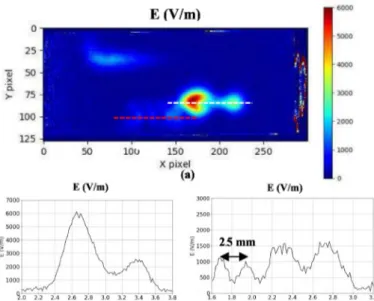
In Figure 5 we present an image o f the electric field (V/m) with kE =603 (4). The microwave power is 37 dBm (around 8 W). Figure 5 (b) reveals a main emission lobe and Figure 5 (c) secondary lobes. On secondary lobes we can observe the spatial period of the periodic elements of the ZOR. The electric emission is due to the capacitor elements (see Figure 4). In Figure 5 we can observe that the electric field patterns are localized on the capacitor elements.
Figure 5 (a) Image of electric field of ZOR antenna at 4.29 GHz, (b) profile of the f t iin lobe (white dotted), (c) profile o fth e secondary
lobes (red dotted)
Figure 6 represents the square root of ATmod, therefore proportional to the magnetic field (7). We thus obtain magnetic field image and profile. The microwave power is 38 dBm (around 6 W). Figure 6 also reveals a main emission lobe and secondary lobes. On the secondary lobes we observe the spatial period of the periodic capacitor and inductor elements. As the magnetic emission is due to the
inductor elements, we can observe in Figure 6 the magnetic near field pattern localized on those elements.
elements. We can simply model HIS by a LC parallel circuit.
H (a.u)
100
100 125 pixel
Figure 6 (a) Demodulated image of the magnetic field of ZOR antenna at 4.29 GHz, (b) P ^ file (red dotted)
IV. Hig hi m p e d a n c es u r f a c e(HIS)
A. Introduction
HIS is a special passive electromagnetic structure (based on metamaterial technology) designed for reducing mutual coupling between patches antennas (for applications where size constraints are crucial: space systems for example).
(a) (b)
HIS cells Microstrip line
Ground plane
Figure 7 Simulation setup of the HIS embedded in the transmission line and picture of the realized structure [15]
B. Images o f electric field o f HIS
We present in this section images of electric and magnetic field of HIS for a range o f frequencies from 1GHz to 1.8GHz. Figure 8 shows the experimental setup for this measurement.
Figure 8 Experimental setup for the measurement of the magnetic field of the HIS
Figure 9 presents the measured Si2 parameter with and without the film [15]. It can be observed that the band gap frequencies are conserved with the presence of the sensitive- film. So we can conclude that the film is non-intrusive. We can observe two cut-off frequencies at 1.3 GHz and 1.9 GHz (EMVI measurements will therefore be achieved for the first
Figure 9 Si2 measurement of the HIS, with and without the thermo-emissive film [15]
Figure 10 shows the amplitude of the field (V/m) on the H IS line, for different frequencies (from 1 to 1.8 GHzFigure 10):
Figure 7 shows how the HIS cells are located between the ground plane and the transmission line [16]. It is made of periodic elements consisting of two layers dielectric substrate. The first dielectric layer includes a ground plane on the bottom face. The second layer is made of the same material as the first. This layer is printed on its two faces with copper. On the bottom face there are hexagon shape pattern and on the top face, equilateral triangle shape pattern with metallic via to connect the ground plane. The HIS is therefore composed of periodic capacitive and inductive
The Figure 10 exhibits different behaviors o f the HIS depending on the frequency: at passing frequencies (1 GHz for example), the electric field appears along the line ; for a cut-off frequency (at 1.35 GHz), a resolution behavior arises and HIS cells resonate: subwavelength details o f the electric near field are thus exhibited. We can note that visualizing these sub-wavelength details would have been impossible with a local probe.
Figure l l shows the evolution o f the amplitude o f the field at the output side o f the transmission line (corresponding to the red cross - x = 10, y = 60-, on the left o f the Figure 10. We obtain a good agreement with the Si2 measurement presented in Figure 9.
Figure 11 Output electric field on the HIS as a function of the frequency
C. Images o f magnetic fie ld ofH IS
In this section, we present qualitative images o f the magnetic field. Indeed, it was difficult to obtain a quantitative measurement because o f the uncertainty o f the ferromagnetic film properties (that are needed to evaluate the kH factor o f the (7)). Images presented in Figure 12 although represent the square root o f AT,,^, therefore proportional to the magnetic field (7). As previously, we observe a passing behavior at 1.1 GHz and a resonant behavior at 1.3 GHz.
Figure 12 Magnetic field patterns at two frequencies
V . Co n c l u s i o n
In this paper we presented characterization o f two radiating systems using EMVI method. We exhibit complex near field pattern produced by ZOR antenna and HIS metamaterial structure. For ZOR antenna, electric and magnetic field patterns o f the whole structure have been obtained for one frequency and one microwave power. For the HIS structure, electric field patterns have been obtained for a frequency range from 1 GHz to 1.8 GHz (first bandgap regions) and the magnetic field have been obtained for two frequencies (one in bandwidth and one in bandgap regions).
For ZOR antenna, the patterns show the behavior o f the capacitor and inductor periodic elements. For HIS structure the electric patterns show how this structure behaves in the frequency range, more especially in the first bandgap regions. Image o f magnetic field o f HIS show the resonance o f the HIS cells at 1.3 GHz.
We thus show that we can visualize complex near field by thermos-fluorescence. These kinds o f field images are
difficult to obtain by experimental usual methods (EM probes) or even by simulation. In the future we shall be able to distinct the components o f the field, using anisotropic films.
References
[1] P. Levesque, L. Leylekian, “ Capteur vectoriel de champs
électromgnétique p a r thermographie infrarouge ”, French Patent
n°9816079,1998
[2] S. Faure, J.F. Bobo, J. Carrey, F. Issac and D. Prost, “Composant
sensible pour dispositif de mesure de champ électromagnétique p a r thermofluorescence, procédés de mesure et de fabrication correspondants", French Patent, n°1758907,2017
[3] H.I. Bassen, G.S. Smith, “Electric Field Probes", IEEE transactions on antenna and propagation, V 0L .A P -31,N 0.5, September 1983 [4] J. Lenz, A.S. Edelstein,"Magnetic sensors and their applications",
IEEE Sensors Journal, VOL. 6, NO. 3, June 2006
[5] T. Hasegawa, “A new method o f observing electromagnetic fields at
high frequencies by use o f test paper", Bull. Yamagata Univ. IV,
Japan, 1995
[6] S. Faure, J-F. Bobo, D. Prost, F. Issac, and J. Carrey,
"Electromagnetic Field Intensity Imaging by Thermofluorescence in the Visible Range”, Phys. Rev. Applied 11,054084,2019.
[7] D. Prost, F. Issac, F. lemaître and J.P. Parmentier, "Infrared
Thermography o f Microwave Electromagnetic Fields”, International
Symposium on electromagnetic compatibility (EMC EUROPE), 2012 [8] https://www.tokin.com/english/product/pdf_dFflex.pdf
[9] J. Carrey, B. Mehdaoui, and M. Respaud, ” Simple models fo r
dynamic hysteresis loop calculations o f magnetic single-domain nanoparticles: application to magnetic hyperthermia optimization J.
Appl. Phys. 109,083921,2011
[10] J. Lou, T.M. Finegan, P. Mahsen, T.A. Hatton and P.E. Laibinis, "Fluorescence-based thermometry: principles and applications", Dep o f chemical engineering, Massachusetts Institute
o f Technology, Cambridge, MA 02139, USA
[11] S. Huth, O. Breitenstein, A. huher and U. Lambert, "Localization o f
gate oxide integrity defects in silicon metal-oxide-semiconductor structures with lock-in IR thermography",!. Appl. Phys. 88,4000,
2000
[12] G. hreglio, A. Race, L. Maresca, M. Riccio, G. Romano and P. Spirito, "Infrared thermography applied to pow er electron devices
investigation ”, Facta Universitatis, Series: Electronics and energetics
28,205,2015
[13] H. Ragazzo, S. Faure, J. Carrey, F. Issac, D. prost and J.F. Bobo, "Detection and imaging o f magnetic field in the microwave
regime with a combination o f magnetic losses material and thermofluorescence molecules", IEEE Transmagn. 55, 6500104,2019
[14] T. Crépin, F. Issac, D. Prost, and S. Bolioli, "Microwave electric field
imaging o f metamaterials using thermoemissive films", IEEE
Antennas Propag. Mag. 56,37,2014
[15] D. Prost, F. Issac, C. Martel, N. Capet, J. Sokoloff, and O. Pascal,”
Electric firld imaging o f a high impedance surface fo r GNSS array decoupling application”, J. Appl. Phys, 72:11001,2015
[16] N. Capet.,"Amelioration du découplage inter élément p a r surface
haute impédance pour antennes réseaux GNSS compactes",Ph.D.
![Figure 1 is the schematics o f the EMVI setup [6]. The microwave power is modulated at 0.2 Hz](https://thumb-eu.123doks.com/thumbv2/123doknet/13486929.413810/2.892.469.823.844.1046/figure-schematics-emvi-setup-microwave-power-modulated-hz.webp)