The Development of an Innovative Bonding Method for Microfluidic Applications By
Michelle E. Lustrino
Submitted to the Department of Mechanical Engineering in Partial Fulfillment of the Requirements for the Degree of
Master of Science in Mechanical Engineering at the
Massachusetts Institute of Technology June 2011
ARCHIVES
MASSACHUSETTS INSTITUITE OF TECHNOLOGYJUL 2
9
2011
LIBRARIES
© 2011. Massachusetts Institute of Technology. All Rights Reserved.
The author hereby grants to MIT permission to reproduce and to distribute publicly paper and electronic copies of this thesis document in whole or in part in any medium now known or
hereafter created.
Signature of Author ...
. . .t .
6
1i/
Department of Mechanical Engineering February 28, 2011
Certified by ... ....
Accepted by ...
David E. Hardt Professor of Mechanical Engineering Thesis Supervisor
David E. Hardt Professor of Mechanical Engineering Graduate Officer
The Development of an Innovative Bonding Method for Microfluidic Applications By
Michelle E. Lustrino
Submitted to the Department of Mechanical Engineering on February 28, 2011 in Partial Fulfillment of the Requirements for the Degree of
Master of Science in Mechanical Engineering ABSTRACT
The field of microfluidics has powerful applications in low-cost healthcare diagnostics, DNA analysis, and fuel cells, among others. As the field moves towards commercialization, the ability to robustly manufacture these devices at low cost is becoming more important. One of the many challenges in microfluidic manufacturing is the reliable sealing of the microfluidic chips once the channels have been generated.
This work was an investigation of innovative ways to robustly heat the substrate-cover plate interface of a microfluidic device for the purpose of bonding and sealing the microfluidic channels. An extensive literature review revealed the benefits of interfacial heating, and both simulations and experimental investigations were used to evaluate a few different methods. Ultimately, a unique method was established that uses light to provide both the bonding energy and the illumination for an in-process vision system for real-time viewing and control of the bonding process. The process results in the generation of a homogenous and optically clear bond, and preliminary tests show that when properly controlled, a bond with minimal microchannel deformation can be created.
Thesis supervisor: David E. Hardt
Acknowledgements
I would first like to thank Professor David Hardt for an incredible opportunity during both my undergraduate and graduate studies, and for all of his guidance and advice throughout
the research process. His mentorship has been invaluable.
Thank you to the Singapore-MIT Alliance for the funding to make this project and my graduate studies possible.
I would also like to thank the other students in Professor Hardt's lab - Matt Dirckx, Aaron Mazzeo, Melinda Hale, and Joe Petrzelka - whom I have had the pleasure of
collaborating with over the past several years and whom I have learned a lot from. Thank you also to Hayden Taylor for sharing so much of his knowledge about the microfluidic bonding process and previous bonding research with me. And to the [iFac team - Professor Hardt, Dr. Brian Anthony, Melinda Hale, Dean Ljubicic, and Nadege Zarrouati - for always giving me valuable input and advice during IAFac meetings.
Thank you to the LMP machinists, Bill Buckley, Pat McAtamney, and Dave Dow, who were always extremely helpful in my machine shop endeavors over the years. And to Rachel Russel and David Rodriguera for all of their administrative assistance.
My graduate school and research experiences certainly would not have been the same if it weren't for the great atmosphere in 3 5-135, thank you to all of my fellow labmates who made it that way! And thank you to all of my friends who have given me such great memories and endless support throughout my MIT experience.
Last, but certainly not least, I would like to extend a tremendous thank you to my family for making my MIT opportunity possible and supporting me every step of the way. Thank you for always being there for me - it means more than words can say.
Table of contents
A cknow ledgem ents ... 4
Table of contents ... 5
List of figures ... 7
List of Tables... 12
1 Research M otivation... 13
1. 1 Im portance of M icrofluidics... 13
1.2 M anufacturing M icrofluidic D evices ... 14
2 Current M icrofluidic Bonding M ethods... 20
2.1 Bonding Therm oplastics... 20
2.2 A dhesive Bonding ... 20
2.3 Lam ination Film Bonding ... 22
2.4 Therm al Bonding... 22
2.5 Surface M odification... 24
2.6 Solvent A ssisted Bonding ... 25
2.7 Localized W elding ... 26
2.8 Laser W elding of Plastics... 27
2.9 Research D irection ... 28
3 Therm al Bonding and Interface H eating ... 29
3.1 The Therm al Bonding Process ... 29
3.2 Interfacial H eating... 31
3.3 Research Focus... 34
4 Three-Stage N on-Contact Surface Heating ... 35
4.1 G eneral Concept... 35
4.2 H eat Transfer Sim ulations... 36
4.2.1 Sim ulation Setup ... 36
4.2.2 Initial Sim ulations ... 37
4.2.3 M inim izing Convective Losses ... 41
4.2.4 M inim izing conduction losses... 43
4.2.5 Bonding/W elding Stage ... 47
5 H eat A bsorbing Surface Coatings ... 49
5.1 Surface G old N anoparticles... 49
5.2 Selectively A bsorbing Dyes ... 52
5.2.1 O verview ... 52
5.2.2 Basic H eat Transfer Sim ulations... 54
5.2.3 A bsorption Spectrum of PM M A ... 57
5.2.4 Coating Selection ... 58
5.2.5 Investigation of Light Sources: IRED s ... 59
5.2.6 Bonding with the OSRAM Ostar Observation IR Emitter... 63
Prelim inary Experim ents... 66
5.2.7 H eat Transfer Sim ulations of Spot H eating ... 69
5.2.8 Investigating Light Sources: Broadband Light ... 75
Basic Broadband A nalysis... 75
Tem perature M easurem ents ... 79
6.1 Achieving an advantageous temperature gradient while heating with broadband light 87
6.2 Choosing a source of uniform light... 90
6.2.1 Different Light Bulbs ... 90
6.2.2 Fiber Optics ... 92
6.2.3 Integrating Spheres... 93
6.3 Implementing the Integrating Sphere ... 100
6.3.1 Initial Testing ... 100
6.3.2 M easuring the Uniformity of Light Exiting the Sphere ... 101
6.3.3 Monitoring Temperature Profiles Through Thickness of Part During Bonding ... 113
6.4 In-Process Vision System for Bonding with Light ... 120
6.5 In-Process Bonding M easurements ... 128
6.6 M easurement of Channel Deformation ... 132
6.7 Future Developments ... 141
7 Conclusions ... 143
List of figures
Figure 1-1. Microfluidic mixer pattern used in the iFac project... 16
Figure 1-2. Leaks on a microfluidic device due to insufficient bonding. Courtesy of Ali B eyzavi, N T U ... 17
Figure 1-3. Blocked channels on a bonded microfluidic device due to excessive deformation during bonding. Courtesy of Ali, Beyzavi, NTU. ... 18
Figure 2-1. Schematic of interstitial bonding technique [13]... 21
Figure 3-1. Schematic of a conventional thermal bonding setup. The substrate and cover plate are clamped in between two heaters. Both pieces are brought up to a temperature greater than their glass transition temperature and pressure is applied to facilitate bonding across the interface. ... 29
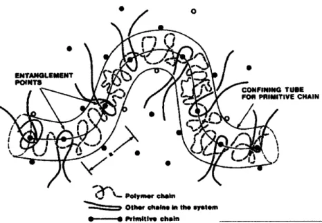
Figure 3-2. Reptation model of interdiffusion. The molecules are described as sliding, or "reptating," through a "tube." The tube contours are defined by the locus of entanglements with neighboring molecules, with the motion of the polymer chains transverse to the contour of the tube severely restricted. [34]... ... ... 30
Figure 3-3. Phases of welding. a) and b) The interface has no mechanical properties and two distinct faces still exist. c) Wetting - intimate contact between the two surfaces has been achieved and potential barriers associated with inhomogeneities at the interface disappear. The molecular chains are free to move across the interface in reptation. Once the reptation time has elapsed, the chain has forgotten its original configuration. [36]... 32
Figure 3-4. Model for temperature dependence of shear modulus. The glass transition temperature of 80*C is specified here for PETG. Model can be used for other Tg's as well. The AO gap is typically 30*C. [37]... 33
Figure 4-1. The basic concept of three-stage, non-contact surface heating. In step 1, the cover plate and substrate are held apart a small distance from one another and a heater heats the surfaces of each. In step 2, the heater is removed and in step 3, pressure is applied to the cover plate-substrate stack in order to promote interfacial diffusion... 35
Figure 4-2. Temperature vs. time for various nodes throughout the thickness of the cover plate during simulation of three-stage heating process. Simulation parameters are those from Table 4-1. The z-values represent the distance of the node from the interface surface... 38
Figure 4-3. Temperature profiles through the thickness of the cover plate between the heating and changeover stages and at the end of the changeover stage for the first three-stage heating simulation. Individual points are specific node measurements; the lines are an interpolation ... 39
Figure 4-4. The temperature profile throughout the thickness of the substrate and cover plate when the two are bonded together; profiles are from stage 3 of the 3-stage bonding process. The bold profile line is the initial temperature profile after stages 1 and 2, using parameters from Table 4-1. Arrows indicate progression of time from 0 to 3 seconds. Each new profile line represents a time step of 0.1 seconds... 40
Figure 5-1. Leister Laser Mask Welding. The parts to be welded are placed under a mask of the desired micropattern. When the curtain of light passes over it, the light is selectively absorbed by the plastic in the pattern of the mask. [48]... 52
Figure 5-2. Transmission curves of PMMA in three cases. [49] ... 53
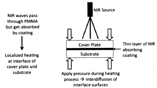
Figure 5-3. Process overview for bonding with an NIR absorbing dye... 54
Figure 5-5. Time for imicron of PMMA surface to reach Tmeit, 160*C, for varying heat fluxes
applied to surface of chip (cover plate or substrate). Determined by finite element
sim u lation s...
55
Figure 5-6. Surface temperature gradients (through thickness of part) at moment when the
temperature at 1 [im deep reached
Tmeit.As determined by finite element analysis for
various applied heat fluxes ...
56
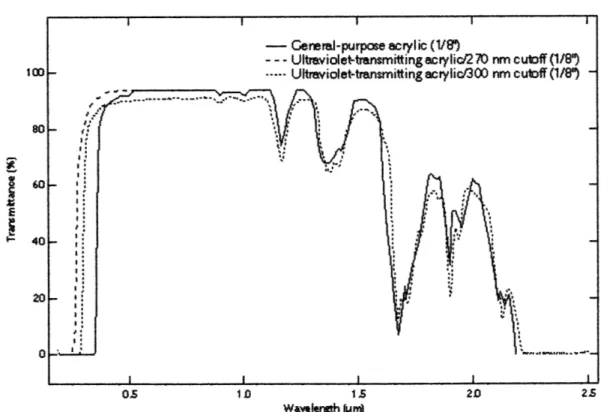
Figure 5-7. The transmission spectrum of 1/8" thick PMMA (acrylic) as reported by Fresnel
Technologies, Inc. [50] The solid line (general purpose acrylic) is the material of interest
for this application...
. 57
Figure 5-8. Absorbance profile of Fabricolor Dye 8472, peak absorption at 848nm. [51]... 59
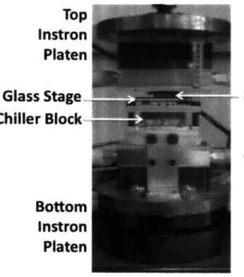
Figure 5-9. Test setup for the OSRAM IR Emitter. The emitter sits on a chiller block for
thermal management. A glass stage is attached to the assembly with magnetic supports on
either side of the emitter for the substrate/cover plate stack to sit on...
64
Figure 5-10. IR Emitter assembly as mounted in the Instron machine...
65
Figure 5-11. Circuit used to isolate driver from AC line [53]... 65Figure 5-12. Electronics box for OSTAR IR emitter assembly. Wires to emitter deliver the
regulated current to the emitter itself. There are two sets of wires to the DAQ; one set is
used to monitor the current and the other receives the TTL timing signal. ...
66
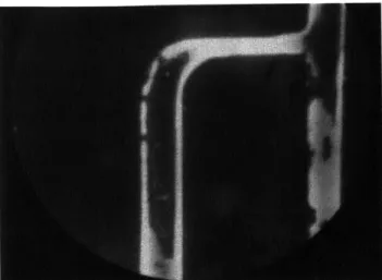
Figure 5-13. Evidence of welding in preliminary experiments with 8472 dye and Osram emitter.
Dye is dissolved in acetone. After welding occurred, the two PMMA pieces were pulled
apart and their surfaces were studied under the microscope. The matching, complementary
contours in these images imply that they were welded...
67
Figure 5-14. PMMA slice used in FEA simulation for spot heating model. A 1* slice was
studied w ith circular sym m etry ...
69
Figure 5-15. Time required for surface to reach
Tmeitfor varying heat fluxes and spot sizes.
Based on FEA simulations. It should be noted that the longer times to melt are
underestimated (described further below)...
70
Figure 5-16. Heat-affected zone for various spot heating conditions. Heat-affected zone is
defined as the thickness through the part that has a temperature greater than T9. The
substrates are 1500 ptm thick; such a heat-affected zone implies the entire substrate is
affected by the heat...
72
Figure 5-17. Emitter chip and fabricolor dye spectra. Emitter chip spectrum from [54] and
Fabricolor dye absorption spectrum from [51]... 73
Figure 5-18. Spectrum of light absorbed by the Fabricolor dye being illuminated by the OSTAR
IR emitter. Found by multiplying the two spectra in Figure 5-17 together... 74
Figure 5-19. Power output profile for a typical 50W, 3000K color temperature halogen light
bulb. Based on blackbody equations ...
76
Figure 5-20. Simple setup to test the bonding with broadband light idea. Light bulbs are MR16
halogen bulbs with aluminized reflectors. Glass is heat-resistant borosilicate. Pressure
w as applied m anually ...
78
Figure 5-21. Simple setup for preliminary broadband heating temperature measurements. ... 80
Figure 5-22. PMMA interface heating by halogen light bulbs...
81
Figure 5-23. Effect of dye type on the temperature trends at the interface during heating by
halogen light bulbs. Dyes are dissolved in a saturated ethanol solution. Blanks are PMMA
pieces with no coating; these are a measure of the pure bulk heating that happens without
the coating. Multiple trendlines of a particular style indicate replicates...
82
Figure 5-24. Effect of dye quantity/concentration on the temperature trends at the interface
during heating by halogen light bulbs. The 8472 dye is used. The acetone solution is at a
high concentration. The ethanol solution is saturated at a low concentration. In the 8472
Ethanol
+
PMMA blank trial, the low concentration ethanol coating is only applied to one
piece of PMMA and the other piece is blank in order to achieve the effect of having less
dye present. Multiple trendlines of a particular style indicate replicates...
83
Figure 5-25. Temperature trends over time for coated and uncoated PMMA pieces, and with and
without light filters. Multiple trendlines of a particular style indicate replicates... 84
Figure 5-26. Temperature trends over time for blanks being heated by broadband light of
different intensities. Intensities are changed by moving the PMMA different distances
from the light bulbs. Multiple trendlines of a particular style indicate replicates... 86
Figure 6-1. Ideal setup for bonding with light idea. A uniform light source sits below a stage
made of IR transparent glass. The substrate is flipped upside down so that the most light is
absorbed at its surface and there is an advantageous temperature gradient through the
channels. Furthermore, since the substrate is inverted, the cover plate can be molten and
will into droop into the channels by gravity...
88
Figure 6-2. Sketch model setup to study active cooling at the backs of the cover plate and
substrate. Channels for chiller fluid surround area where cover plate and substrate stack
w ill be clam ped. ...
. 89
Figure 6-3. Experimental setup for PAR light bulb. The setup is mounted in an Instron machine
so that the Instron can uniformly provide the necessary pressure. The bulb sits below a
stage. The PMMA parts sit on a quartz glass window that is secured in the stage for
greater stiffness against the Instron pressure...
91
Figure 6-4. Picture of an integrating sphere. Light enters through one port, all of the light is
integrated and re-averaged, and uniform light exits another port. ...
94
Figure 6-5. Reflectance curves for Spectralon and Spectraflect, as published by Labsphere [58].
... ... ... ... 97
Figure 6-6. Initial testing for the integrating sphere...
101
Figure 6-7. Setup for light uniformity measurements. The integrating sphere sits within a
supporting structure and the light emitted from the sphere shines through a hole in the
supporting structure, where it can be imaged by the Nikon D90 camera. ... 102
Figure 6-8. Setup for measuring planes outside of the sphere. A) Paper, used as an imaging
surface, is secured to the supporting structure. B) The sphere-paper gap is varied in each
measurement to generate multiple data points. ...
102
Figure 6-9. Setup for measuring planes inside of the sphere. Paper is secured to the back of the
previously fabricated glass holder. The position of the glass holder is varied using shims.
...
103
Figure 6-10. Configuration of output port on integrating sphere. The light exiting the sphere
first passes through the thickness of the Spectralon and then through a short aluminum tube
before exiting the sphere. The planes analyzed here are given distances, 'd', from the
interior of the Spectralon output port. ...
104
Figure 6-11. Centerline across the illuminated area. The color values across this centerline were
used to study the trends in light intensity...
105
Figure 6-12. Plot of color values/intensities across the centerline for each of the RGB color
com ponents...
106
Figure 6-13. Intensity plots across the centerline for the four planes measured outside of the
sphere. C enterline is 1.5" long. ...
107
Figure 6-14. Intensity plots across the centerline for three planes measured inside of the sphere.
C enterline is 1.15" long...
108
Figure 6-15. Average intensity across the centerline compared to distance of the light plane
from the interior of the sphere outlet. This is the distance, 'd, in Figure 6-10 above... 109
Figure 6-16. Standard deviation of light intensity as a function of the distance from the interior
of the sphere outlet. This is the distance, 'd', from Figure 6-10 above... 110
Figure 6-17. Uniformity profile as a function of the distance from the outlet of the Spectralon
portion of the sphere. x/D is the ratio of the distance from the outlet of the sphere
compared to the diameter of the sphere's output port. The d/D ratio is the ratio of the
viewing diameter compared to the actual diameter of the output port. The Ee/Eo
uniformity ratio is the ratio of intensity at the edge of the illuminated area to the intensity
at the center. [58]...
111
Figure 6-18. Intensity variation versus x/D where x/D is the ratio of the distance from the outlet
of the sphere compared to the diameter of the sphere's output port. The sphere's output
port is 1.5" in this case. This trend can be compared to the uniformity trends for d/D
=
0.9
in Figure 6-17 above...
112
Figure 6-19. Light profile of a typical MR16 light bulb at the face of the bulb. ... 113
Figure 6-20. Cross-section of the glass holder setup...
114
Figure 6-21. Temperature trends over time for the three interfaces when 1/8"-thick quartz is
used as the base glass. Multiple trendlines of a particular style indicate replicates... 115
Figure 6-22. Temperature trends over time for the three interfaces when 1/8"-thick borosilicate
is used as the base glass. Multiple trendlines of a particular style indicate replicates. ... 116
Figure 6-23. Temperature trends at the PMMA-PMMA interface for different base glass.
Multiple trendlines of a particular style indicate replicates. ...
117
Figure 6-24. Temperature trends at PMMA-plug interface for different base glass. Multiple
trendlines of a particular style indicate replicates. ...
118
Figure 6-25. Temperature difference between interfaces for different base glass... 119
Figure 6-26. Schematic of the bonding setup in its current state. Light enters the sphere through
an input port. A custom glass holder sits in the exit port and holds the glass base and the
PMMA parts to be bonded. A plug on top of the parts allows uniform pressure to be
applied from a source external to the sphere. In its current state, the light exiting the
sphere passes through the glass and the PMMA parts and certain wavelengths get
absorbed. The plug absorbs the remaining light that is transmitted... 120
Figure 6-27. Schematic of bonding setup with real-time video control. Light exiting the sphere
first passes through the glass and PMMA, and some of it gets absorbed. The light that is
transmitted travels through a glass plug and beamsplitter. At the diagonal midplane of the
beamsplitter, a certain percentage of the light is redirected to the video camera, where a
real-time image of the part being bonded will appear. Uniform pressure can still be
app lied ...
12 1
Figure 6-28. Integrating sphere experimental setup...
122
Figure 6-29. Integrating sphere experimental setup
-
input light configuration... 123
Figure 6-30. Images from bonding video at three different time points. The lighter region is the
area that has been bonded and it spreads out over time. This bonding is done with 1/16"
quartz as the base glass, 0.155MPa of pressure, and three 50W halogen bulbs at the input.
...
12 4
Figure 6-31. Three bonding regions on a microfluidic chip. Region 3 is the area on the chip that
both the PMMA-glass and PMMA-PMMA interfaces. Region 2 is the area on the chip
where bonding has only occurred at one of these two interfaces. The brightness and
contrast have been adjusted to make the different shades more visible...
126
Figure 6-32. Matching contours from bonding video (left) and actual part inspection (right).
Both shades of increased optical clarity indicate region of PMMA-PMMA interfacial
bonding. The outlined region in right image is the bonded region of the device... 127
Figure 6-33. Example of extra bond spreading after lights are turned off but microfluidic chip is
kept under pressure. Image on left is final frame of bonding video, before lights are turned
off. After the lights were turned off, the part remained under pressure for some time and
the bond spread to a region larger than that indicated by the changes in optical clarity from
the video. The outlined region in the right image is the final bonded area of the device. 128
Figure 6-34. Diameter of bonded region over time for parts from two different hot embossing
runs at four different bonding pressures. During the bonding process, three 50W halogen
bulbs were turned on at the sphere's input, 1/16"-thick quartz glass was used as the base
glass, and the fan used to cool the sphere's exterior was kept on. ...
129
Figure 6-35. Diameter of bonded region over time for parts from two different hot embossing
runs at four different bonding pressures. Starting points all normalized to time zero... 130
Figure 6-36. Substrate-cover plate stack. Cover plate area is 0.41 in
2...
...133
Figure 6-37. Channels 1,
5,
and 10 of the serpentine pattern on the microfluidic chip. These are
the channels that are to be m easured...
134
Figure 6-38. Average post-bonding channel heights for channels 1,
5,
and 10, as shown in
Figure 6-37 above. This is the average across nine bonded parts, each of which was
bonded with different input powers and bonding pressures. The error bars are the standard
deviations of the post-bonding heights. Smaller post-bonding heights indicate more
deform ation . ...
135
Figure 6-39. Average post-bonding channel heights and required bonding times for individual
parts bonded with different parameters. Cover plate is that shown in Figure 6-36 above.
The post-bonding channel height is the average of the heights of channels 1,
5,
and 10, as
measured by the Zygo Profilometer. Channel heights are in microns. ...
137
Figure 6-40. Substrate-cover plate stack; smaller cover plate. Cover plate is 0.3in
2in area... 138
Figure 6-41. Average post-bonding channel heights and required bonding times for individual
parts bonded with different parameters. Cover plate is that shown in Figure 6-40 above.
The post-bonding channel height is the average of the heights of channels 1,
5,
and 10, as
m easured by the Zygo Profilom eter. ...
139
List of Tables
Table 3-1. Stages of polymeric diffusion according to the reptation model [34]...30
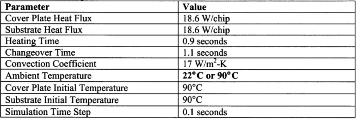
Table 4-1. Heating parameters for initial three-stage heating simulations...37
Table 4-2. Simulation parameters for ambient temperature study. Two simulations were run,
each with different ambient temperatures...
41
Table 4-3. Simulated surface temperatures after heating and changeover stages for varying
am bient tem perature conditions...
41
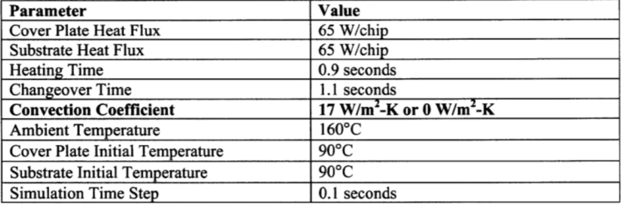
Table 4-4. Simulation parameters for convection coefficient study. Two simulations were run,
each with different convection coefficients...42
Table 4-5. Simulated surface temperatures after heating and changeover stages for varying
convection conditions...
42
Table 4-6. Simulation parameters for cover plate pre-heat study. Two simulations were run,
each with different Tinitiai...43
Table 4-7. Simulated surface temperatures after heating and changeover stages for varying
initial tem perature conditions...
44
Table 4-8. Process parameters for study of constant temperature boundary conditions applied
during changeover to back of cover plate and substrate. Two simulations were run, each
with a different Tboundary--- -.---...
44
Table 4-9. Simulated surface temperatures after heating and changeover stages for varying
constant temperature boundary conditions...45
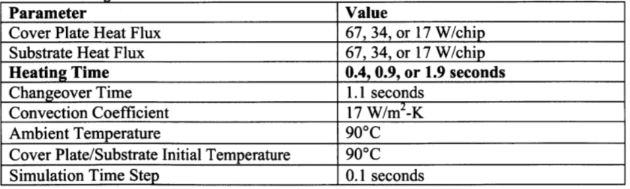
Table 4-10. Process parameters for heating time/heat flux study. Two simulations were run,
each with a different heating time...
45
Table 4-11. Simulated surface temperatures after heating and changeover stages for varying
heating tim e/heat flux combinations...
46
Table 4-12. Temperature gradients at surface of part after heating and changeover stages for
varying heating time/heat flux combinations...
46
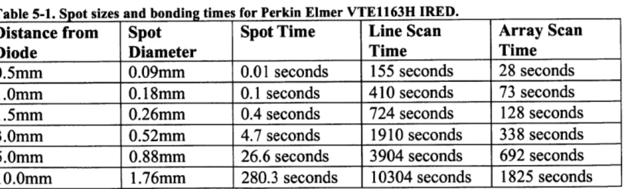
Table 5-1. Spot sizes and bonding times for Perkin Elmer VTE1 163H IRED...62
Table 5-2. Spot sizes and bonding times for OSRAM Ostar Observation IR Emitter (SFH
4740)...
. 63
Table 5-3. Power absorbed by different selective coatings from 50W and 100W light sources.
Light sources have a color temperature of 3000K. Assumes perfect absorption...76
Table 6-1. Commercially available integrating spheres from LabSphere...98
Table 6-2. Comparison of two integrating spheres on basis of light uniformity and power
requirem ents...
. 98
Table 6-3. Average post-bonding channel heights after bonding for different amounts of time
under various bonding conditions. Bonding was stopped after at least a few channels
were bonded. These were the channels that were measured and averaged. Cover plates
of various sizes were used. All parts were from the same embossing run except the
starred part, which was from a previous pFac run. Bold numbers indicate acceptable
post-bonding channel heights...140
CHAPTER
'
Research Motivation
1.1 Importance of Microfluidics
The field of microfluidics has taken off in the past couple of decades as a promising way
to create "labs on a chip." Microfluidic devices require a very small amount of liquid and can
be used to conduct powerful analyses in many arenas, including healthcare diagnostics, DNA
analysis, drug discovery and fuel cell technologies.
In 1990, Manz et al [1] discussed the miniaturization of a total chemical analysis system
to monitor the concentration of a chemical species. This was one of the first microfluidic
demonstrations, published even before the term "microfluidic" was coined. This research
showed that miniaturizing the total chemical analysis system would enhance its analytical
performance. Transport of fluid through the total chemical analysis system is faster when it is
miniaturized and less liquid is needed. As a result, chromatographic and electrophoretic
separations can occur more quickly and multiple processes could even run in parallel on one
chip.
A few years later in 1993, Gravesen et al [2] discussed the advances in the fluid
mechanics modeling that described the phenomena behind the microfluidic technology, and also
described the advances in micromechanical valves and micropumps to control fluid flow. These
elements are at the base design of most microfluidic devices. At the time, the most common
devices were flow sensors and there were a few simple microfluidic systems, such as inkjet
printer heads, on the market.
Since its infant stages, the field of microfludics has grown to include a variety of
microfluidic elements and applications. Daktari Diagnostics has developed a low-cost blood
analyzer to measure glucose levels [3], Caliper Life Sciences developed a chip for
electrophoretic DNA separation [4], and Choban et al developed a microfluidic based fuel cell
that could lead to the development of efficient room temperature based power sources
[5].
These are just a few of the many examples of microfluidic applications under investigation
today.
As Whitesides states, "As a technology, microfluidics seems almost too good to be true:
it offers so many advantages and so few disadvantages (at least in its major applications in
analysis)" [6]. However, microfluidic chips are not yet widely used, for there are still many
questions to be answered before it will become a major new technology, making it an intriguing
avenue for academic research.
1.2 Manufacturing Microfluidic Devices
As is described by Becker
[7],
the basic process to develop a microfluidic chip consists
of:
1. General design work
2. Microstructuring the substrate. This can include processes such as hot
embossing, injection molding, and laser ablation, among others. At the end of
this process, there exists a substrate with the desired microchannels in it.
3. Backend processes. Microstructuring generates the desired micro features, but
does not produce functional chips. About 80% of the manufacturing costs for
microfluidic devices stem from processes such as depositing electrodes, cutting
the device out of a larger master, and encapsulating the channels so that fluids
can flow through them.
The specifics of carrying out each of the above steps are dependent on the device's
material. Microfluidic devices have been made out of a variety of materials, including silicon,
glass, thermoplastic polymers and thermoset polymers. In general, polymeric materials have
lower costs associated with them, in terms of both material costs and manufacturing costs. In
applications such as low-cost healthcare diagnostics, it is also desirable to have disposable
devices, which is much easier with polymeric materials. Thermoset polymers are often used in
the lab environments because they can be cast and cured in small quantities. However, on a
larger scale, thermoplastic polymers are more desirable, both for their material properties and
their manufacturability. These thermoplastics include polymethylmethacrylate (PMMA), cyclic
olefin (co)polymer (COC), polycarbonate (PC), polystyrene (PS), and others.
The MIT Center for Polymer Microfabrication has been running a MicroFactory project,
pFac, in which the automation of manufacturing thermoplastic microfluidic devices is under
investigation [8]. In this project, the microfluidic mixer shown in Figure 1-1 below is
manufactured out of polymethylmethacrylate (PMMA).
Figure 1-1. Microfluidic mixer pattern used in the pFac project.
In this project, hot microembossing is used to complete the microstructuring step. The
blank substrate is heated to some temperature above the plastic's glass transition temperature.
At these elevated temperatures, the polymer begins to soften. A tool with a mold of the desired
channels is then brought in contact with the top surface of the substrate and pressure is applied
for a specified amount of time. After the softened polymer plastically deforms into the mold, it
is cooled and pulled off of the tool. The embossed substrate is now complete. Within the MIT
lab, Dirckx [9] and Hale [10] have worked on the development of equipment for the hot
microembossing process that achieves fast cycle time at low capital cost.
After embossing, the substrate moves to an inspection stage and then onto the bonding
stage. The bonding equipment used in this example was developed based on Hale's hot
embossing technology. The substrate and cover plate are both heated and then pressure is
applied to get the surfaces of the substrate and cover plate to bond together. This is a technique
commonly used in industry known as thermal bonding. Its details will be discussed further in
the next two chapters. Once bonded, the device can be functionally tested, to ensure that fluid
moves through the channels and mixes together as is intended.
One of the biggest challenges in the microfactory project, and in many microfluidic manufacturing environments, is the reliable and high-yield bonding of the microfluidic devices. As described by Ng et al., a good bond is high in strength, is leak-proof under high fluidic pressure, has a homogenous bonding interface free of voids, and has minimal deformation of microstructures [11]. It is also beneficial for the device to have high optical clarity, so that a user can view the fluid flowing through the channels.
An example of a bonded device that was not leak-proof is shown below in Figure 1-2.
Figure 1-2. Leaks on a microfluidic device due to insufficient bonding. Courtesy of Ali Beyzavi, NTU.
An example of a bonded microfluidic device with blocked channels due to excessive deformation during bonding is shown below in Figure 1-3.
Figure 1-3. Blocked channels on a bonded microfluidic device due to excessive deformation during bonding. Courtesy of Ali, Beyzavi, NTU.
There are many methods of bonding microfluidic devices, including adhesive printing, lamination film bonding, thermal bonding, surface modification, solvent bonding, and localized welding, each of which will be discussed in the next chapter. The optimal bonding method is different for every application. In many cases too, there is a method that works for one
microfluidic pattern, but adapting that method to other patterns takes a lot of adjusting and often results in a lot of wasted parts. Especially as microfluidics move further towards
commercialization, there is a great need for a high-yield, high-throughput method that is more robust to process changes.
This need has been definitively stated in the literature. In his 2006 article in Nature [6], Whitesides states, "An important aspect of the commercial development of microfluidics -crucial to many of these applications - is the development of the technology for manufacturing microfluidic devices." He then raises questions about many microfluidic manufacturing issues and ends with, "And what about technologies for sealing and packaging?" Even more recently, Tsao and DeVoe state in their 2009 review of microfluidic bonding technologies, "It is clear that the thermoplastic bonding technique need [to be] further advanced to superior compatibility to meet various microfluidic applications.. .the need for bonding methods which are compatible
with high throughput manufacturing will increase." It is this clear need for further developments in bonding technologies that motivated this research.
In this thesis, an innovative method of bonding is developed. This method uses light to provide both the bonding energy and the illumination for an in-process vision system for real-time viewing and control of the bonding process. This research sets the groundwork for a concept that, with further development, will be able to control the bonding of each chip individually, ultimately making the process more robust and high-yield.
CHAPTER
2
Current Microfluidic Bonding Methods
2.1 Bonding Thermoplastics
In 2009, Tsao and DeVoe [12] wrote a comprehensive review article of the various methods in existence to bond thermoplastic microfluidic devices. The methods reviewed included adhesive bonding, lamination film bonding, thermal bonding, surface modification, solvent assisted bonding, and localized welding. This chapter will review each of these methods, and will also consider the laser welding of microfluidic devices.
2.2 Adhesive Bonding
In adhesive bonding, glues are used to secure the substrate and cover plate. These glues include liquid adhesives that set when the solvent evaporates, epoxies and acrylics that cure after being mixed with a catalyzing agent, and thin layer high viscosity resins that are UV curable. The latter is the most common. One disadvantage of adhesive bonding is that the channel walls are no longer homogenous, as this resin forms part of the wall and could have an effect on the fluids flowing through the channels, particularly when the fluids are biologicial reagents. The biggest challenge with adhesive bonding is that the channels can get easily clogged with the glue being used. Careful application of the glue is critical.
An interstitial bonding technique has been developed that allows for the careful
placement of the glue only on the regions in between channels [13]. A diagram of this method is shown below in Figure 2-1. In this process, both the chip and cover plate are cleaned and dried. Resin is loaded in the loading reservoir and in a matter of seconds, capillary action draws
the resin into the appropriate interstitial space. The resin is precured for one minute to make it tacky and then postcured for two hours.
Resin loading reservoir
Cover plate 4- Interstitial space
Microchannel
UV-curable resin
4H14P
VNlight
Figure 2-1. Schematic of interstitial bonding technique [131
This process had almost 100% yield and was able to successfully bond PMMA to PMMA, glass, and PC. The thickness of the resin was small compared to the channel height, so there was negligible altering of the surface properties, though the channel wall was still not
100% homogenous. The resulting bond strengths were as follows: PMMA-PMMA: 9.3kPa, PMMA-glass: 12.4kPa, Scotch tape: 3. lkPa, thermal bonding at 110*C for 1 hour: 18.6kPa.
In another kind of adhesive bonding [14], PDMS was spin-coated in 10-25 pm thicknesses and then room temperature cured most of the way for 20 hours. The cover plate was then bonded to the microchip under pressure at 90*C for 3 hours. In this example, there was 100% bonding across the desired interface and a 15.7MPa bond strength.
Other types of adhesive application microcontact printing, screen-printing the adhesive onto a cover plate, and injecting the channels with a resin, applying a UV-curable adhesive, and then flushing the channels out with nitrogen before curing.
2.3 Lamination Film Bonding
In lamination film bonding, a thin polymer film is used as the cover plate and is laminated onto the substrate surface. In one example of lamination film bonding [15], thermal lamination was accomplished with a polyethylene terephthalate (PET)/polyethylene film in a standard industrial lamination apparatus. Lamination occurred at 125*C with less than 3 seconds of exposure to hot temperatures. The reservoirs that were needed to access the channels were laser ablated after lamination. The technique worked well and because of the low temperatures and rapid sealing times, it was also possible to predeposit sensitive biological reagents. The bonding was strong enough such that 40 tL/min could be externally pumped through the device. No leaks were detected and the profile above the channel showed no deformation of the lamination into the gap, even at 190 Rm wide.
In another example [16], the PMMA was annealed at 80*C for at least 90 minutes prior to bonding to avoid stress cracks in the structure. The PMMA structure was then heated at
100*C and a cold lamination foil was manually pressed onto the surface. The film only heated where it was touching the top surface of the substrate because of the low conductivity of air in the channels. The foil adhered to the substrate without the foil dissolving and clogging the channels.
In general, lamination film bonding is advantageous because there is minimal channel deformation and the process occurs quickly. However, the film can embed in the channel and since the film is a different material than the substrate, the channel walls are non-homogenous.
2.4 Thermal Bonding
In thermal bonding, the substrate and cover plate are heated to a temperature slightly greater than the glass transition temperature of one or both of these pieces. Pressure is then
applied to increase the contact forces between the two pieces. This combination of elevated temperature and pressure results in sufficient flow of the polymer at the interface and
interdiffusion of the polymer chains between the surfaces. With this method, it is feasible to create an optically clear homogenous bond, which is highly desirable in microfluidic
applications. However, this process can also be very low-yield because the optimal bonding parameters are different for every application. Even just slight changes to the grade of material or the microfluidic pattern itself can cause the need for an adjustment to the bonding
parameters. Channel deformation or voids in the bonded area can result if the process conditions are not optimized.
Nevertheless, the simplicity of this process and the reasonable bond strength that can be achieved makes it a promising option that is widely studied and implemented. The simplicity is clear in implementations such as that by Sun et al [17]. The PMMA pieces to be bonded were placed on a hot plate and an aluminum plate was placed on top of them. Weights on top of the aluminum plate provided the pressure and the heating was controlled by adjusting the hot plate temperature. This particular study used high hot plate temperatures, on the order of 165*C, low pressures, typically 20kPa or less, and long time frames, on the order of 30 minutes.
In another implementation of thermal bonding, Chen et al [18] was successful at bonding two PMMA pieces at 1 10*C for 20 minutes. Zhu et al [19] studied bonding temperatures between 88*C and 100*C and pressures between IMPa and 3MPa for bonding PMMA. Huang et al [20] bonded PMMA to PMMA using pressures of 1.25 kPa for 3 minutes, after heating for 12 minutes (heating temperature unreported).
In just these few examples of thermal bonding, the range of temperatures and pressures is vast, as is the complexity of the bonding equipment. There was successful bonding in each of
these examples, though, which is why the technique is common. It is just a matter of choosing the right parame'ters.
2.5
Surface Modification
By modifying the substrate and cover plate surfaces to be bonded, there is an increase in the surface energies, which improves the wettability of the substrate and cover plate, allowing better contact and increasing the interlocking of the polymer chains across the interface. The surface modifications also generate electrostatic interactions and can produce hydrogen or covalent bonds across the interface if the modification is in the form of polar functional groups.
In an example of monomer modification [19], the PMMA was modified with its monomer, methylmethacrylate, before being thermally bonded. This modification decreased the glass transition temperature of the surface, thus allowing the surface of the part to soften more than the bulk when the temperature was raised. The thermal bonding occurred at 95*C and 2MPa for 3 minutes. In this particular study, the bond strength was monitored over time and compared to two pieces that were thermally bonded without surface modification. It was found that the bond strength over time was higher and steadier when the surface was modified prior to thermally bonding it. The maximum bond strength achieved without channel collapse was IMPa.
It is also possible to modify the surface with ultraviolet light. In one example [21], the surfaces of PC were exposed to UV radiation for 30 minutes. The radiation had a wavelength of 254nm and a UV intensity of 15 mW/cm2. This surface modification also lowers the glass transition temperature of the surface. Bonding temperatures were varied between 146*C and 160*C and the bonding time was fixed at 30 minutes. A bonding temperature of 150*C was
chosen in the end because it resulted in sufficient sealing without deforming the microstructures. Fluid was sent through the device and no leaks were detected.
Treating the surfaces with UV/ozone produces energetic surfaces and results in at least 1-2 orders of magnitude improvement in bond strength for PMMA and COC, and allows the bonding to occur at temperatures well below the glass transition temperature with a good degree
of control over the hydrophilicity of the surfaces [22]. In this example, the surfaces were exposed to the UV/ozone with a commercial ozone cleaning system. They were then rinsed with IPA and DI water and dehydrated in a vacuum oven for two hours. They were finally inserted into a hot press at 4.8MPa for 10 minutes. Both PMMA and COC were successfully bonded in this way.
Plasma treating the thermoplastic oxidizes the surfaces being bonded. This removes the dust and polishes the part, shortens the polymer chains at the surface, and lowers the surface layer's melting temperature to be much lower than the temperature of the bulk polymer [16].
While surface modifications have been shown to have a positive effect on the bonding quality of microfluidic devices, the presence of a surface modification is not always ideal. Surface modifications alter the surface chemistry of the interfacial surface and often the channel walls as well. The surface chemistry can have an effect on the fluid flow through the channels, especially in biological applications, and so altering these surfaces is not always an option.
2.6 Solvent Assisted Bonding
Similar to bonding with surface modifications, solvents can also be used to facilitate better bonding. When a thermoplastic surface is solvated, the polymer chains become mobile and can diffuse across the interface better, resulting in high bond strength. At the same time, the softening of the polymer surface may cause even more channel collapse than would have
occurred otherwise. Solvent bonding is very similar to surface modification bonding in that the solvent facilitates better bonding, but alters the surface chemistry of the polymer.
A variety of solvents have been used for this purpose, including methylcyclohexane [23], acetronile [24], and ethanol [16]. In some examples, the solvent bonding is also
accompanied by the use of phase-changing sacrificial materials in the microfluidic channels. In one case [25], paraffin wax filled the PMMA channels and acetronile was used for solvent assisted bonding. The hardened wax in the channels prevented the softened PMMA from collapsing during the bonding process. Once the bonding was complete, the wax was melted out of the channels.
2.7
Localized Welding
In localized welding, a thin layer of the surface of the cover plate and substrate is melted for enough time that the two melted surfaces at the interface will weld together. The process happens quickly enough that the high temperatures only affect the surface layers of the plastic, and the bulk remains rigid and doesn't deform.
In ultrasonic welding, area contact energy directors are built into the design of the microfluidic part in between channels. The substrate and cover plate are then clamped together and ultrasonic vibration is applied. In one example [26], ultrasonic vibration with an amplitude of 13 tm, a bonding pressure of 0.32MPa, and a bonding time of 8s, was applied and the resulting part was able to sustain a burst pressure of 680-800 kPa and had a bonding strength of 2.25MPa.
In microwave bonding, gold or another metal film is deposited on the surface of the PMMA and the substrate and cover plate are clamped together. The stack is then exposed to
microwaves, selectively melting the film and causing localized melting of the PMMA. In one trial of this technique [27], a bonding strength of 0.7MPa was achieved.
In both of the above examples, the localized welding achieves a good bond, but the implementation of energy directors or the addition of metal films adds complications to the process. In particular, adding metal films can cause problems when electrodes or other metallization is required to make the microfluidic device function.
2.8 Laser Welding of Plastics
Similar to the localized welding of microfluidic devices, laser welding involves
generating a weld seam across the interface through the use of laser energy. In many cases, in order to accomplish localized welding at the surface, the laser travels through a transparent cover plate and gets absorbed by an opaque substrate. While the weld seams generated by this method are good, the device by nature will no longer be optically clear because of the opaque substrate. Malek [28] explains in his review of laser bonding techniques, that the opaque-transparent laser bonding is well-established but there is still much room for innovation in transparent-transparent laser bonding. Existing methods of laser bonding that were discussed include using carbon black coatings as a selective absorber [29, 30], using a hybrid laser-IR welding technique, and using reverse conduction welding with an IR-absorbing backplate that absorbs and retransmits the heat through a thin-film cover plate [31]. Only the latter of these methods would result in an optically clear weld.
Also discussed though, were examples of microfluidic bonding using ClearweldC, an infrared absorbing dye made by Gentex, that was developed for welding optically transparent polymers [32]. This dye absorbs certain wavelengths of NIR and IR radiation and is highly transparent in the visible. The dye can either be incorporated into the bulk, which leads to slight
discoloration, or can be applied as a thin film. This again would require the addition of a foreign material into the bonding area, which might not always be ideal. Lai [33] was able to
successfully bond a three-layer microfluidic chip using Clearweld at the interface and a fiber-coupled 808nm diode laser. The laser beam moved around the channels to create a weld seam in the appropriate locations; this relative motion was accomplished with moving stages. In a tensile test, the parts bonded in this way achieved a bonding strength of 58MPa.
2.9 Research Direction
Each of the above methods that have been reviewed has its distinct advantages and disadvantages, and clear areas for possible innovation. One of the main goals of this research was to investigate a method that could be adapted to high-throughput manufacturing processes, such as the MIT [tFac project. Of all of the methods mentioned, the thermal bonding method was the simplest in terms of process complexity and had the most examples of scale-up for manufacturing. Furthermore, other than ultrasonic welding, it was the only method that also generated an optically clear homogenous bond. For these reasons, thermal bonding and localized welding were at the forefront of thinking in choosing a research direction.
The next chapter will look at the mechanisms behind thermal bonding in more detail and will also investigate the idea of localized welding/interface heating.
CHAPTER
3
Thermal Bonding and Interface Heating
3.1 The Thermal Bonding Process
As was described in chapter 2, during the thermal bonding process, the substrate and
cover plate are heated to a temperature greater than the glass transition temperature and pressure
is applied to facilitate bonding across the substrate-cover plate interface. A schematic of this
process is shown in Figure 3-1 below.
Cover Plate
Substrate
Pressure
Figure 3-1. Schematic of a conventional thermal bonding setup. The substrate and cover plate are clamped in between two heaters. Both pieces are brought up to a temperature greater than their glass transition
temperature and pressure is applied to facilitate bonding across the interface.
The physics of what is happening at a molecular level during the bonding process is
rooted in the reptation model of diffusion. When the material heats up, the polymer chains
begin to flow. It is the intertwining of these chains across the interface that causes the bonding
to occur. In the reptation model [34], shown in Figure 3-2 below, the molecules are described
as sliding, or "reptating," through a "tube." The tube contours are defined by the locus of
entanglements with neighboring molecules, with the motion of the polymer chains transverse to
the contour of the tube severely restricted.
Polymer chain
Other chains in the system --- Primitive chain
Figure 3-2. Reptation model of interdiffusion. The molecules are described as sliding, or "reptating," through a "tube." The tube contours are defined by the locus of entanglements with neighboring molecules,
with the motion of the polymer chains transverse to the contour of the tube severely restricted. [341
The diffusion process is measured by the diffusion coefficient of the polymer, which is
dependent on the temperature and viscosity of the material. The stages of diffusion can be
described as is shown in Table 3-1 below.
Table 3-1. Stages of polymeric diffusion according to the reptation model [341.
Stage
Time Stage
What's Happening
Average
Starts
Displacement of
Chain Segments
Chains do not feel constraints of
-t 1/4surrounding chains
2 tentangle Perpendicular movement restricted ~t_1/ _
3
Movement of segments of whole chain
14tRouse becomes correlated
4 treptation Fickian diffusion dominates ~t 1/2
The polymer's radius of gyration, self-diffusion coefficient, and molecular weight define
the
tentangle, tRouse,and
treptationtime constants. Kunz and Stamm
[35]
used neutron reflectometry
to study the interface of protonated and deuterated PMMA films and estimated these constants
to be 13min, 48min, and 1547min, respectively. The interface widths at these times were shown to be 3.9nm, 3.9-4.7nm, and 5.8-7.2nm respectively.
These times scales are very long compared to the desired time scales for a high-throughput scenario. The [tFac project targets a takt time of 5 minutes. With embossing processes taking on the order of minutes, a 2-hour long bonding process is not ideal. Elevating the temperatures of the polymer can decrease these time constants, which is a promising case for high-temperature thermal bonding. Furthermore, the polymers are placed under pressure for two reasons during the thermal bonding process. The first is to ensure that there is contact between the substrate and cover plate surfaces. The second is to facilitate the flow of the polymeric chains. As such, the combination of elevated temperatures and pressures can allow
for faster bonding.
In a conventional thermal bonding setup, the temperature of the entire cover plate and substrate must be brought up to the bonding temperature. Therefore, bonding at high
temperatures is not ideal because the entire substrate will soften, resulting in excessive channel deformation. However, in localized welding applications, heat is only applied at the interface, allowing the rest of the substrate to maintain its rigidity during the welding process. Focusing on this concept of interfacial heating can be powerful in a number of ways, which will be described in the next section.
3.2 Interfacial Heating
Interfacial heating can be beneficial in both welding and thermal bonding applications. In welding, a thin layer at the interface is quickly melted and low pressures are applied to weld the surfaces together. The welding process occurs in three phases, shown in Figure 3-3 below [36]. In the first two stages, the interface has no mechanical properties and two distinct
faces still exist. In the last phase, wetting occurs, as intimate contact between the two surfaces
has been achieved and potential barriers associated with inhomogeneities at the interface
disappear. The molecular chains are now free to move across the interface in reptation. Once
the reptation time has elapsed, the chain forgets its original configuration.
a)
b)
)Figure 3-3. Phases of welding. a) and b) The interface has no mechanical properties and two distinct faces still exist. c) Wetting - intimate contact between the two surfaces has been achieved and potential barriers
associated with inhomogeneities at the interface disappear. The molecular chains are free to move across the interface in reptation. Once the reptation time has elapsed, the chain has forgotten its original
configuration. [361
In interfacial heating for thermal bonding, the interfacial surfaces would be heated to a
temperature greater than the glass transition temperature of the polymer. However, instead of
the entire part being heated to this temperature, a temperature gradient would form throughout
the thickness of the substrate and cover plate. As a result, the surface layer of the substrate
would be the softest. When pressure is applied, this surface would experience the most
deformation, with less deformation occurring throughout the thickness of the channels. The
deformation that occurs is a result of both polymeric diffusion and basic compression of the
plastic. There is an operating region right around the glass transition temperature in which the
modulus of elasticity of a thermoplastic is highly dependent on the temperature. This
Young's modulus of a material is proportional to the shear modulus, its general trends are still useful to look at.
PA
Oj80
0
C
Figure 3-4. Model for temperature dependence of shear modulus. The glass transition temperature of 80*C is specified here for PETG. Model can be used for other Tg's as well. The AO gap is typically 30*C. [371
As this model shows, in a region around Tg, the modulus is highly dependent on
temperature. If the immediate surface were to be bonded at a temperature above Tg but within
the AO gap, then there would be a temperature gradient throughout the substrate, and also a modulus gradient throughout the substrate, with the modulus at the layers beneath the surface being higher than the modulus of the surface itself. As such, the substrate would be stiffer than the surface, resulting in less deformation of channels and more deformation right at the surface
where the bonding occurs. At temperatures beyond this AO gap, there is still a small
dependence of modulus on temperature, implying that this reasoning would be valid at high
temperatures as well, depending on how steep the temperature gradients were. With this reverse
temperature gradient, it might be possible to apply higher pressures with less total channel
deformation in a pure thermal bonding application.
3.3 Research Focus
Based on the literature review and preliminary thinking on the topic, interfacial heating was chosen as the main bonding technology to focus on. A variety of methods were explored,
each of which will be presented in the next chapters. For the analysis and thinking done here, the RFac microfluidic mixer from Figure 1-1 was considered. This part is currently made out of
PMMA. The thermal properties of the PMMA vary depending on the commercial grade of the material. For the analyses done here, the following thermal properties were assumed: Tg=90 C,
CHAPTER
4
Three-Stage Non-Contact Surface Heating
4.1 General Concept
The basic concept of three-stage, non-contact surface heating is depicted below in Figure 4-1. In the first step, the cover plate and substrate are held apart a small distance from one another and a heater heats the surfaces of each. In step 2, the heater is removed, and in step 3, pressure is applied to the cover plate-substrate stack in order to promote interfacial diffusion.
1:
2:
3:
Heater
Figure 4-1. The basic concept of three-stage, non-contact surface heating. In step 1, the cover plate and substrate are held apart a small distance from one another and a heater heats the surfaces of each. In step 2,
the heater is removed and in step 3, pressure is applied to the cover plate-substrate stack in order to promote interfacial diffusion.
This process is similar to hot tool welding and infrared welding described by
Yousefpour et al in their review of fusion bonding and welding of thermoplastic composites [38]. However, this review focused on the welding of large rods of material in which case the preservation of fine features, such as microfluidic channels, was not important. A
displacement-controlled hot plate welding system was described by Stokes [39]. In this system, the two pieces being welded were brought into contact with a hot tool and pressure was applied to ensure contact. The pressure was then lessened to allow the melt region to grow, the heater was removed, and the parts were brought together and held under pressure to allow the bond/weld to form. This system was used to bond thinner plates of plastic, on the order of a
![Figure 5-8. Absorbance profile of Fabricolor Dye 8472, peak absorption at 848nm. [51]](https://thumb-eu.123doks.com/thumbv2/123doknet/14733377.573544/59.918.172.736.223.645/figure-absorbance-profile-of-fabricolor-dye-peak-absorption.webp)