Design, Modeling, and Simulation of a Compact
Optoelectronic Neural Coprocessor
by
Travis L. Simpkins
Bachelor of Science in Electrical Engineering and Applied Physics Case Western Reserve University, 2000
Master of Science in Electrical Engineering and Computer Science Massachusetts Institute of Technology, 2002
Submitted to the Department of Electrical Engineering and Computer Science in partial fulfillment of the requirements for the degree of
Doctor of Philosophy in Electrical Engineering and Computer Science at the
MASSACHUSETTS INSTITUTE OF TECHNOLOGY October 2005
@
Massachusetts Institute of Technology 2005. All rights reserved.A u th or ... ...
Department of Electrital Engineering and Computer Science October 24, 2005
Certified by ... .
Cardinal Warde Professor of Electrical Engineering and Computer Science visor
Accepted by ... ....
Arthur U. Smith Professor of Electrical Engineering and Computer Science Chairman, Department Committee on Graduate Students
MASSACHUSETTS INSTITUTE OF TECHNOLOGY
JUL 1
0
2006
Design, Modeling, and Simulation of a Compact Optoelectronic Neural Coprocessor
by
Travis L. Simpkins
Submitted to the Department of Electrical Engineering and Computer Science on October 24, 2005, in partial fulfillment of the
requirements for the degree of
Doctor of Philosophy in Electrical Engineering and Computer Science
Abstract
Microprocessors have substantially increased in speed and computational power over the past two decades. However, they still are unable to solve certain classes of problems effi-ciently, particularly those which involve the analysis of large noisy data sets such as the case of image processing, feature extraction, and pattern recognition. Substantial research has focused on using neural network algorithms to process this type of data with much success. Most of this effort, however, has resulted in sophisticated neural network-based software algorithms rather than physical neural network hardware. Consequently, most neural network-type processing systems today consist of neural algorithms running on tra-ditional sequential (i.e. Intel-based) microprocessors rather than on actual neurocomputers, and thus achieve less than optimal performance.
The objective of the Compact Optoelectronic Neural Coprocessor (CONCOP) project is to build a compact, pixilated, parallel optoelectronic processor capable of running neural network-type algorithms in native hardware. While much of the past research on the project has focused on designing and implementing the microphotonics and optoelectronics required for interlayer communication within the system, the work presented in this thesis will begin
by focusing on the computational components, particularly the mixed-signal integrated
circuits located in each pixel. After the circuits have been designed, a progressive training and simulation environment will be developed based on hierarchal system models which provide accurate, timely, and efficient performance estimates of the CONCOP while it is still in the pre-integration stage. Using this simulation platform, several simulations of the
CONCOP will be performed to demonstrate the flexibility of the environment and to better
understand the scalability and fault-tolerance aspects of the CONCOP. The results of a test chip containing the fundamental circuit components will also be presented.
Thesis Supervisor: Cardinal Warde
Acknowledgments
I would first like to thank Prof. Cardinal Warde for his support of my research. Without
him, it obviously would not have been possible. I have benefited tremendously from his wisdom, experience, vision, and encouragement over the years, and I look forward to our continued collaboration.
My thesis committee has been very helpful in steering the direction of my research. As
co-principal investigator on the project, Prof. Clifton Fonstad has had many contributions. Prof. Duane Boning has continued to support my research since my early days at MIT, even as his departmental responsibilities have grown exponentially. I certainly appreciate their willingness to squeeze yet another meeting into their schedules.
Although my colleagues in the Photonic System Group may have been small in number, they have still had great influence on my work. Dr. Ben Ruedlinger has been a friend and mentor since our days together in Suite 820 at CWRU. Ben's prior work on the CONCOP accelerated my research, and for this I am quite appreciative. David Dunmeyer has been an incredible resource for all that is optical (and much that is not). It has been fun sharing a bit of culture (and an office) with Yasushi Takamatsu, our visiting scientist from Japan. Additionally, Gustavo Gil, Gille Hennefent, and Marta Ruiz-Llata have also been enjoyable to work with. Down the hall in Prof. Fonstad's group, I would thank James Perkins and
Ed Barkley for their contributions and collaborations along the way.
I've been fortunate to have made some great friends while at MIT. When David (and Sarah) Wentzloff and I first met at Intel in 1998, I do not think either of us ever imagined we'd eventually graduate from MIT together. Benton Calhoun has been a great friend over the years as has Harry Lee. I would also like to thank Frank Honore, Micah O'Halloran, Ed Filisko, Fred Lee, Mark Spaeth, John Fiorenza and countless others for making my years at MIT more enjoyable.
My work has also been helped by people outside of MIT. As always, I'm appreciative of
my friends from Suite 820 at CWRU - Kent Lee, Dan Baker, Dan Prorok, Aaron Carkin, Steve Troyer, and Ben Ruedlinger. Prof. Francis Merat and Prof. David Smith both provided guidance during my CWRU years, while Jim Duxbury, James Powell, Bill Yerman, Joyce Fast, and David Tibbitts were instrumental during my Orrville days. Additionally, Paul Maccoux and Jason Gayman at Intel, Stephen Clarke at Agilent, and Jeff Tracey at
IBM have given me an industry perspective at various points along the way.
The sponsors of my research have obviously played an important role. I was originally funded by the National Defense Science and Engineering Graduate (NDSEG) Fellowship and was later funded by the National Science Foundation (NSF). Without their belief in the future of optoelectronic neural hardware this project would not have been possible.
Finally, I would like to thank my parents, Jerry and Mary Ellen Simpkins. When they first put me on that bus to kindergarten in 1982, I'm sure they didn't expect it would take me over 22 years to finally get out of school! They are the standard by which all parents should be measured. Thanks Mom and Dad!
Contents
1 Introduction
1.1 Background on Neural Computing . . . .
1.1.1 Hopfield Networks . . . . 1.1.2 Multilayer Perceptrons (MLP) . . . .
1.2 Prior Hardware Implementations of Neural Networks Utilizing Optoelectronics 1.2.1 MLP using Bench Optics at UCSD . . . . 1.2.2 MLP for Robot Control at FSU . . . .
1.2.3 Digital Bus-Based Neural Networks . . . .
1.2.4 Discussion of the Selected Prior Neural Network Processors . . . . .
21 22 25 26 28 29 33 37 40
2 The CONCOP Project 43
2.1 Background of the CONCOP Project . . . . 44
2.2 Prior Work on the CONCOP . . . . 47
2.2.1 Holographic Interconnections . . . . 48
2.2.2 Optoelectronic Device Development and Integration . . . . 49
2.2.3 Architecture of the CONCOP . . . . 50
2.3 A New System Architecture for the CONCOP . . . . 55
2.3.1 Supporing Lateral Interconnects . . . . 57
2.4 Implementation of the Proposed CONCOP Architecture . . . . 58
3 Circuits for the CONCOP 61 3.1 Neuron Summing Circuits . . . . 62
3.1.1 Transimpedance Amplifier . . . . 62
3.1.2 Single-to-Differential Converter . . . . 66
3.2.1 3.2.2 3.2.3 3.2.4
Binary-Weighted Current Source . . . . Operation of the Differential Pair . . . . Variable Gain Control . . . . Differential-to-Single-Ended Conversion with Translational Adjustment
3.3 Auxiliary Circuits
3.3.1 3.3.2 3.3.3
Reference Voltage Generator . VCSEL Drivers . . . . Weight Storage . . . . 69 71 77 80 . . . . . 82 . . . . . 83 . . . . . 83 . . . . . 86
4 Modeling and Training the CONCOP 87 4.1 T raining . . . . 87
4.1.1 Backpropagation . . . . 88
4.1.2 Parallel Weight Perturbation . . . . 90
4.2 System M odels . . . . 94
4.2.1 Ideal Mathematical Model as Implemented by Matlab . . . . 95
4.2.2 Functional Model based on Characterized Circuit Components . . . 95
4.2.3 SPICE Transistor-level Model . . . . 100
4.2.4 Extending the Models to Include Lateral Connections . . . . 101
4.3 Progressive Training Methodology . . . . 102
5 Simulation and Performance Analysis of the CONCOP 105 5.1 Training a 2x2x1 Network to Perform Boolean Logic Functions . . . . 106
5.2 Training a 12x12x5 CONCOP to Perform Face Recognition . . . . 113
5.3 Training Simulations on a CONCOP with Lateral Connections . . . . 119
5.4 Additional CONCOP Simulations . . . . 121
5.4.1 Simulations of Increasingly Larger CONCOP Systems . . . . 121
5.4.2 Simulation of a 12x12x5 CONCOP under Non-Ideal Conditions . . . 122
6 Conclusion 129 6.1 Summary of Contributions. . . . . 129
6.2 Discussion of Future Work. . . . . 130
6.2.1 Scalability . . . . 131
6.2.2 A pplications . . . . 132
6.2.3 Architectural Enhancements: Elman Network Variations . . . . 133
6.2.4 C ircuit D esign . . . . 134
6.2.5 Training, Modeling, and Simulation . . . . 134
6.2.6 Integration . . . . 135
A The Test Chip and Results 137 A.1 Testing Methodology . . . . 137
A.2 Neuron Circuits . . . . 138
A.3 Synapse Circuits . . . . 139
A.4 Auxiliary Circuits . . . . 141
A .4.1 Shift R egister . . . . 141
A.4.2 VCSEL Landing Site Integration . . . . 142
A.4.3 VCSEL Driver . . . . 142
A.5 Schematics, Diagrams, and Photographs . . . . 143
B Matlab Code for Simulating a 2-Input Boolean Logic Network 149
List of Figures
1-1 Model of a basic neuron with four synapses . . . . . 23
1-2 Common neuron transfer characteristics: sigmoid (dotted), hard-limit (solid), and linear (dashed). Again, much of the inspiration comes from neural science where neural transfer functions have been measured and modeled [3, 4, 5, 6, 7]. 25 1-3 A Hopfield network with four neurons (N0-N3), four inputs (XO-X3), and four outputs (Y0-Y3). . . . . 26
1-4 Multilayer perceptron with one input, one hidden, and one output layer. . . 27
1-5 Multilayer perceptron with Elman-style memory elements. The memory ele-ments store the previous output of the neuron and feed this value back during the next
cycle.
. . . . 281-6 Planar schematic of the UCSD MLP [22]. . . . . 30
1-7 Sample image at various stages of the UCSD MLP [22]. . . . . 30
1-8 Circuit schematic of the UCSD MLP with four synapses and one fan-in unit [2 2 ]. . . . . 3 1 1-9 Block diagram of the USCD MLP neuron [22]. . . . . 32
1-10 The FSU MLP with 1 input, 2 hidden, and 1 output layer [23]. . . . . 33
1-11 Digital processing block of the FSU MLP [23]. . . . . 35
1-12 Transmitter and receiver configuration in the FSU MLP [23]. . . . . 35
1-13 Hitachi bus-based architecture with four neurons. [27]. . . . . 38
1-14 Neuron structure of the Hitachi bus-based architecture. [27]. . . . . 38
2-1 The CONCOP being used for image enhancement and clutter removal. Adapted from [29]. . . . . 44
2-2 The CONCOP unit pixel. The unit pixel is tiled and cascaded in a 3-D array to create the CONCOP. . . . . 45
2-3 Floorplan of a single pixel of the CONCOP. (features are not to scale) . . . 46 2-4 The longitudinal nearest-neighbor interconnection system. A pixel in one
plane communicates with nine pixels in the succeeding plane through the use of nine VCSELs and a Bragg holographic interconnection array for beam steering [29]. . . . . 48
2-5 Profile view of a single pixel of the CONCOP showing VCSELs integrated onto a silicon wafer alongside CMOS circuitry. The substrate has been thinned to increase sensitivity to the optical inputs [31]. . . . . 50 2-6 Previous system architecture of the CONCOP with both optoelectronic and
electronic neurons. Each electronic neuron receives inputs from 5 co-planar optoelectronic neurons and transmits its output to 9 optoelectronic neurons in the succeeding plane. The figure shows three planes of neurons, each of which contains two logical layers of neurons. Adapted from [32]. . . . . 51 2-7 Training times for four interconnect schemes between co-planar layers. . . . 53 2-8 New CONCOP architecture with all optoelectronic neurons. Each neuron
receives inputs from nine neurons in the previous plane and transmits its output to nine neurons in the succeeding plane. All neurons implement
a sigmoidal transfer function which increases computational power and all interlayer communications are done optically. Each of the three layers of optoelectronic neurons shown in the figure requires its own plane. . . . . 56 2-9 An extension of the proposed CONCOP architecture to support lateral
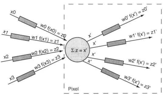
con-nections. In addition to the inputs from the previous plane, each neuron receives inputs from the eight surrounding neurons on the same plane. . . 58 2-10 The inputs and outputs of a single neuron represented by the central circle.
Each rectangle represents a synapse, such that a neuron and the succeeding synapses comprise one pixel of the CONCOP. The preceding synapses are associated with pixels in the preceding layer. . . . . 59
2-11 Block diagram of one pixel of the CONCOP. . . . . 60
3-1 Transimpedance amplifier based on an operational amplifier with a large feedback resistor. . . . . 62 3-2 Transimpedance amplifier based on an inverter with a biasing transistor. . . 63
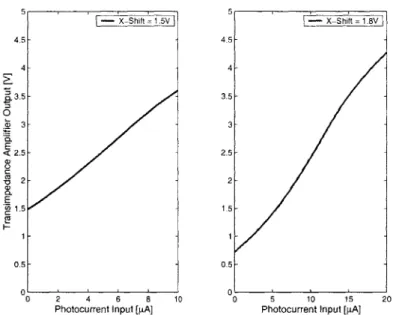
3-3 Transimpedance amplifier output for the expected operating range of 0-10 pA with Vx-shift = 1.5 V and for an extended range of 0-20 pA with Vx-shift =
1 .8 V . . . . . 6 5
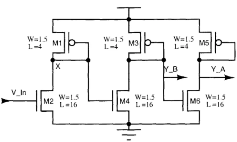
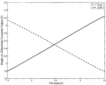
3-4 Test chip results confirming the operation of the transimpedance amplifier. The voltage output of the amplifier is plotted vs. the current input. .... 65 3-5 Single-ended to differential converter circuit . . . . 66 3-6 Results from the test chip illustrating the linearity of the differential outputs
for the single-to-differential converter. . . . . 67 3-7 A differential pair is at the core of the synapse and it is surrounded by four
key blocks. . . . . 68 3-8 The binary-weighted DAC current source with the transistor-level
represen-tation on the left and switch-level depiction on the right. Signals bO - b4 are
the individual bits of the locally-stored weight, and VrO - Vr4 are reference voltages distributed globally. . . . . 69 3-9 Basic differential pair which comprises the core of the synapse. . . . . 71 3-10 Synapse differential output current vs. differential input voltage for weights
±1, ±2, ±4, ±8, ±16, and ±31. . . . . 77 3-11 Level-shifting variable gain control circuit. . . . . 78 3-12 Test chip results demonstrating the variable gain control for a weight of
+31.
The inputs to the synapse were swept across the operating range for various VGain settings . . . . . .. . . . . .. 79 3-13 The difference circuit for the synapse. The output is the difference of Iin+
and Ii,_. VShift-UP and VShift-DN provide translational adjustment in the y-d irection . . . . . 80
3-14 Full schematic of the synapse. . . . . 81 3-15 Synapse output current vs. differential input voltage for various weights ±1,
±2, ±4, ±8, ±16, and ±31. . . . . 82 3-16 Test chip results showing the characteristic sigmoidal transfer function of the
synapse for weights ±1, ±2,±4, ±8, ±16, and ±31. . . . . 83 3-17 Reference voltage generator circuit for binary weighted synapses. . . . . 84
3-18 VCSEL driver with integrated transimpedance amplifier and current sink
3-19 VCSEL driver circuit transfer characteristic. The modulator transistor VDS = 2 V to simulate the operating characteristic of the VCSEL. . . . . 85 3-20 D-Flip-Flop chain for storing a 6-bit weight. . . . . 86
4-1 Backpropagation flow chart. Training proceeds until error E is reduced below some arbitrary level Emax. . . . . 89
4-2 Weight perturbation algorithm flow chart. The weights are updated based on the error difference between the upper and lower loops. Training proceeds until MMSE performance metric is met. . . . . 91
4-3 Modified weight perturbation algorithm flow chart. The lower loop repeats until a better set of weights are found. Whereas the standard WP algorithm adjusts the weights based on the error difference between the upper and lower loops, the modified WP algorithm simply keeps the weights which improve the overall error. ... ... 93
4-4 Graphical representation of the Modified Mean Squared Error (MMSE) per-formance metric. Outputs in the central (red) bands are not acceptable, outputs in the middle (yellow) bands are acceptable but will continue to be penalized in the hopes of reaching the target, while outputs in the outer (green) bands have exceeded the target and are considered to have zero error. 94 4-5 Verification of the functional synapse model. The solid curves represent the
functional model approximation of the current generated by each bit of the synapse, while the dashed curves represent the actual transfer characteristic as given by SPICE . . . . 98
4-6 Verification of the functional neuron model. The solid curves represent the functional model approximation of the voltage output of the transimpedance amplifier, while the dashed curves represent the actual transfer characteristic as given by SPIC E . . . . 99
4-7 Schematic of a 4x4x3 electronic CONCOP generated automatically using Cadence SKIL code. The SKIL code automatically connects the neurons according to the interconnection scheme specified. . . . . 100
5-1 The XOR truth table on the left with a graphical representation of the XOR outputs (X's and O's) as a function of inputs (X14x2) on the right. It is
impossible to draw one line which sorts the outputs into two categories and therefore the function is non-linearly separable. . . . 107
5-2 Block diagram of a (2,2,1) neural network to solve 2-input Boolean logic
functions such as XOR. . . . . 107 5-3 Physical implementation of the 2-input Boolean logic network. . . . . 108
5-4 Synapse weights which allow the 2-input Boolean logic network to function as an X O R gate. . . . . 110 5-5 Progression of the nine weights from an initial random state as the 2-input
Boolean logic network is trained to perform the XOR function. . . . . 110 5-6 Modified mean squared error of the output as the training progresses. It is
not a monotonically decreasing function. . . . .111
5-7 Graphical representation of the outputs of the 2-input Boolean logic network
after training. . . . . 112
5-8 Histogram of 100 training iterations for the 2-input Boolean logic network
trained to perform the XOR function. Count is the number of iterations in a given bin . . . 112
5-9 The training set consisting of three test subject images. Each image is a
12x12 8-bit grayscale array. . . . 113
5-10 The 12x12x5 network for face recognition. Patters are applied on the left
and outputs emerge from the right. Each of the five layers contains 144 pixels. 114
5-11 The 12x12x5 CONCOP was trained to recognize the three test subjects.
After training had completed, the system was verified by presenting each of the three test test subjects and observing the output. The dashed lines indicate the minimum acceptable output levels. . . . 115
5-12 The test set consisting of three test subject images where each individual has
donned a pair of glasses to slightly alter their facial characteristics. . . . . . 115 5-13 Graphical results from the test set. After each subject's appearance was
5-14 Average training time for a 12x12xN CONCOP where N varied from 4 to
8 for the original test subject image patterns. Each system was trained 10
tim es to obtain the average. . . . . 117
5-15 The expanded training set consisting of nine test subjects. Each image is a
12x12 pixel, 8-bit grayscale image. . . . . 118
5-16 Graphical representation of the results from exploring the capacity of the
12x12x5 CONCOP. Note that each of the nine outputs exceeds the minimum showing successful learning of the training set. . . . . 118
5-17 A 12x12x5 CONCOP with three dead pixels simulated to demonstrate fault
tolerance. Pixel (6,6) has been removed from layers two, three, and four of the system. The system is still able to function properly without retraining. 123
5-18 A 12x12x5 with eighteen dead pixels. The 3x3 square of pixels between (5,5)
and (7,7) have been removed from layers two and three. Despite the severe fault, the system still correctly identifies the three test subjects, albeit with very low noise m argins. . . . . 123
5-19 Graphical representation of the results from the fault tolerance simulations.
On the left, the ideal CONCOP identifies the subjects and meets the noise margin thresholds. In the middle, the CONCOP with a minor fault still identifies the subjects correctly, but with somewhat lower noise margins. On the right, the CONCOP with the major fault still functions correctly, but with extremely low noise margins. . . . . 124
5-20 Graphical representation of the results from random noisy interlayer
connec-tions simulaconnec-tions on a 12x12x5 CONCOP. On the left, the ideal CONCOP identifies the subjects and meets the noise margin thresholds. In the middle, the CONCOP with random ±25% deviation from the ideal on the interlayer connections still identifies the subjects correctly, but with slightly lower noise margin. On the right, the CONCOP with random ±50% deviation from the
ideal barely identifies subject's 1 and 3, and fails to identify subject 2. . . . 127
6-1 CONCOP with lateral connections and Elman-style memory elements. Each
neuron receives inputs from nine neurons in the preceding plane, eight later-ally connected neurons in the same plane, and the five previous state outputs of the surrounding co-planer neurons in addition to its own. . . . . 134
A-I The transimpedance amplifier test configuration. . . . . 138 A-2 The transimpedance amplifier driving the single-to-differential converter. . . 138 A-3 The TST test configuration, consisting of a transimpedance amplifier,
single-to-differential converter, synapse, and transimpedance amplifier. . . . . 139
A-4 The TSD test configuration, consisting of a transimpedance amplifier, single-to-differential converter, synapse, and VCSEL driver. . . . . 141
A-5 Output of the TSD configuration for weights ±1 and ±31 showing
charac-teristic sigmoidal transfer function of the synapse. This VCSEL driver does not have the necessary dynamic range and was subsequently redesigned. . . 142
A-6 3 x 3 VCSEL landing sites integrated on the test chip. . . . . 143
A-7 Printed Circuit Board (PCB) Schematic. . . . . 144
A-8 Printed Circuit Board (PCB) Layout. . . . . 145
A-9 Microphotograph of the chip. (See Table A.2 for a description of numbered
b lock s.) . . . 146 A-10 Bonding diagram of the test chip. . . . 147
List of Tables
1.1 Area of selected components for the FSU MLP [24]. . . . . 36
1.2 Summary of the 1990 Hitachi neural processor [27]. . . . . 39
3.1 Saturation current for various weights. W3 1 is a linear combination of the other five weights, but is included to illustrate the full dynamic range of the synapse. The saturation current is approximately linear for small weights and follows more of a square root function for larger weights. . . . . 77
4.1 Characterization coefficients for the synapse used to create the functional m o d el. . . . . 97
5.1 System and training parameters for the 2-input Boolean logic network. . . . 109
5.2 Network training response to XOR inputs. . . . . 109
5.3 Outputs of the 2-input Boolean logic network trained to perform the XOR function using the functional model and the transistor model. The target outputs are also shown for reference. . . . . 111
5.4 The 12x12x5 CONCOP trained to distinguish between three subjects, A, B, and C. Each subject was assigned one output such that when that subject was presented to the system, the corresponding output would be positive and the others would be negative. . . . . 114
5.5 Numeric outputs corresponding to Fig. 5-13. . . . . 116
5.6 Numeric outputs corresponding to Fig. 5-15. . . . . 119
5.7 Training set for the 5x5x3 System. . . . . 119
5.8 A comparison of two CONCOP systems of approximately equal planar area, one with lateral connections and the other without. . . . . 120
5.10 Numerical results corresponding to Fig. 5-19. . . . . 124
5.11 Numerical results corresponding to Fig. 5-20. . . . . 127
6.1 Area of the primary components required to implement each pixel of the
CONCOP (without lateral connections) as implemented in the AMI 0.5-pm
process. This results in a pixel size of 530 pm x 530 pm. . . . . 131
A. 1 The control signals used to test the TST configuration. The currents shown
were the actual currents provided to the test chip via the PCB. The equivalent voltages are shown for comparison to the circuits and models of Chaps. 3 and 4. ... ... 140
A.2 Description of test chip blocks corresponding to Fig. A-9 . . . . 145
Chapter 1
Introduction
This thesis will present the work completed as part of the development of the Compact Optoelectronic Neural Coprocessor (CONCOP). While much of the research previously completed on the project has focused on the microphotonics and optoelectronics needed to communicate between planes in the system, relatively little attention has been focused thus far on the electronics which will facilitate intraplane communications and perform the neural computations. Since the proposed coprocessor will consist of multiple chips in a stacked configuration, the area and resources devoted to electronics is likely to at least equal that devoted to the optoelectronics and microphotonics. Therefore, the contribution of this thesis will be to advance the project by developing the electronics comprising a single plane of the system while still acknowledging that the inputs and outputs of this plane are optical in nature and must be treated accordingly.
Given that the field of neural networks is over twenty years old, and that the CONCOP project itself has been underway for several years, this thesis will begin with a brief review of the relevant background work in the area as well as on the project itself. The work completed as part of this thesis will then be presented. Chapter 2 will discuss system-level architecture of the system. Chapter 3 will then focus on the mixed-signal integrated circuits which implement this architecture. Once the architecture and circuits are in place, the direction of the thesis will shift toward developing system models and training algorithms that can be used to simulate the CONCOP. Chapter 4 discusses the training algorithms as well as the hierarchial system models that allow accurate performance estimates to be obtained in a timely manner, prior to having actual hardware. Chapter 5 then demonstrates
this simulation environment by training the CONCOP to perform face recognition under various operating conditions. Finally, Chapter 6 provides results from a test chip fabricated to verify the fundamental circuit components, while Chapter 7 presents the conclusions of
this thesis and addresses areas of future work on the project.
1.1
Background on Neural Computing
The incredible increase of computational power in microprocessors over the past five decades is well known. In the 1950's, computers that occupied entire rooms were the norm, yet these machines could only perform the most basic arithmetic computations on a limited dataset. With the onset of the personal computer era in the late 1970's, microprocessors became ubiquitous as a new paradigm of computing emerged. Yet for all the advances made in this time, computers still lack the ability to perform many of the functions that five year old children perform effortlessly. For example, children are able to distinguish faces, vocal patterns, and words written on a page, all with ease. Moreover, they are able to perform these tasks even when the input data is obstructed, unfamiliar, or unclear. For instance, children can recognize a parent who is wearing sunglasses, can understand the spoken voice of a stranger who they have never heard before, and can read handwriting even when it is smudged. In contrast, computers struggle with these tasks, particularly under these types of sub-optimal conditions.
One of the reasons that humans can outperform computers in such tasks is that the brain processes information quite differently than microprocessors. Whereas microproces-sors are designed to perform sequences of complex arithmetic computations, the human brain operates much slower, but with much more parallelism due to its complex architec-ture. Therefore, although each computation takes longer and is not nearly as precise as one computed by a microprocessor, the sum total of all of these operations is very powerful for certain applications. For this reason, much research has been devoted to understanding how the brain works and then applying this knowledge to build a network which functions
in a similar manner.
The composition of the human brain is believed to consist of perhaps 100 billion neurons, each of which is a processing unit [1]. In addition to the sheer quantity of neurons, the brain's power arises from the dense interconnections between neurons - some neurons are believed
x0 Wo X1 W1 y w2 f( x2 w3 x3
Inputs Synapses Neuron Output
Figure 1-1: Model of a basic neuron with four synapses
to connect to as many as 10,000 other neurons [2]. These inter-neuron connections are made with structures called synapses, each of which can be classified as either excitatory or inhibitory depending on whether they enhance or diminish the probability of firing in the post-synaptic neuron. Further these excitatory and inhibitory synaptic interactions are use dependent which, in the biological context, constitutes learning and memory. The result of this nearly random agglomeration is a massively parallel, fault-tolerant, redundant processor.
In order to build computing devices that perform computation in a manner like that of the brain, it is necessary to develop a model of how each of the neurons operates and interconnects with each other. One of the most common models of the basic neuron and synapse structure is shown in Fig. 1-1. In the figure, signals enter the synapses on the left, are either enhanced or diminished depending on the weight associated with the synapse, and are then summed in the neuron on the right. The neuron then applies a thresholding function to the sum and outputs the result which propagates to further neurons via other synapses. Although the thresholding function can take different forms, in simple terms it can be thought of as a limiter which only passes the signal if it is above a certain level. Therefore, the synapse is essentially a multiplier and the neuron is a summer with a built-in thresholding device. The operation of the simple neuron can be modeled in the following equation
k
y f (Z(xiwi)) (1.1)
i=1
function of the neuron. The sum is competed over the k inputs to the neuron.
Neuron Transfer Functions
The thresholding function that the neuron implements can take one of several forms. The hard-limit, or step-function, is the simplest of the transfer functions which can be imple-mented. The step function simply compares the weighted sum of the inputs to a given value. If the sum is greater than that value, the neuron turns on, or if the sum is below the threshold, the neuron remains off. Essentially, this is a digital model of a neuron in that it is always either on or off and its output can be described as
1
or 0, respectively. For this reason, hard-limit neurons are often used at the outputs of neural networks which need to interface with digital electronics since they essentially implement a 1-bit analog-to-digital converter.If the hard-limit function can be regarded as a digital neuron output, the linear transfer
function is its analog counterpart. In this situation, the output of the neuron is directly proportional to the sum of its inputs. Essentially, no thresholding is being performed, since any non-zero input will result in a proportional non-zero output. Neurons that incorporate linear transfer functions are often used as the inputs of neural networks
The final common thresholding function is the sigmoid. The sigmoid can be regarded as somewhat of a hybrid between the linear and the hard-limit transfer curve. Like the linear case, the output of the sigmoid is monotonically increasing with the input, but not in a linear fashion. Instead, it also shows characteristics of the step function in that there is a high-gain region in the middle where slight changes in the input result in large differences in the output. The sigmoidal transfer curve is probably the most commonly used thresholding function for standard neurons since certain classes of problems require a continuous yet nonlinear characteristic. The equation which models the sigmoid is
1
= 1 + 1-X (1.2)
where
a
controls the spread, or gain, of the curve. A comparison of the three commonthresholding functions is shown in in Fig. 1-2. 24
0 1
Figure 1-2: Common neuron transfer characteristics: sigmoid (dotted), hard-limit (solid), and linear (dashed). Again, much of the inspiration comes from neural science where neural transfer functions have been measured and modeled [3, 4, 5, 6, 7].
1.1.1 Hopfield Networks
Due to the simplicity of the model for a neuron, a single such neuron and its associated synapses is not very powerful by itself. In order to perform useful computation, it must be connected to other neurons in some sort of network. Neural networks are typically classified based on how the neurons are interconnected. Significant work completed by Hopfield showed that a collection of neurons which were completely interconnected could be used as a content addressable, or associative, memory and for solving optimization problems [8].
In this type of network, every neuron is influenced by the output of every other neuron such that the system is dynamic. Hopfield showed that so long as the weights between two given neurons were symmetric (each influenced the other equally) and that a neuron did not directly feedback to itself, the system would be stable. A diagram of a Hopfield Network is shown in Fig. 1-3, with four neurons (NO-N3), four inputs (XO-X3), and four outputs (YO-Y3). Each neuron has a unique connection weight (not shown) for each input such that the network would require storage for twelve weights.
Due to the nature of the interconnections, Hopfield networks do not have obvious inputs or outputs. Rather, the network is trained by presenting a collection of reference patterns, often called exemplars, to the network and adjusting the weights accordingly. Once the network is trained, a corrupted version of one of the exemplars is presented, at which point the outputs of each neuron recursively adjust. If the network converges, the resulting output after stabilization has occurred is the output of the network.
x0 x1 X2 X;
NO Ni N2 N3
YO Y1 Y2 Y3
Figure 1-3: A Hopfield network with four neurons (NO-N3), four inputs (XO-X3), and four outputs (YO-Y3).
1.1.2 Multilayer Perceptrons (MLP)
As the name suggests, multilayer perceptrons consist of at least two, but possibly many, layers of individual neurons that receive signals on one side and output results on the other. In contrast to the largely unordered structure of Hopfield networks, the MLP is much more organized with signals entering on one side, propagating through the layers, and exiting the other. In this manner, each neuron in a given layer communicates with neurons in the previous layer and in the succeeding layer, but not within its own layer. Therefore, unlike the Hopfield network, the traditional MLP is a strictly feed-forward network with no recurrent, or feedback, loops between neurons.
Figure 1-4 illustrates an example of a MLP which is comprised of one input layer, one hidden layer, and one output layer. Furthermore, every neuron in a given plane connects to every neuron in both adjacent planes. While this is possible in small networks like the one shown, it is much less feasible in larger networks, and is therefore not a fundamental property of the MLP. Likewise, the network shown incorporates one hidden layer between the input and output layers, although other networks might include several hidden layers depending on the desired application. It has been shown that a MLP with one hidden layer can approximate any continuous function if given an appropriate number of hidden layer neurons [9]. In physically implementable neural networks, however, the number of hidden layer neurons is finite and likely limited. In these situations it is much less clear how many layers is optimal, with some research suggesting that additional layers actually impede the
Input Layer
Hidden Layer
Output Layer
Figure 1-4: Multilayer perceptron with one input, one hidden, and one output layer.
training process while others find them to be beneficial [10, 11].
Recurrent Multiayer Perceptrons: Elman Networks
In 1967, Minsky stated that "Every finite-state machine is equivalent to and can be
simu-lated by some neural net [12]." Since finite-state machines perform logical operations based on some combination of their inputs and previous outputs, the neural network models pre-viously discussed can not fulfill this claim since neither Hopfield networks nor multilayer perceptrons include the concept of memory. Multilayer perceptrons are feed-forward devices in that information enters at the first layer and propagates only in the forward direction until it reaches the output layer. Neurons co-located in the same layer are neither influenced
by each other nor by neurons in subsequent layers, but rather receive inputs only from the
preceding layer. Therefore, the MLP is limited to processing only data with spatial varia-tion, not temporal characteristics. This makes the traditional MLP a static classifier since the patterns it recognizes cannot change with time.
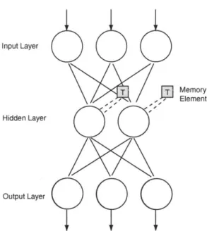
In order to process time dependent data and approximate the function of a state ma-chine, feedback mechanisms must be added to the neural network such that the architecture becomes recurrent. This can be accomplished by adding loops which allow the output of hidden layers to be stored from one cycle and then used in the calculation during the
subse-Input Layer
T -T Memory
'ee P Element
Hidden Layer
Output Layer
Figure 1-5: Multilayer perceptron with Elman-style memory elements. The memory ele-ments store the previous output of the neuron and feed this value back during the next cycle.
quent time steps as shown in Fig. 1-5. In this way, the output of the neural network acquires a state dependence. This modification to the MLP architecture was proposed by Elman and the network now bears his name [13]. Succeeding work has examined the computation power of Elman-style networks and their ability to simulate the operation of finite-state machines [14].
1.2
Prior Hardware Implementations of Neural Networks
Uti-lizing Optoelectronics
In the same way that much research has been done toward understanding and modeling how biological neural networks operate, other research has focused on how to artificially replicate these systems. Owning to the proliferation of integrated circuit technology, substantial work has been done to design neural network circuits in silicon [15, 16, 17, 18, 19, 20]. One of the key features is the ability to pack a large number of neurons onto a single chip which is possible due to the large scale integration available in modern process technology.
One of the challenges of designing neural network hardware that mimics the structure and operation of the brain is replicating the vast number of interconnections between
neu-rons. While the neurons of the brain communicate with an estimated 10,000 other neurons, resource limitations often limit physical neural networks to several orders of magnitude fewer interconnections. Optical communication between neurons, or planes of neurons, has been proposed as one solution to increasing the number of interconnections. A second idea for increasing the number of interconnections has been to connect every neuron in a network to a time-sharing bus such that every neuron receives the output of every other neuron. A brief review of two optically interconnected and one digital bus-based neural network will be presented in this section so as to provide a framework for, and preview the challenges of, the CONCOP.
1.2.1 MLP using Bench Optics at UCSD
The first system to be examined is a multilayer perceptron which uses free space optical communications for interlayer signaling. The system was first published by Krisnamoorthy, Yayla, and Esener in 1991 as a prototype to demonstrate the feasibility of using optical interconnects in neural processor applications [21, 22]. It combined both traditional ge-ometric optics and VLSI systems by using optical lenses to create scaled versions of the optical outputs which were then redirected to optoelectronic circuits for processing. This resulted in a large system which required the support of an optics lab for operation. The project was ultimately successful in that the system was able to consistently categorize horizontal and vertical lines after being properly trained. Since the system was developed at the University of California San Diego, it will be referred to as the UCSD MLP.
Architecture of the UCSD MLP
The UCSD MLP system is based on the Dual-Scale Topology Optoelectronic Processor
(D-STOP) architecture, previously developed for parallel matrix algebraic processing. This
architecture consists of arrays of neurons arranged in planes that consist of several subunits corresponding to the synapses, dendrites, and soma of a biological neuron. The distin-guishing feature of this architecture is the optics that are used to first demagnify and then replicate the array of optical outputs from the neurons such that full connectivity with the next layer is achieved.
A planar view of the system is shown in Fig. 1-6. The array of lenslets is used to focus
LI PBS fl+f2 L2 Demagnified Image CGH f2 B Neuron Array L3 B
Figure 1-6: Planar schematic of the UCSD MLP [22].
controlled such that an electrical input signal is converted to an optical form. The optical modulators are arranged in a 4 x 4 array such that the input plane essentially has 16 neurons. The 16 beams emanating from the modulators are then demagnified using the combination of lenses Li and L2. As expected, the demagnified image is inverted and rotated with respect to the output of the modulators. The computer generated hologram (CGH) and lens L3 is then used to replicate the demagnified image into a 4 x 4 array and focus it on the detectors of the array of neurons. As a result, each neuron receives the input from every neuron in the previous layer such that full connectivity is achieved. Since there are
16 neurons in the previous layer, each neuron in the hidden layer requires 16 detectors.
Examples of the input, demagnified, and replicated images are shown in Fig. 1-7.
INU 0 0 Input Image 0 0 N E 0 ed Demagnified Image NEEJOENE U HOC U U C El mu om on U U EJO U U C El Replicated Image Figure 1-7: Sample image at various stages of the UCSD MLP [22].
30 Lenslet Array
0
Modulator Array (Input Image)0
0
0
Hi Vlexc-t Vbias -- -- D5b ~--lout Vdd xc1 "nhinh
H
Synapse Circuit #1 D5 Synapse Circuit #2--- Nfn--- -- --- --- lout = a(ex t - inht) lexc C
Synapse Circuit #4 exc_4lu
~ec-
iht-S-napse Circuit #43a-n nt#
Figure 1-8: Circuit schematic of the UCSD MLP with four synapses and one fan-in unit [22].
Optoelectronics of the UCSD MLP
Each neuron in the hidden layer receives inputs from 16 neurons in the previous layer, and therefore requires 16 synapses to properly weight these inputs. The synapse circuitry is a hybrid topology which uses analog current mode multiplication coupled with digital weight storage. A schematic of the synapses circuits is shown in Fig. 1-8. The input to each synapse is a photodiode in the upper left of the diagram. The optical signal is converted to electrical current by the photodiode and then to an electrical voltage by the load transistor.
A series of buffers is used to insure rail-to-rail signal swing of the resulting voltage pulse.
The multiplication of the input signal and the corresponding weight is performed in a 5-bit multiplying digital-to-analog converter (MDAC) where the PMOS transistors connected to weights D1-D4 are scaled in a binary fashion such that the current sourced by the MDAC is proportional to the weight applied. The weight is stored as a 5-bit binary number where the most significant bit connected to D5 is a sign bit. Therefore D5 is used to steer the synapse current into either the excitatory or inhibitory wire depending on the sign.
The summation of the synapse output currents is divided into two stages through the addition of fan-in units. Four synapses are grouped together as shown in Fig. 1-8 into one
Fan-In Unit
#1
#2 Current PWM Output Output
#3 Integrator Converter Buffer
#4
Figure 1-9: Block diagram of the USCD MLP neuron [22].
fan-in unit, and then the four fan-in units are connected to the neuron of the neuron as shown in Fig. 1-9. The function of the fan-in unit is to find the net synapse current by taking the difference of the summed inhibitory and excitatory currents. The net current (either excitatory or inhibitory) is then passed to the neuron circuitry which sums the four fan-in currents and generates the output pulses.
UCSD MLP System Size and Performance
Since the UCSD MLP uses bench optics, discussions of system size have two components. The overall optical length of the system, found by summing the focal lengths of the various lenses in Fig. 1-6, was stated to be 60 cm. At the microelectronic level, the relevant size is found by considering the area occupied by the optoelectronics. Although this number was not directly reported by the authors, it was noted that a large area was consumed owning to the large area of the digital weight storage and the exponentially sized transistors of the
MDAC. However, the authors suggest that the area could be reduced in future versions
of the system by using analog weight storage and a suitably modified multiplier. In a 2-pm technology, a synapse density of 104 synapses/cm2 was believed possible with these modifications. Assuming 16 synapses per neuron, and that the neuron circuits consume trivial area, a neuron size of 1600 pm2 (40 pm x 40 pm) can be inferred. This compares with a previously published paper by the authors (published pre-silicon) where the neuron size was estimated at 25,000 pm2 (158 pm x 158 pm). Therefore, the actual neuron size
can be assumed to be between these two figures.
System performance was measured by training the network to categorize horizontal and vertical lines, meaning that the output of the system would indicate the presence of such a line in the 4 x 4 input array. A model of the system was assembled in software such that the network was trained out-of-the-loop. The model was presented with 20 noisy horizontal and vertical lines such that synaptic weights were determined. These were then
downloaded to the prototype hardware. Tests indicated that the system correctly identified any of the horizontal or vertical lines. The authors use a connections per second (CPS) metric to evaluate and compare the performance of the system. Connections per second refer to the number of connections between neurons that are made each second. Since the processing power of a neural network is related to the number of synapses and neurons, this is a quantitative means of performance evaluation. By measuring the minimum detectable output pulse to be 100 ns, the system was estimated to operate at a maximum of 640 million connections per second (CPS).
1.2.2 MLP for Robot Control at FSU
The second neural network processor to be considered was proposed by Maier, Becksteain, Clickhan, Erhard, and Fey in 1999, and will be referred to as the FSU MLP since it was developed at the Friedrich-Schiller-University in Jena, Germany [23, 24]. It is based on a multilayer perceptron architecture which uses digital optical communication between layers and digital computation in the neurons. It was developed as part of the control system for a hopping robot.
Architecture of the FSU MLP
The proposed processor consists of a traditional multilayer perceptron with one input layer, two hidden layers, and one output layer as shown in Fig. 1-10. The input layer is used only to generate the optical inputs for the first hidden layer, and thus no computation is
Input Hidden Hidden Output
Layer Layer #1 Layer-#2 Layer
1 //
0
40
40
o
Electronic Signals Optical Signalsn
performed. Likewise, the output layer is used to generate the output through the use of a linear transfer function. In contrast, the transfer function of each of the hidden layers is a non-linear sigmoid. By including two hidden layers, it is believed that the system can be trained to recognize any function.
All of the communication between neurons is performed using optoelectronic
transmit-ters and receivers that communicate between layers of the device. Since the processor is fully feed-forward, no lateral communication between neurons is provided. As in a typical MLP, the FSU MLP connects the output of each neuron in a plane with every neuron in the succeeding plane via one of that neuron's synapses. In order to accommodate back-propagation training algorithms, the processor uses 8-bit resolution for the optical links. Depending on whether parallel, serial, or more likely, a hybrid data transmission protocol is used, T (1 < T < 8) transmitters are included in each neuron such that
j
bits are sent in each transmission. For example, if four transmitters are used, two transmissions of 4 bits each are sent, such that the full 8 bits of the output are eventually transmitted.FSU MLP Neuron Structure
Each neuron of the FSU processor consists of three main components, specifically the input, electronic processing, and output blocks. The input block consists of an array of T x N receivers, where T represents the number of bits sent per transmission and N the number of neurons per layer. Therefore, each input block stores 8 x N bits of data in an array that represents the outputs of every neuron in the proceeding plane. In the actual system reported, T was set to eight such that the processor utilized fully parallel communications between planes. With a reported ten neurons (N = 10), this resulted in each input block requiring 80 receiving units. Given that the hidden layer also consisted of N neurons, a total of 800 receivers are required on a given layer of the device. Once the activation state has been received from the neuron in the previous layer, it is stored in local memory to await processing. For the system with ten neurons per plane, each neuron requires 80 bits of memory for the activation states plus eight bits for the bias for a total of 88 bits of memory. The electronic processing block resides between the input and output components and comprises the circuits required to emulate the thresholding performed by the neuron. The processing block is composed of several subsections including two memories (for both layer inputs and weights), a multiplier, an accumulator (for the output), and a look-up table based
0-Multiply O tu Input Memory Memory Sum -"--bit Weight
-8-bit -i and Bias
Memory
Figure 1-11: Digital processing block of the FSU MLP [23].
transfer function. A block diagram of the processing block is shown in Fig. 1-11. Operation of the block begins with the loading of the activation state and corresponding weight for a given neuron into the multiplier. This product is then added to the accumulator. After all of the products have been added to the accumulator, the resulting sum is used as the index into the transfer function look-up table. The result is stored in the output memory.
The simplest component of the neuron is the output block. This block consists of T transmitters (VCSELs) such that the activation state is transmitted to the neurons in the next layer. Since the system described used fully parallel communications, eight transmitters were needed per neuron such that each bit was sent in parallel to the next layer of neurons.
Optical Signal Analysis of the FSU MLP
The output block of one neuron and the input block of a neuron in the succeeding plane are arranged as shown in Fig. 1-12 such that a signal from the transmitting layer is received by many neurons in the receiving layer (where only four receiving neurons are shown for clarity). The optics necessary to split and redirect the incident optical beams are not discussed by
Sending Layer 881
11 8 1 8
~18
Receiving Layer
the authors, although a calculation to determine the theoretical optical fan-out is presented. The authors assume that 20 pA of current (Iph) is necessary to switch a gate in 0.8-pm
CMOS technology. By assuming a responsivity of 0.35 A/W (R) the power which must be
detected in a single receiver for the bit to be properly received is found to be 57 jiW.
phorep - 57 pW
(1.3)
optrec - 0.35A/W
Since the system was expected to use VCSELs for the transmitters, transmit power was assumed to be about 5 mW (Popt-trans). Therefore the fan-out, or the number of receivers capable of receiving a signal from a single transmitter, was calculated to be 87.
FOM < Pop~trans =87 (1.4)
Popt-rec
It should be noted that the authors assume perfect diffraction efficiency (7=100) of the holographic gratings.
System Size, Performance, and Scalability
The authors report an overall neuron size of 700,967 pm2 after completing layout in the 0.8-jim process. A breakdown of the area required for various components is shown in Table
1.1. The digital processing capabilities, specifically the adder and multiplier, required in
each neuron significantly increase the area consumed. Furthermore, the area estimates do not include routing resources or the additional 35% increase that occurred during timing optimization.
Since each layer of the system included 10 neurons, the size of each chip, or layer, was
32,000,000 im2 (5700 pm x 5700 pm). The authors did not report estimates for power
Component Chip Area (pm2
)
Weight Memory 152,741
Activation state memory 139,409
8 x 8 bit Pezaris multiplier 230,048 16-bit carry-ripple-adder 76,698
Transfer function 38,341
Table 1.1: Area of selected components for the FSU MLP [24].
consumption, nor did they report technical details of the holographic diffraction gratings used to direct the optical signals between layers. A brief discussion of the optimal number of hidden layers indicates that the system was expected to be scalable such that additional hidden layers could be added. Additionally, the system was designed such that each physical neuron could be multiplexed to emulate multiple logical neurons.
The reported connections per second (CPS) for the system when fully parallel commu-nications are used between the planes was 1 x 10¹⁰ CPS, assuming one logical neuron per physical neuron. The authors further claim that this performance compares favorably with the highest performing neural processor (which use analog computation) while maintaining the same accuracy of digital implementations, thereby outperforming these digital versions
by an order of magnitude.
The use of fully digital computation and communication insures a high-degree of ac-curacy in the computations throughout the system, but it comes with a price. Digital multipliers take considerable resources, both in terms of area and power consumption, such that the size of a single neuron would be large, and thus fewer neurons could be included in a plane of a given size. The size required for the standard cell components necessary to implement a single neuron was reported to be 700,967 pm2 (837 pm x 837 pm), a figure
which does not include the area needed for both intra-neuron and intrer-neuron routing [24].
1.2.3 Digital Bus-Based Neural Networks
Another approach to increasing the number of interconnections between neurons has been to use a bus-based architecture in which every neuron is connected to every other neuron in an arrangement resembling that of a Hopfield network. One such processor was developed at Hitachi and first published by Yasunaga et al. in 1989 [25, 26, 27, 28]. A representative model of the processor is shown in Fig. 1-13 which comprises four neurons. Full connectivity between the neurons is achieved by connecting each neuron output to the data bus which is then connected to the inputs of the other neurons.
Although the Hitachi processor provides full connectivity, only one synapse is needed per neuron due to the time-sharing characteristic of the data bus. The system operates like a synchronous system in that each neuron is assigned a time slice from the master clock cycle during which it places its output on the data bus. Therefore, each neuron only requires
Address Bus. -ControT --- , --- B-- --Synapse Sigmoid Table 'Neuron 'Data Bus
Figure 1-13: Hitachi bus-based architecture with four neurons. [27].
one synapse, but this synapse is used multiple times during a given cycle. An address bus is used to identify which neuron has control of the bus at a given point during the cycle.
Each of the neurons in the system is comprised of one synapse containing a local memory for storing addresses and weights as well as a multiplier for computing weighted activation states. Each neuron consists of an adder followed by a register for accumulating the sum of these weighted states as well as a second register for storing the previous sum, or activation state, of the neuron. A block diagram of a single synapse-neuron pair is shown in Fig. 1-14. Since the non-linear squashing function is not unique to a given neuron, it is integrated into the data bus of the entire system such that it does not need to be replicated locally.
A typical clock cycle of the processor begins with neuron NI placing its output from
register B on the data bus. Neurons N2:N4 simultaneously index into their local memories and load the weight corresponding to their connection with NI into their multiplier. (Since the memory required to store the addresses and weights grows as n2, the system actually only stores the top N weights, such that the concept of an 'address hit' is used. Therefore,
Address Weight
Sum A -+B +Bust
Address+ Data Multiply Registers
BusBu
Synapse Neuron
Figure 1-14: Neuron structure of the Hitachi bus-based architecture. [27].
![Figure 1-6: Planar schematic of the UCSD MLP [22].](https://thumb-eu.123doks.com/thumbv2/123doknet/14722778.570845/30.918.162.779.126.399/figure-planar-schematic-ucsd-mlp.webp)
![Figure 1-8: Circuit schematic of the UCSD MLP with four synapses and one fan-in unit [22].](https://thumb-eu.123doks.com/thumbv2/123doknet/14722778.570845/31.918.122.769.120.498/figure-circuit-schematic-ucsd-mlp-synapses-fan-unit.webp)
![Figure 2-1: The CONCOP being used for image enhancement and clutter removal. Adapted from [29].](https://thumb-eu.123doks.com/thumbv2/123doknet/14722778.570845/44.918.228.763.494.716/figure-concop-used-image-enhancement-clutter-removal-adapted.webp)