HAL Id: hal-00426822
https://hal.archives-ouvertes.fr/hal-00426822
Preprint submitted on 28 Oct 2009
HAL is a multi-disciplinary open access
archive for the deposit and dissemination of
sci-entific research documents, whether they are
pub-lished or not. The documents may come from
teaching and research institutions in France or
abroad, or from public or private research centers.
L’archive ouverte pluridisciplinaire HAL, est
destinée au dépôt et à la diffusion de documents
scientifiques de niveau recherche, publiés ou non,
émanant des établissements d’enseignement et de
recherche français ou étrangers, des laboratoires
publics ou privés.
Growth of (Ge,Mn) nanocolumns on GaAs(100): the
role of morphology and co-doping on magnetotransport
Matthieu Jamet, Ing-Song Yu, Thibaut Devillers, André Barski, Pascale
Bayle-Guillemaud, Cyrille Beigne, Johan Rothman, Vincent Baltz, Joel Cibert
To cite this version:
Matthieu Jamet, Ing-Song Yu, Thibaut Devillers, André Barski, Pascale Bayle-Guillemaud, et al..
Growth of (Ge,Mn) nanocolumns on GaAs(100): the role of morphology and co-doping on
magneto-transport. 2009. �hal-00426822�
Growth of (Ge,Mn) nanocolumns on GaAs(100): the role of morphology and
co-doping on magnetotransport
M. Jamet1 , I.-S. Yu1 , T. Devillers1 , A. Barski1 , P. Bayle-Guillemaud1 , C. Beigne1 , J. Rothman2 , V. Baltz3 , J. Cibert4 1INAC/SP2M, CEA-UJF, Grenoble, France
2
LETI/DOPT/LIR, CEA, Grenoble, France
3
INAC/Spintec, CEA-CNRS-UJF, Grenoble, France
4
Institut N´eel, CNRS-UJF, Grenoble, France (Dated: October 28, 2009)
Changing the morphology of the growing surface and the nature of residual impurities in (Ge,Mn) layers - by using different substrates - dramatically changes the morphology of the ferromagnetic Mn-rich inclusions and the magnetotransport properties. We obtained p-type layers with nanocolumns, either parallel or entangled, and n-type layers with spherical clusters. Holes exhibit an anomalous Hall effect, and electrons exhibit a tunneling magnetoresistance, both with a clear dependence on the magnetization of the Mn-rich inclusions; holes exhibit orbital MR, and electrons show only the normal Hall effect, and an additional component of magnetoresistance due to weak localization, all three being independent of the magnetic state of the Mn rich inclusions. Identified mechanisms point to the position of the Fermi level of the Mn-rich material with respect to the valence band of germanium as a crucial parameter in such hybrid layers.
PACS numbers: 75.50.Pp, 73.50.-h, 75.47.-m, 75.75.-c
Research on ferromagnetic semiconductors triggered enormous activity due to their potential use in spintron-ics [1, 2]. Up to now, efforts have mainly focused on diluted magnetic semiconductors (DMS) in which mag-netic atoms randomly substitute the host matrix atoms [3]. Their magnetic properties can be manipulated by electric fields making them suitable materials for spin-tronic applications provided that they can be made ferro-magnetic above room temperature. However DMS based on II-VI and III-V semiconductors still exhibit very low values of Curie temperature TC.
Many groups have reported TCvalues well above room temperature, along with remarkable magneto-transport and magneto-optical properties, in semiconductors doped with magnetic transition metals (TM). It is now admitted that these properties may be attributed to TM-rich ar-eas resulting from spinodal decomposition [4]. Such fea-tures have been theoretically predicted [5] and reported in (Ge,Mn) [6, 7, 8, 9], and in Cr and Fe-doped GaN [10, 11] or ZnTe [12]. In this field of intense materials re-search, goals are now: (i) controlling spinodal decomposi-tion to reproducibly stabilize high-TCTM-rich areas and tailor desirable magnetic properties, and (ii) enhancing the coupling with carriers to give rise to strong magneto-resistance (MR) or anomalous Hall effect (AHE).
In this paper, we demonstrate the fine control of spinodal decomposition in (Ge,Mn) films grown on GaAs(001) substrates. We focus on (Ge,Mn) because it is compatible with mainstream silicon technology, and spinodal decomposition leads to high TC values in lay-ers grown on Ge substrate. Growing (Ge,Mn) films on GaAs(001) semi-insulating (ρ > 107
Ωcm) substrates makes in-plane transport measurements easier, and con-stitutes a first step towards spin injection from (Ge,Mn) into a GaAs-based spin-LED [13]. Using different
sur-face preparations, we clearly identify the role of sursur-face morphology and the role of impurity diffusion from the substrate (either Ga or As atoms), on the nanocolumns growth, on one hand, and on the electrical properties, on the other hand. We thus address the major issue of the influence of co-doping (either n-type or p-type) on spinodal decomposition in group IV magnetic semicon-ductors, demonstrating a major influence on the shape of the Mn-rich precipitates. We also provide new hints to control and optimize magneto-transport propertie of the (Ge,Mn) films. We show that AHE and MR are not optimized simultaneously, and we propose a general pic-ture based on the electrical doping of the matrix and on the position of Fermi level in the precipitates with respect to the valence band of Ge.
(Ge,Mn) films were grown by low temperature Molec-ular Beam Epitaxy (MBE), using growth conditions as described in Ref. [6], with the substrate temperature Tg = 100◦C and deposition rate ∼ 0.2 ˚A.s−1. We have used two different methods to prepare the GaAs surface. In the first one, the native oxide was thermally desorbed from an epiready substrate, by raising the substrate tem-perature up to almost 600◦C. The (Ge,Mn) layers was grown directly on the resulting Ga-rich GaAs surface, which was rough as observed by RHEED. Such samples will be labelled Ga-(Ge,Mn). In the second case, As-(Ge,Mn) samples, a thin undoped GaAs buffer layer was grown first in a separate III-V system, protected with an amorphous As capping, and transferred in air to the IV-IV MBE machine. Desorbing the As capping layer at 200◦C results in a very flat, (2×4) reconstructed, As-rich surface. Samples grown on Ge substrates, labelled Ge-(Ge,Mn), constitute our reference samples.
Magnetization was measured using a Superconducting QUantum Interference Device (SQUID).
Magnetotrans-2 port properties (magnetoresistance and Hall effect) were
investigated using Hall bars defined by optical lithogra-phy, aligned along a < 110 > direction, of width 20 µm, with voltage probes separated by 140 µm.
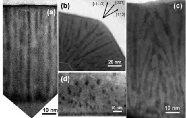
FIG. 1: TEM cross section of 80 nm thick layers : (a) Ge0.94Mn0.06grown at 100◦C after depositing a 40 nm thick
Ge buffer on GaAs(001) and (b) at 100◦C on the facetted
Ge surface. (c) Ga-Ge0.9Mn0.1 and (d) As-Ge0.98Mn0.02films
grown at 100◦C.
A typical morphology is that of long Mn-rich nanocolumns, growing normal to the substrate surface. On a Ge substrate [6] or on a Ge buffer layer grown on GaAs(001) (Fig. 1a), these nanocolumns are well aligned along the [001] growth direction. On a Ge buffer layer grown on a Ge(001) substrate with {113} facets obtained by anisotropic chemical etching in an H2O2 aqueous so-lution, Fig. 1b, they grow perpendicular to the facets. Finally, in Ga-(Ge,Mn) films, they are bent according to the initial surface roughness (Fig. 1c), and this results in a highly disordered pattern. This general picture fully agrees with 2D spinodal decomposition, driven by surface diffusion and aggregation of Mn atoms, with nucleation of Mn-rich areas taking place during the first stage of the growth [5]. As a consequence of this mechanism, the columns are always perpendicular to the growing surface.
FIG. 2: Temperature dependence of magnetization in (a) Ga-Ge0.9Mn0.1 and (b) As-Ge0.94Mn0.06: ZFC-FC curves at
0.015 T and magnetic remanence Mr after maximum field
cooling at 5 T. Inset: in (a), saturation magnetization at 2 T, and in (b), TEM image of a Ge3Mn5 cluster.
By contrast, in Fig. 1d, the As-(Ge,Mn) layers fea-ture randomly distributed Mn-rich precipitates. In ad-dition, a few Ge3Mn5 clusters already start to form, as evidenced by their typical Moir´e contrast (see inset of Fig. 2b). The same random distribution of nanoclus-ters is observed when increasing the nominal Mn content from 2% to 6% and 10% at Tg=100◦C, but for an increase of the average precipitate density and length along the growth direction. This suggests that the decomposition is of 3D character and mostly driven by nucleation.
Secondary Ion Mass Spectroscopy (SIMS, not shown) performed on the As−(Ge,Mn) samples evidences an As-rich topmost layer, extending over 3±1 nm below the sample surface and containing up to 6×10¹⁹
As cm−3, i.e., an integrated amount of almost 1 ML As. This is a consequence of the segregation of As atoms, initially present at the GaAs surface, during the growth of Ge, with a well-known surfactant effect [14]. Accordingly, as described below, the As-(Ge,Mn) films appear as n-doped: As atoms are shallow donors in Ge, and in this topmost layer they compensate p-type doping by substi-tutional Mn.
The presence of As near the surface of the growing layer offers a possible explanation for this change of character of the spinodal decomposition, from 2D to 3D. According to Ref. [15], Mn atoms are incorporated into germanium in a subsurface interstitial position, and further diffuse within the growth plane: this offers a mechanism for 2D spinodal decomposition [5]. Codoping with As changes the charge state of Mn atoms, thus reducing Coulomb repulsion and enhancing the effect of attractive Mn-Mn pair interaction, making the nucleation of Mn-rich pre-cipitates easier [4]. In addition to that mechanism, the presence of donors like As is expected to displace the equilibrium between interstitial Mn (another donor) and substitutional Mn (an acceptor), enhancing the amount of substitutional Mn (which form nucleation centers for further Mn aggregation [16]), and reducing the amount of interstitial Mn (thus decreasing the incorporation into already existing clusters). These different mechanisms induced by the presence of As conspire to favor a growth process dominated by nucleation, contributing to make the spinodal decomposition 3D.
A complete study of the magnetic properties will be published elsewhere [17]. All samples exhibit two [case of Ga-(Ge,Mn), Fig. 2a] or three [case of As-(Ge,Mn), Fig. 2b] magnetic phases, as evidenced from the tempera-ture dependence of the saturation magnetization Ms (in-set of Fig. 2) and the remanent magnetization Mr, and the ZFC-FC curves. They exhibit: (i) a strong para-magnetic signal with a 1/T temperature dependence at low temperature, attributed to Mn atoms diluted in the Ge matrix, and well fitted using a 3/2-Brillouin function [18]; (ii) a contribution attributed to the superparamag-netic Mn-rich nanocolumns or precipitates, with finite TC and blocking temperature TB; (iii) in As-(Ge,Mn) only,
a contribution from Ge3Mn5clusters with a broad range of blocking temperatures. A detailed analysis [17] of the Ga-(Ge,Mn) sample in Fig. 2a shows that 40±6% of the magnetic moments are in nanocolumns, with TC≈ 150 K and TB = 15±5 K, 1.0±0.1 µB/Mn, and an average magnetic moment of a nanocolumn 520±50 µB. For the As-(Ge,Mn) sample in Fig. 2b, we found that 52±3% of the magnetic moments are in the matrix, and 22±2% in the Mn-rich precipitates with TC ≈ 50 K, TB=15±5 K, 1.2±0.2 µB/Mn, and ≈100±20 µB per precipitate.
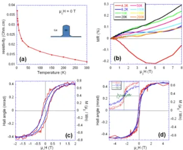
FIG. 3: Magnetotransport in Ga-Ge0.9Mn0.1, magnetic field
applied normal to the plane: temperature dependence of the zero-field resistivity (a), MR up to 8 T at different tempera-tures (b), and AHE (red) compared to magnetization (blue) at 2-3 K (c) and 4-5 K (d). Inset: AHE at 10, 100 and 150 K.
From the high field slope of the Hall effect, Ga-Ge0.9Mn0.1 films are p-type, with a hole density up to 3×10¹⁹
cm−3 at 300 K, comparable to what we gave as a lower bound (due to a strong AHE) of the hole density in Ge-(Ge,Mn). The resistivity (Fig. 3a) is of the insulating type (it was metallic in Ge-(Ge,Mn)). Mn was reported as a double acceptor in germanium, with acceptor levels 160 meV and 370 meV above the valence band edge [19] respectively. For such a deep acceptor, the Mott critical density is expected to be well in the 1020
cm−3 range, and for a measured density one order of magnitude lower we should observe a strongly activated conductivity [20]: we actually observe (Fig. 3a) a weak temperature depen-dence. We conclude that the Hall effect is not due solely to the holes from the Mn acceptors in the germanium matrix. This is possible if the Fermi level of the Mn-rich material forming the precipitates lies below the top of the valence band in germanium, so that no Schottky barrier, and even an accumulation layer, is formed around each precipitate. That induces the build-up of an electric field pattern around each nanocolumn, which drags holes to-wards the nanocolumn.
Then the magnetotransport properties can be under-stood as follows: (i) as the nanocolumns configuration is well below the percolation threshhold, holes have to prop-agate through the germanium matrix; that makes the basis of the conductivity; (ii) however, the electric field pattern drags the holes through the nanocolumns, where the conductivity is higher; applying a magnetic field sup-presses this effect, creating the geometrically enhanced orbital MR, or Extraordinary MR (EMR)[21] which we observed to be strong in Ge-(Ge,Mn) [6]; (iii) finally, the absence of Schottky barrier enhances the interaction of holes with Mn atoms in the nanocolumns, thus allowing a spin polarization and a strong AHE to appear [6].
In the Ga-(Ge,Mn) samples, we still observe the EMR (Fig. 3b), with the same temperature dependence as in Ref. [6], but much weaker (although much higher than classical Lorentz MR). This is readily explained by con-sidering the dependence of EMR on the carrier mobility (it scales as µ2
): as seen in Fig. 3a, the zero-field resistiv-ity ρ0in Fig. 3a is of the order of 10−2 Ω cm, so that the mobility is lower than in Ge-(Ge,Mn) by more than one order of magnitude, possibly due to the higher disorder and induced defects. Finally, at very low temperature, negative MR is observed, which may be due to spin disor-der scattering [22] on Mn atoms diluted in the Ge matrix (as typical in metallic DMS), or to GMR on the Mn-rich nanocolumns. In both cases, this effect is expected to be very weak; in addition the spin diffusion length of holes is very short due to spin-orbit coupling, making GMR on Mn-rich nanocolumns unlikely.
AHE in Ga-(Ge,Mn) nicely matches the magnetiza-tion of the nanocolumns (Fig. 3c-d). Again, the effect is weaker than in Ge-(Ge,Mn), by almost two orders of magnitude. This is expected from the lower mobility: it was pointed out in Ref. [23] that scattering on impuri-ties such as Ga atoms (SIMS measurements have indeed shown that Ga out-diffused from the GaAs substrate) partly suppresses the effect of skew scattering.
As-(Ge,Mn) films exhibit metallic n-type conductivity. This is clearly due to the presence of As donors in the topmost layer. Hence magnetotransport essentially mea-sures the properties of this 3 nm thick layer. We observe no AHE, as expected since spin-orbit scattering is small for electrons in the conduction band of germanium, and also because the same assumptions as above (Fermi level of precipitates lying below the top of the valence band) creates a high Schottky barrier for electrons.
MR is highly anisotropic (Fig. 4a): we show now that this is due to 2D weak localization in the As-doped layer, which vanishes when the field is applied in-plane (θ = 0). The isotropic part (Fig. 4c-d) will be analyzed later on.
The MR of non-interacting electrons in the 2D weak localization regime is ∆ρ/ρ ≈ −∆σ/σ = −A.f2[4eµ0Hsin(θ)Lφ/~] [24], where A = e2
/2π2~
σ2D(0), Lφ is the phase relaxation length, and the function f2(x) is defined in [24]. Here we neglect
4
FIG. 4: Magnetotransport in As-Ge0.94Mn0.06. (a) field
dependance and (b) temperature dependence of the MR anisotropy, for different orientations of the field; symbols are experimental data, solid line calculated. (c,d) MR and mag-netization as a function of the field applied in-plane.
the effect of spin-orbit coupling and the anisotropy of Lφ [17]. Fits in Fig. 4a were obtained with only two adjustable parameters: A = 4%, close to the value A = (6 ± 2)% calculated using the experimental value of the 2D conductivity at H = 0, and Lφ= 11.5 nm, large enough with respect to the thickness of the conducting layer to justify the use of the 2D regime of weak local-ization. Moreover, fits of the temperature dependence of the anisotropic MR (Fig. 4b) were obtained by simply writing Lφ=pDτφ, using the temperature dependence of the diffusion coefficient D for an n-doped degenerate semiconductor [25], and a temperature dependence of the phase relaxation time τφ∝ T−αwith α ≈1.7, similar to that obtained in [26] for Ge:Sb (α=1.5) and in [27] for Si-MOSFETs (α=1.6), and currently attributed to both electron-electron and electron-phonon collisions.
Turning back to the isotropic MR, Fig. 4c-d, it con-tains a negative contribution, which features two maxima at the coercive field of Mn-rich precipitates, and van-ishes above 50 K as does their magnetization. Hence, we tentatively ascribe it to tunneling MR (TMR) through the precipitates and the Schottky barriers formed around them. By analogy with spin injection from a ferromag-netic metal to a semiconductor [28], efficient spin injec-tion from the precipitate to the matrix requires an inter-face resistance provided by the Schottky barrier. This barrier must be high enough to prevent full spin relax-ation inside the precipitate but reasonably transparent to allow tunnel MR to occur.
To summarize, we have shown that surface
morphol-ogy and co-doping have major influence on spinodal decomposition in (Ge,Mn) films grown on GaAs(001) substrates. For films grown on Ga-rich rough sur-faces, we recovered 2D spinodal decomposition with bent nanocolumns. Electrical properties are similar to what we obtained on Ge(001) substrates except that the pres-ence of defects in the films leads to weaker positive MR and AHE. For films grown on As-rich flat surfaces, 3D spinodal decomposition is observed due to As co-doping and magnetotransport is dominated by TMR and weak localization, AHE is negligible. These results are consis-tent with the assumption that the Fermi level of Mn-rich precipitates lies in the valence band of the Ge matrix.
We thank A. Arnoult (LAAS, Toulouse) for providing As-capped GaAs substrates, T. Dietl and J. Pernot for fruitful discussions. This work was granted by the Agence Nationale pour la Recherche (project GeMO) and the Nanoscience Foundation in Grenoble (project IMAGE).
[1] A. H. MacDonald et al. , Nature Mater. 4, 195 (2005). [2] T. Dietl et al. , Semicond. Sci. Technol. 17, 377 (2002). [3] H. Ohno et al. , Science 281, 951 (1998).
[4] T. Dietl et al. , J. Appl. Phys. 103, 07D111 (2008). [5] K. Sato et al. , Jpn. J. Appl. Phys. 44, L948 (2005). [6] M. Jamet et al. , Nature Mater. 5, 653 (2006).
[7] D. Bougeard, S. Ahlers, A. Trampert, N. Sircar, G. Ab-streiter , Phys. Rev. Lett. 97, 237202 (2006).
[8] A. P. Li et al. , Phys. Rev. B 75, 201201(R) (2007). [9] T. Devillers et al. , Phys. Rev. B 76, 205306 (2007). [10] L. Gu et al. , J. Magn. Magn. Mater. 290-291, 1395
(2005).
[11] A. Bonanni et al. , Phys. Rev. Lett. 101, 135502 (2008). [12] S. Kuroda et al. , Nature Mater. 6, 440 (2007).
[13] R. Fiederling et al. , Nature 402, 787 (1999).
[14] A. Leycuras et al. , Appl. Phys. Lett. 66, 1800 (1995). [15] W. Zhu et al. , Phys. Rev. Lett. 93, 126102 (2004). [16] W. Zhu, Z. Zhang, E. Kaxiras , Phys. Rev. Lett. 100,
027205 (2008).
[17] I.-S. Yu et al. , to be published.
[18] T. C. Schulthess et al. , J. Appl. Phys. 89, 7021 (2001). [19] H. H. Woodbury et al. , Phys. Rev. 100, 659 (1955). [20] P. Achatz et al. , Appl. Phys. Lett. 92, 072103 (2008). [21] S. A. Solin et al. , Science 289, 1530 (2000).
[22] F. Matsukura, H. Ohno, A. Shen, Y Sugawara , Phys. Rev. B 57, R2037 (1998).
[23] Y. D. Park et al. , Science 295, 651 (2002).
[24] B. L. Altshuler and A. G. Aronov, in Electron - Electron Interactions in Disordered Systems, edited by A. L. Efros and M. Pollak (North-Holland, Amsterdam, 1985), p. 1.
[25] S. M. Sze, Physics of Semiconductors Devices (Wiley, New York, 1981).
[26] T. A. Polyanskaya et al. , Sov. Phys. JETP Lett. 34, 361 (1981).
[27] M. J. Uren et al. , J. Phys. C 14, L395 (1981).