HAL Id: tel-00351281
https://tel.archives-ouvertes.fr/tel-00351281
Submitted on 8 Jan 2009HAL is a multi-disciplinary open access archive for the deposit and dissemination of sci-entific research documents, whether they are pub-lished or not. The documents may come from teaching and research institutions in France or abroad, or from public or private research centers.
L’archive ouverte pluridisciplinaire HAL, est destinée au dépôt et à la diffusion de documents scientifiques de niveau recherche, publiés ou non, émanant des établissements d’enseignement et de recherche français ou étrangers, des laboratoires publics ou privés.
Signatures de l’injection optique et électrique de charges
dans des monocristaux de rubrene
Nripan Mathews
To cite this version:
Nripan Mathews. Signatures de l’injection optique et électrique de charges dans des monocristaux de rubrene. Matériaux. Université Pierre et Marie Curie - Paris VI, 2008. Français. �tel-00351281�
THESE DE DOCTORAT DE L’UNIVERSITE PARIS 6
Spécialité : Chimie Moléculaire
Présentée par
M. Nripan MATHEWS
Pour obtenir le grade de
DOCTEUR DE L’UNIVERSITE PARIS 6
Signatures of optically and electrically injected charges in rubrene
single crystals
Soutenue le 19 septembre 2008 devant le jury composé de :
Dr Denis FICHOU
Directeur de thèse
Pr Max MALACRIA
Examinateur
Dr Dominique VUILLAUME
Rapporteur
Dr Alberto MORPURGO
Rapporteur
Pr Subodh MHAISALKAR
Examinateur
Pr Freddy BOEY
Examinateur
Thèse préparée au:
CEA Saclay, LRC Nanostructures et Semi-Conducteurs Organiques CNRS-CEA-UPMC
Abstract
Organic single crystals are of particular fundamental interest as tools in probing the intrinsic electrical properties and the upper limit of performance for a given organic semiconducting molecule devoid of disorder. Rubrene single crystals are of particular interest in the field of organic electronics due to the high levels of charge carrier mobilities measured in transistors constructed of the same. In this thesis, we explore the properties of rubrene single crystal transistors.
The photocurrent properties of rubrene single crystals are measured in ‘air-gap’ transistors whose unique structure allows the measurement of photocarrier dynamics without the influence of a dielectric that can act as a source for traps. This structure has allowed us to identify phenomenon like persistent photoconductivity associated with the creation of oxygen related traps on the rubrene surface. Transient studies of the photocurrent reveal the presence of bimolecular recombination of the charge carriers. In addition, we have also performed optical spectroscopy studies including Raman spectra measurements which revealed the presence of endoperoxide related signature on the surface of the crystal while also confirming the low levels of intermolecular coupling present between the molecules.
We have also explored the extrinsic factors that determine the surface conductivity of the rubrene crystal, particularly the presence of oxide related compounds on the surface of the crystal using XPS and photoluminescence measurements. The impact of photo-oxidation of the rubrene crystal on the surface conductivities were evaluated by a novel experiment involving the gradual photo-oxidation of the rubrene surface using a focussed laser. The creation of a deep acceptor state that can trap electrons indicates that the electrical properties of the rubrene surface like high unipolar p-type
conductivity and photoconductivity may be modulated by the presence of these oxygen induced states.
Acknowledgements
The past three years spent in pursuing a PhD has taught me many valuable lessons and
brought me in contact with many people who have been a pleasure to work with and who
have affected my life in many ways. It is my great pleasure to acknowledge them here.
First of all, I would like to thank Dr Denis Fichou for having supervised my thesis at
CEA-Saclay. Your perspective and knowledge of organic electronics, as well as your
advice on how to manage research is greatly appreciated. I will remember your advice
about always ‘putting things in the box’. I would also like to thank Prof Subodh
Mhaisalkar for having co-supervised me. Your enthusiasm, ideas and energy during the
past three years have been instrumental in ensuring the completion of this thesis. Your
flexibility and patience was very helpful in trying to balance work between Singapore
and France.
I also gratefully acknowledge the help and collaboration from Dr. Vitaly Podzorov and
Dr. Etienne Menard. I am very thankful for the discussions and suggestions regarding my
work. My gratitude also goes to Dr Tripathy and Mr Keke Zhang for help with the
measurements for Raman spectra and gas sensing respectively.
My PhD journey would have been a lot harder if it was not for the support, help and
sympathetic ears provided to me by my friends and colleagues in both France and
Singapore. My heartfelt as well as ‘stomach felt’ appreciation go to Ludovic, Camille,
Claudia, Odile, Alexandre, Giulia, Luc, Vadym, Vladymyr and Stephane. A special thank
you also goes to Alexander Marchenko for his help during my time in France. Spending
time in France has been a wonderful experience because of all you.
I am also grateful to all my friends in Singapore. At the polymer electronics group in
Nanocluster, I would like to show gratitude to Wei Lin for being the sounding board for
many of my ideas and for help with the experimentation, as well as Willy, Anup, Zong
Bin, Tommy, Ju Nie, Phoebe, Vera and Victor. You all have been instrumental in
creating a good fun filled environment to work in and for keeping my spirits high when
things do not go well.
Last but definitely not the least; I would like to thank my family. I greatly acknowledge
my parents who have supported me through all the decisions I have made and whose
concern and love for me gives me hope and encouragement every day. Thank you my
brother and sister-in-law for your patience and love as well.
Table of Contents
Page Abstract I Acknowledgements III Table of Contents VI List of Figures IX List of Tables XV 1. General Introduction 1 1.1 Thesis overview 4 1.2 References 62. Electronic properties of molecular crystals 9
2.1 Organic semiconducting molecules 10
2.2 Intermolecular interaction 12
2.3 Charge transport characteristics of organic single crystals 16
2.3.1 Band like transport 16
2.3.2 Influence of traps 18
2.3.3 Polaron transport 21
2.4 References 26
3 Free-space dielectric field effect transistors 31
3.1 Single crystal growth 32
3.2.1 Elastomeric transistor stamps 36
3.3 Air-gap stamps 37
3.3.1 Fabrication of air-gap stamps 38
3.4 Working principle of field effect transistors 39
3.5 Contact effects in transistors 44
3.6 References 49
4 Photoconductivity in rubrene single crystals 53
4.1 Photoexcitation picture in organic molecular crystals 54
4.2 Excitons 55
4.2.1 Frenkel excitons 56
4.2.2 Wannier-Mott excitons 56
4.2.3 Charge-transfer excitons 57
4.3 Basic concepts of photoconductivity 59
4.4 Transient photoconductivity 61
4.4.1 Monomolecular recombination 62
4.4.2 Bimolecular recombination 63
4.5 Steady state photoconductivity measurements in rubrene transistors 64
4.6 Photocurrent transients measured under pulsed illumination 73
4.7 References 79
5 Optical Characterisation of rubrene crystals 82
5.1 Absorption and luminescence in Rubrene 83
5.1.1 Theory 83
5.1.2 Absorption spectra of rubrene solution and crystals 85
5.2 Photoluminescence Spectroscopy 88
5.2.2 Luminescence in conjugated systems 89
5.2.3 Luminescence in rubrene solutions and crystal 91
5.3 Raman spectroscopy 94
5.3.1 Theory 94
5.3.2 Experimental 96
5.3.3 Rubrene Single Crystal Raman spectra 98
5.3.4 Raman spectra for the different facets of the crystal 104
5.3.5 Temperature dependency 104
5.3.6 Electric field dependencies 106
5.4 References 109
6 Extrinsic effects on charge conducting properties of rubrene 112
6.1 Common extrinsic effects in organic devices 112
6.2 Oxidation of rubrene in solution 115
6.3 Photoluminescence measurements on rubrene crystal surface 117
6.4 X-ray Photoelectron Spectroscopy 118
6.5 In-situ photo-oxidation measurements 120
6.6 Source of conductivity modulation induced by oxygen effects 122
6.7 Influence of nitrogen dioxide on rubrene transistors 122
6.8 References 126
List of Figures
Figure 1.1: Molecular structure of rubrene showing the tetracene backbone and the four
pendant phenyl rings in a twisted configuration ………....3
Figure 2.1: Chemical structure of some widely used semiconducting organic
polymers………...9
Figure 2.2: Chemical structure of some well known small molecule semiconductors…10
Figure 2.3: Creation of delocalized π electron system in a benzene molecule-the building
block of the acene group ………...11
Figure 2.4: Energy levels of (single) ionic states of the acenes from benzene to pentacene
for the free molecule in the gas (g) state (left, solid lines), and for the crystal (c) (right,
double lines), defined by the electron-binding energy relative to the vacuum level. I
gand
I
cstand for ionization energies for gas phase and crystalline phase, A
gand A
cfor electron
affinities for gas and solid phases, P
eand P
hfor electron and hole polarization energies
respectively………..…12
Figure 2.5: A top view of the ab- plane crystal structure of rubrene. The herringbone
configuration is apparent………..…14
Figure 2.6: (Left) Molecular packing in the rubrene crystal. Blue arrow indicates the
direction of highest mobility (Right) Charge carrier mobility anisotropy on the surface of
rubrene crystal……… 15
Figure 2.7: Electron and hole mobilities in the a-direction of highly purified naphthalene
crystals for different field strengths……….17
Figure 2.8: Temperature dependent conductivity measurements on the rubrene transistor
showing the trap limited regime at low temperatures and intrinsic regime at higher
temperatures……….20
Figure 2.9: Temperature dependence of the carrier mobility for six different gate
dielectrics. The temperature dependence evolves from metallic-like to insulator-like, as
the dielectric constant is increased………..24
Figure 3.1: Schematic of the PVT crystal growth………...32
Figure 3.2: Transistor fabrication by lamination of an organic crystal against the
transistor stamp. Initiating contact between the two surfaces results in a wetting front that
progresses across the semiconductor-stamp interface until the entire crystal is in intimate
contact with the stamp……….36
Figure 3.3: Schematic illustration of the construction of organic single crystal transistors
with free space gate dielectrics………38
Figure 3.4:a) Idealized energy level diagram of an organic TFT at V
G= 0 and V
D= 0.
(b-e) Demonstrate the principle of field effect transistor operation for the case of (b) electron
accumulation, (d) transport, (c) hole accumulation, and (e) transport………41
Figure 3.5: Output characteristics of a rubrene air-gap transistor (L=300 µm, W=1000µ m)
measured at 295K and 210K illustrating contact effects……….44
Figure 3.6: Mobility dependence on temperature for saturation and linear regime
indicating the influence of the contacts. Activation energy extracted using simple
Arrhenius dependence shows E
a=0.059eV for saturation regime, 0.1eV for linear
regime………..47
Figure 4.1: Energy band diagrams of photoexcitations in organic semiconductors
according to semiconductor band model (left) and molecular exciton model (right)….54
Figure 4.2: Illustration of the charge delocalization in Wannier-Mott and Frenkel
excitons………57
Figure 4.3: Descriptions of photoexcitations in organic molecular crystals………58
Figure 4.4: Simplest setup for measuring photoconductivity………. 60
Figure 4.5: Illumination configuration during phototransistor measurements…………65
Figure 4.6: Output characteristics of a representative rubrene transistor in dark and under
illumination showing clear photocurrent effects………..66
Figure 4.7: Excess carrier accumulation at the channel due to photogeneration expressed
as a shift in threshold voltage………67
Figure 4.8: Hysteresis effects in the transfer characteristics caused due to
illumination………....69
Figure 4.9: Persistent photoconductive effects created on illumination………70
Figure 4.10: Photoluminescence spectra proving the presence of oxygen related band
states on rubrene surface………71
Figure 4.11: Representative photocurrent response under pulsed illumination…………72
Figure 4.12: Non exponential behaviour of photocurrent decay eliminating
monomolecular recombination at work……….…74
Figure 4.13: Optical power dependence on photocurrent transient………...76
Figure 4.14: Gate voltage variation of photocurrent transients……….77
Figure 5.1: Possible de-excitation pathways of excited molecules………...83
Figure 5.2: Absorption spectrum of rubrene solution in cyclohexane………..85
Figure 5.1: Rubrene molecule with the L, M, N molecular axes defined……….86
Figure 5.3: Schematic illustration of the main electronic configurations contributing to
the ground state S
0and the lowest singlet excited states S
1and S
2in the case of
octatetraene………89
Figure 5.6: Luminescence spectra of rubrene solution(excited at 254 nm)………..91
Figure 5.4: Photoluminescence spectra measured on the different facets of the rubrene
crystal. Inset shows the ab plane result in more detail………..92
Figure 5.5: Schematic illustration of the Raman measurement setup utilized…………..97
Figure 5.6: Geometrical structure of rubrene molecule extracted from single crystal
diffraction………..98
Figure 5.7: Representative room temperature Raman spectra measured on the surface of
Rubrene crystals………..100
Figure 5.11: Exploration of the different facets of the rubrene crystal indicating no
dependency on the Raman spectra………..104
Figure 5.12: Raman intensities for the two strongest modes measured at 79K and
300K………105
Figure 5.13: Insensitivity to applied electric field………...………107
Figure 6.8: Absorption spectra of rubrene solution measured over time indicating the
reduction in rubrene concentration over time due to oxidation………...116
Figure 6.9: Fluorescence measurements indicative of the loss of conjugation associated
with rubrene……… 116
Figure 6.10: Photoluminescence spectra of rubrene crystals stored in ambient conditions
indicating presence of an additional peak at 650nm………....118
Figure 6.4: XPS spectrum of the rubrene crystal surface with an oxygen peak indicative
of the presence of rubrene peroxide………..…..120
Figure 6.5: Surface current measured over time during spatial scan. Inset shows a blown
up view of the current profile clearly identifying the time spent at each point………...121
Figure 6.6:Log-scale transfer characteristic of the identical rubrene single crystal OFET
under different NO2 concentration at Vd=-60 V……….123
List of Tables
Table 5.1 : Bond lengths and angles in rubrene molecule……….98
Table 5.2: Comparison of theoretically calculated Raman modes to experimentally
measured Raman modes in this experiment and in the literature………....101
Table 5.3: Normalised intensities for different incident polarization showing B
gvariation………...103
Table 5.4: Peak positions for rubrene modes at 300K and 79K………..106
.
General Introduction
Chapter 1
General Introduction
The use of organic materials in electronics has been historically in the important role of photoresists that act as stencils in the lithography process for defining features on inorganic semiconductors like silicon and gallium arsenide or as encapsulates of the finished electronic devices. In the past decade or so, there has been a burst in research activities which explore the use of organic materials as the active component of the device. The interest in the field of organic electronics has been widely growing since the fabrication of the first field-effect transistors (FETs) based on polymer and small-molecule semiconductors 1-5. The fabrication of the first all ‘plastic’ transistors were an important step in revealing the potential of organic electronics6, 7.Other organic devices fabricated include light emitting diodes (OLEDs)8-10, photovoltaic cells11-13, waveguides14 and organic lasers15. Organic transistors who are the workhorses of this field are especially interesting since they can serve as the main components in cheap and flexible electronic circuits with applications in displays, sensors and radio frequency identifications tags (RF-IDs) 16-29. The main advantage of using organic semiconductors for electronics is their ability to be processed from solution at room temperatures making them ideal for low area, low cost, large volume manufacturing processes like printing as well as ink-jetting. Another important advantage of using organic materials is that their properties like ionization potential can be tailored by varying their molecular structure, either by changing the degree of conjugation in the polymer or by the introduction of electronically active substituents30, 31.
In general, organic semiconductors consist of π conjugated structures which allows for delocalization of electrons along the length of the molecule. They are wide band gap
General Introduction
semiconductors with band gaps in the range of 2-3eV and can normally be classified into two families: polymers and small molecules. During the fabrication of active devices, small molecule organic semiconductors are thermally evaporated, forming a polycrystalline active layer whose properties are determined by surface treatment, temperature, material purity, as well as testing and deposition vacuum conditions32-34.The changes caused in film growth and morphology like varying crystallinity, microstructure, molecular packing and alignment are manifested in the mobility values. Even for devices with the same organic active layer, reported results often vary over an order of magnitude. In addition to the inconsistency of basic performance parameters, variations in morphology and ‘orientation averaging’ will mask properties intrinsic to molecular arrangement, such as electrical anisotropy.
Crystals made of organic semiconductors play an important role in the study of the fundamental properties of the molecules35-37. Single crystals are a useful tool in probing the intrinsic electrical properties and perhaps the upper limit of performance for a given organic semiconducting molecule. In order to link molecular functionality and crystal microstructure to their optical and electrical properties, it is crucial that variation in both overall molecular order and device quality are minimized or eliminated. The use of a single crystal of organic material addresses this by providing near-perfect order over its entirety, which is often centimetres in size. In particular, they have developed from a tool useful for simply gauging the upper limit of thin-film performance into a powerful method for examining both device physics and the intrinsic transport properties of semiconductor materials. In addition, newly developed patterning techniques for single crystals – by both vapourand solution methods38-40 – suggest that organic transistors based on single crystals may have potential as a viable method for hands-free circuit fabrication with the highest performance organic semiconductors available.
General Introduction
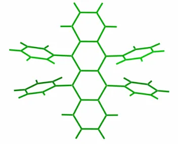
Figure 1.1: Molecular structure of rubrene showing the tetracene backbone and the four pendant phenyl rings in a twisted configuration
Among the various crystals prepared from small molecules, rubrene single crystals are of special interest. The rubrene molecule (5, 6, 11, 12-tetraphenyl tetracene) is a relatively small aromatic hydrocarbon consisting of a backbone of four fused benzene rings (tetracene) with four substituted phenyl rings as shown in Figure 1.1. Due to the bulky nature of the sidegroups, there is a large torsion angle 41between the phenyl rings and the tetracene backbone in rubrene (85°), which strongly reduces any mixing of the molecular orbitals between the backbone and the side groups. This in turn implies that the HOMO and LUMO levels of the rubrene and tetracene molecules are similar42. Rubrene single crystals are of particular interest in the field of organic electronics due to the high hole mobilities recorded in this material43. The development of various fabrication techniques particularly the “air-gap” technique allows a non invasive study of the semiconductor crystal surface due to the absence of the semiconductor-dielectric interface44. Our group observed unipolar conduction of holes under illumination through scanning tunneling studies on the surface of rubrene crystals.
In this thesis, we report the characteristics of rubrene single crystal field-effect transistors (SCFETs) fabricated using the “air-gap” technique. In addition, we explore photocurrent measurements in the steady state and in the transient state in this conformation. The “air-gap” technique allows us to study the direct photocurrent response of the rubrene crystal transistors
General Introduction
without the influence of a dielectric. The source of the electronic properties of rubrene is explored by the characterization of the single crystal by photoluminescence as well as by Raman scattering measurements. Finally, extrinsic factors that influence the surface conductivity of rubrene single crystals are explored.
1.1 Thesis overview
The following chapter introduces the reader to the various concepts regarding organic semiconductors and molecular crystals. The electronic properties of the crystals will be explored including the influence of the molecular structure and the intermolecular interactions. The charge transport characteristics of molecular crystals are explored and concepts relating to band like transport and polaron transport are introduced.
Chapter 3 deals with the fabrication and electrical characteristics of free-space dielectric transistors as well as the details of the physical vapor transport growth process of the organic crystals. The general principles behind the working of a field effect transistor are described as well. Contact effects and their dependence on the apparent mobility values measured in the transistors are briefly explored through temperature dependent measurements.
The steady-state and transient photocurrents measured in rubrene crystals in the transistor configuration are described in Chapter 4. The steady state measurements have revealed oxygen induced trap states on the surface of the rubrene crystal as evidenced by the observation of persistent photoconductivity in these samples. Transient photocurrents on the other hand has shown bimolecular recombination of the induced charge carriers which can be modulated by increased carrier densities induced by optical power as well as gate electric field.
Chapter 5 delves in to the various optical and vibrational characterizations performed on the rubrene crystal in order to explain the electrical properties of rubrene crystal. Raman
General Introduction
measurements on the surface of the crystal have not been able to detect intermolecular coupling, but may have revealed the presence of rubrene peroxide on the surface.
Finally chapter 6 explores the extrinsic factors influencing surface conductivities of rubrene crystals. This chapter details the various experiments performed to detect the presence of rubrene endoperoxide on the surface of the crystal as well as its influence on the charge transport properties of the rubrene crystal surface.
General Introduction 1.3 References
1. F. Ebisawa, T. Kurokawa and S. Nara, Journal of Applied Physics, 1983, 54, 3255-3259.
2. A. Tsumura, H. Koezuka and T. Ando, Applied Physics Letters, 1986, 49, 1210-1212. 3. A. Assadi, C. Svensson, M. Willander and O. Ingana?s, Applied Physics Letters, 1988,
53, 195-197.
4. K. Kudo, M. Yamashina and T. Moriizumi, Jpn. J. Appl. Phys., 1984, 23, 130-130. 5. G. Horowitz, D. Fichou, X. Peng, Z. Xu and F. Garnier, Solid State Communications,
1989, 72, 381-384.
6. F. Garnier, G. Horowitz, X. Peng and D. Fichou, Advanced Materials, 1990, 2, 592-594.
7. X. Peng, G. Horowitz, D. Fichou and F. Garnier, Applied Physics Letters, 1990, 57, 2013-2015.
8. T. W. Kelley, P. F. Baude, C. Gerlach, D. E. Ender, D. Muyres, M. A. Haase, D. E. Vogel and S. D. Theiss, Chemistry of Materials, 2004, 16, 4413-4422.
9. L. S. Hung and C. H. Chen, Materials Science and Engineering R: Reports, 2002, 39. 10. B. W. D'Andrade and S. R. Forrest, Advanced Materials, 2004, 16, 1585-1595.
11. P. Peumans, A. Yakimov and S. R. Forrest, Journal of Applied Physics, 2003, 93, 3693-3723.
12. C. W. Tang, Applied Physics Letters, 1986, 48, 183-185.
13. G. Yu, J. Gao, J. C. Hummelen, F. Wudl and A. J. Heeger, Science, 1995, 270, 1789-1791.
14. W. Geis, R. Sinta, W. Mowers, S. J. Deneault, M. F. Marchant, K. E. Krohn, S. J. Spector, D. R. Calawa and T. M. Lyszczarz, Applied Physics Letters, 2004, 84, 3729-3731.
15. M. A. Baldo, R. J. Holmes and S. R. Forrest, Physical Review B - Condensed Matter
and Materials Physics, 2002, 66, 353211-3532116.
16. H. Klauk, D. J. Gundlach, J. A. Nichols and T. N. Jackson, IEEE Transactions on
Electron Devices, 1999, 46, 1258-1263.
17. J. A. Rogers, Z. Bao, K. Baldwin, A. Dodabalapur, B. Crone, V. R. Raju, V. Kuck, H. Katz, K. Amundson, J. Ewing and P. Drzaic, Proceedings of the National Academy of
General Introduction
18. H. Sirringhaus, T. Kawase and R. H. Friend, MRS Bulletin, 2001, 26, 539-543.
19. C. D. Dimitrakopoulos and P. R. L. Malenfant, Advanced Materials, 2002, 14, 99-117. 20. H. E. A. Huitema, G. H. Gelinck, J. B. P. H. Van Der Putten, K. E. Kuijk, C. M. Hart,
E. Cantatore and D. M. De Leeuw, Advanced Materials, 2002, 14.
21. P. F. Baude, D. A. Ender, M. A. Haase, T. W. Kelley, D. V. Muyres and S. D. Theiss,
Applied Physics Letters, 2003, 82, 3964-3966.
22. M. Kitamura, T. Imada and Y. Arakawa, Japanese Journal of Applied Physics, Part 1:
Regular Papers and Short Notes and Review Papers, 2003, 42, 2483-2487.
23. G. H. Gelinck, H. E. A. Huitema, E. V. Veenendaal, E. Cantatore, L. Schrijnemakers, J. B. P. H. Van Der Putten, T. C. T. Geuns, M. Beenhakkers, J. B. Giesbers, B. H. Huisman, E. J. Meijer, E. M. Benito, F. J. Touwslager, A. W. Marsman, B. J. E. Van Rens and D. M. De Leeuw, Nature Materials, 2004, 3, 106-110.
24. V. Subramanian, P. C. Chang, J. B. Lee, S. E. Molesa and S. K. Volkman, IEEE
Transactions on Components and Packaging Technologies, 2005, 28, 742-747.
25. L. Torsi and A. Dodabalapur, Analytical Chemistry, 2005, 77.
26. S. Lee, B. Koo, J. G. Park, H. Moon, J. Hahn and J. M. Kim, MRS Bulletin, 2006, 31, 455-459.
27. M. Muccini, Nature Materials, 2006, 5, 605-613.
28. R. Rotzoll, S. Mohapatra, V. Olariu, R. Wenz, M. Grigas, K. Dimmler, O. Shchekin and A. Dodabalapur, Appl. Phys. Lett, 2006, 88, 123502.
29. L. S. Zhou, A. Wanga, S. C. Wu, J. Sun, S. Park and T. N. Jackson, Appl. Phys. Lett, 2006, 88, 083502.
30. G. Padmanaban and S. Ramakrishnan, Journal of the American Chemical Society, 2000, 122, 2244-2251.
31. P. F. Van Hutten, V. V. Krasnikov and G. Hadziioannou, Accounts of Chemical
Research, 1999, 32, 257-265.
32. Z. T. Zhu, J. T. Mason, R. Dieckmann and G. G. Malliaras, Applied Physics Letters, 2002, 81, 4643-4645.
33. M. M. Ling and Z. Bao, Chemistry of Materials, 2004, 16, 4824-4840.
34. D. Li, E. J. Borkent, R. Nortrup, H. Moon, H. Katz and Z. Bao, Applied Physics
Letters, 2005, 86.
35. M. Pope and C. E. Swenberg, Electronic Processes in Organic Crystals and Polymers, 2nd edn., Oxford University Press, New York, 1999.
General Introduction
36. C. Reese and Z. Bao, Materials Today, 2007, 10, 20-27.
37. E. A. Silinsh, Organic Molecular Crystals: their Electronic States, 1st edn., Springer-Verlag, Berlin, 1980.
38. A. L. Briseno, J. Aizenberg, Y. J. Han, R. A. Penkala, H. Moon, A. J. Lovinger, C. Kloc and Z. Bao, Journal of the American Chemical Society, 2005, 127, 12164-12165. 39. A. L. Briseno, S. C. B. Mannsfeld, M. M. Ling, S. Liu, R. J. Tseng, C. Reese, M. E.
Roberts, Y. Yang, F. Wudl and Z. Bao, Nature, 2006, 444, 913-917.
40. A. L. Briseno, R. J. Tseng, M. M. Ling, E. H. L. Falcao, Y. Yang, F. Wudl and Z. Bao, Advanced Materials, 2006, 18, 2320-2324.
41. I. Bulgarovskaya, V. Vozzhennikov, S. Aleksandrov and V. Belsky, Latv. PSR Zinat.
Akad. Vestis, Khim. Ser., 1983, 53.
42. D. A. Da Silva Filho, E. G. Kim and J. L. Bre?das, Advanced Materials, 2005, 17, 1072-1076.
43. V. Podzorov, E. Menard, A. Borissov, V. Kiryukhin, J. A. Rogers and M. E. Gershenson, Physical Review Letters, 2004, 93, 086602-086601-086602-086604. 44. E. Menard, V. Podzorov, S. H. Hur, A. Gaur, M. E. Gershenson and J. A. Rogers,
Electronic properties of molecular crystals
Chapter 2
Electronic properties of molecular crystals
Organic semiconductor molecules can be broadly classified into two families: polymers and small molecules. Polymeric molecules typically have high molecular weights and are relatively easy to process from solution and are present as amorphous or partially crystalline in the solid-state. Among the many polymers in this category, thiophene based polymers are notable for their higher electrical performance. Polymers like, Poly (3-hexylthiophene) (P3HT)1-5 , polyquarterthiophenes (PQT)6 , poly(9,9-dioctylfluorene-co-bithiophene) (F8T2)7 and poly(2,5-bis(3-alkylthiophen-2-yl)thieno[3,2-b]thiophenes) (PTTT) 8fall into this category of compounds.
S S S S C6H13 C6H13 C6H13 C6H13 n S S S S C12H25 C12H25 n C8H17 H17C8 S S n n S C14H25 S S S H25C14 P3HT PQT-12 F8T2 PTTT-14
Figure 2.1: Chemical structure of some widely used semiconducting organic polymers
Small molecules on the other hand have low molecular weights and are normally deposited by thermal evaporation. They normally consist of acenes like pentacene, tetracene, anthracene9-17 as well as oligomers like quarterthiophene, sexithiophene18-22.
Electronic properties of molecular crystals S S S S S S S S S S Pentacene Tetracene Anthracene Quarterthiophene Sexithiophene
Figure 2.2: Chemical structure of some well known small molecule semiconductors
The charge transport properties of the molecules and polymers mentioned above are determined by the individual energy levels of these molecules as well as the level of interaction between them which is mediated by intermolecular distances and the extent of the electron cloud overlap. Sections 2.1 and 2.2 introduce the molecular and intermolecular determinants of charge conducting behaviour in organic devices.
2.1Organic semiconducting molecules
In order to discuss the electrical properties of these semiconducting molecules, it is appropriate to first focus on the building blocks of these organic molecules-the carbon atoms. The carbon atom in the ground state has six electrons in which four of them are valence electrons with the atomic configuration 1s22s22p2. The orbitals of these electrons may mix, under creation of four chemical bonds, to form four equivalent degenerate orbitals referred to as sp3 hybrid orbitals in a tetrahedral orientation around the carbon atom like in diamond. In saturated polymers, the valence electrons of the carbon atom are hybridized in the sp3 configuration and every carbon is bonded to four neighbouring atoms and therefore the orbitals are fully saturated23. This is the case of polyethylene in which carbon is σ bonded to two neighbouring carbon atoms and two hydrogen atoms. Conjugated polymers on the other hand differ from saturated polymers in that each carbon in the main chain is bonded to only three other atoms. The orbitals are sp2 hybridized and three electrons from each carbon atom
Electronic properties of molecular crystals
reside in the three σ-bonding orbitals, forming covalent bonds with the other atoms. The remaining unpaired electron remains in the delocalized 2pz orbital with its charge density lobes perpendicular to the plane defined by the σ-bonds. These pz orbitals can then overlap to form delocalized π bands which make the conjugated polymers metals or semiconductors depending on whether the bands are filled or partially filled.
The π-electrons are delocalized over several carbon atoms in the polymeric chain to form π-bands. The presence of an energy gap between the filled and empty bands imparts a semiconducting nature to the polymer instead of a metallic one. The delocalized π-electrons are primarily responsible for the electrical and optical properties in these systems. Equivalently the π bonding and antibonding orbitals can be visualized to form a continuum of energy states rather than a discreet one. The resultant continuum of antibonding and bonding orbitals are referred to as lowest unoccupied molecular orbital (LUMO) and highest occupied molecular orbital (HOMO) respectively. The HOMO and LUMO with an energy gap between them is analogous to the valence and conduction bands in any inorganic semiconductor.
Figure 2.3: Creation of delocalized π electron system in a benzene molecule-the building block of the acene group
In the case of small molecule semiconductors like acenes with the benzene ring as the basic unit, the π bonds become delocalized and form a π system that extends throughout the system (Figure 2.3). The gap between occupied and unoccupied states in this π system becomes lesser with increased delocalization in the system. Thus
Electronic properties of molecular crystals
pentacene with its 5 aromatic rings acts a semiconductor, while benzene remains an electrical insulator (Figure 2.4). Charge carriers can easily move along a conjugated molecule because of the presence of the delocalised molecular orbitals. For example, in oligomers with well defined chain lengths, it has been shown that the primary gap excitations are delocalized over the entire molecule and that the corresponding excitons scale with the length of the molecule24. In contrast, the charge carriers move with greater difficulty between different molecules due to the fact that conjugated semiconductors in their thin film form are disordered materials with a low degree of crystallinity.
Figure 2.4: Energy levels of (single) ionic states of the acenes from benzene to pentacene for the free molecule in the gas (g) state (left, solid lines), and for the crystal (c) (right, double lines), defined by the electron-binding energy relative to the vacuum level. Ig and Ic stand for ionization energies for gas phase and crystalline phase, Ag and Ac for electron affinities for gas and solid phases, Pe and Ph for electron and hole polarization energies respectively.
2.2Intermolecular interaction
Efficient charge transport requires that the charges be able to move from molecule to molecule and not be trapped or scattered. Thus charge carrier mobilities are influenced by many factors including molecular packing, disorder and the presence of impurities. In molecular crystals, the molecules are held together in a lattice by weak forces. These forces (primarily van der Waals interaction) are much weaker than the
Electronic properties of molecular crystals
intramolecular covalent bonds such that the molecular properties are hardly affected by the intermolecular interactions. The weakness of the intermolecular forces in molecular crystals is expressed in the low mechanical strengths of these crystals as well as their propensity to form polymorphs. For example in pentacene, four polymorphs have been detected by Mattheus et al25-27, all of which are layered herringbone structures. These polymorphs can have different charge transport properties caused due to the difference in the bandwidths of the conduction and valence bands.28
The van der Waals force comes from the interaction of a fluctuating dipole moment on a molecule, induced by the electron motion within the molecule, with the induced dipole moment on a neighbouring molecule. In aromatic and heterocyclic molecular crystals, the weakly bound and therefore easily polarisable π electrons provide van der Waals interactions. The van der Waals force of interaction favours face to face orientation of planar molecules in the lattice in order to maximise the interaction energy. This co facial structure is not commonly seen in most organic crystals due to the contribution of quadrupole-quadrupole interactions in π conjugated systems29, 30.
Due to the delocalization of the π electrons above and below the plane of the molecule and the net positive charge in the plane of the molecule, the molecule resembles two dipoles oriented head to head. This results in a quadrupolar field around the molecule that provides a considerable share of the total intermolecular interaction. The repulsion induced by the quadrupolar interaction is strongest in a co facial arrangement due to the repulsion induced by the closest approaching π electron clouds. Thus the interplay between the van der Waals forces and quadrupolar interaction results determines the final order. Desiraju et al.31 defined four possible packing types for polynuclear aromatic hydrocarbons : herringbone structure (naphthalene, anthracene, tetracene32, pentacene33 and rubrene34, 35 ), sandwich herringbone structure (pyrene, perylene), γ structure (benzopyrene, coronene) and β structure (trybenzopy-
Electronic properties of molecular crystals
rene, tetrabenzoperylene). Important work by Anthony et al28, 36 has shown that the different types of packing are possible by varying the nature, size and position of substituent groups on the pentacene backbone. Similar variations have been illustrated in chloro and bromo substituted tetracene12 derivatives where the stacking structure which enhances the π orbital overlap between the molecules (as compared to the herringbone motif) results in an enhanced charge carrier mobility.
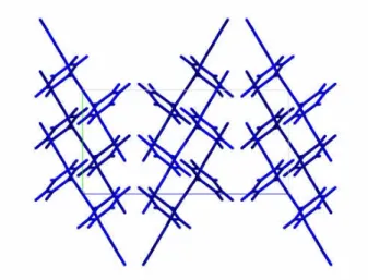
Figure 2.5: A top view of the ab- plane crystal structure of rubrene. The herringbone configuration is apparent.
Locally, charge transport in conjugated materials is determined by the charge transfer from one neighbouring molecule to another and is therefore very sensitive to orientation of the molecules with respect to each other. The electronic coupling between adjacent molecules, quantified by the transfer integral t, is modulated by the molecular arrangement and directly associated with the electronic mobility 37-39. In the framework of these calculations, the amplitude of the electronic coupling is influenced by the intermolecular separation distance, the molecular overlap, the length of the molecule, and, in the case of herringbone structures, the rotation of molecular planes38, 40-43.Thus transfer integrals between the adjacent molecules in these crystals vary significantly depending on the crystallographic direction39, 41, 44. One apparent implication is that the charge carrier mobility within a molecular plane (ab plane in
Electronic properties of molecular crystals
rubrene) is much more efficient in comparison to charge carrier transport between layers (c direction). This strong anisotropy of transport properties of organic crystals has been well documented in the TOF experiments45. The conductivity anisotropy within the ab-plane is anticipated to be less pronounced. However, prior to the development of single-crystal OFETs, the anisotropy had never been observed in the field-induced transport on the surface of organic semiconductors. Several types of single-crystal OFETs based on rubrene demonstrate anisotropy of surface conductivity 46-48 . In rubrene devices based on PDMS stamps, the mobility along the crystallographic b axis exceeds the mobility along the a axis by a factor of ~ 3 (Figure 2.6). Similar anisotropies have been observed for rubrene transistors with parylene gate dielectrics as well. A clear correlation between the mobility and molecular packing has also been found recently in a family of tetrathiafulvalene derivatives49 and in air-gap transistors built on tetracene crystals50. Recently, non-destructive probing techniques have been developed that allow the exploration of these anisotropies at high angular resolution without having to move the fragile crystals around.51
Figure 2.6: (Left) Molecular packing in the rubrene crystal. Blue arrow indicates the direction of highest mobility (Right) Charge carrier mobility anisotropy on the surface of rubrene crystal46
Electronic properties of molecular crystals
2.3 Charge transport characteristics of organic single crystals
Due to the weak van der Waals bonding between the individual organic molecules, many electronic properties of these organic solids are determined by the property of the molecule itself- specifically the energy gap between the highest occupied and lowest occupied molecular orbitals (HOMO and LUMO). The transport mechanism is usually understood with respect to the limiting cases of small polaron transport and bandlike transport corresponding to the extreme localization or delocalization of the charge carriers.
2.3.1 Band like transport
The classical work performed by N. Karl and coworkers on highly purified naphthalene and perylene single crystals revealed the first proof of band transport in organic molecular crystals52-54.Mobilities as high as 400 cm2/Vs were obtained at 10K and 3kV/cm by the time-of –flight method (Figure 2.7) in extremely pure naphthalene crystals. These TOF velocities could not be explained by charge hopping models.
Electronic properties of molecular crystals
Figure 2.7: Electron and hole mobilities in the a-direction of highly purified naphthalene crystals for different field strengths. Adapted from 53
In addition, the sub-linear velocity-field relation at high fields observed in these samples could be explained by the Schottky model of acoustic deformation potential scattering by hot charge carriers, a model which is based on band transport.Thus the authors53 proposed that the charge carrier transport in pure and perfect low molecular weight aromatic organic photoconductor crystals at low temperature can be described by coherent transport in bands. Space charge limited current measurements on ultrapure pentacene 55 as well as in tetracene 56 single crystals have shown intrinsic band like transport. Picosecond transient photoconductivity measurements conducted on a variety of organic crystals including rubrene support the band picture as well 57-59.
It is conceivable that in organic crystals where the molecules are in an ordered arrangement, each molecular π system can interact with the π systems of the adjacent
Electronic properties of molecular crystals
molecules resulting in the formation of energy bands in the crystal. The crystal valence bands originate from the overlapping HOMO’s of the individual molecules, whereas the conduction band is formed by the overlapping of the LUMOs. The organic semiconductors are normally characterized by wide bandgaps and small bandwidths. The molecular crystal’s bandwidth is related to the orbital overlap strength of the HOMOs and the LUMOs. Calculations have shown that the bandwidths are in the range of 0.1 -0.5 eV 60-62. This compares unfavourably with the values in inorganic semiconductors like silicon (10 eV) and could explain the huge difference in the mobilities.
2.3.2 Influence of traps
Since organic crystals possess a better crystalline order and reduced concentration of defects, they are expected to have a very low concentration of electrical traps. The reduced number of defects still creates localized electrical states in the HOMO-LUMO gap. The impact of these traps on the electrical transport properties depends on their location in the energy gap. In the case of p-type carriers, if the traps exist near the edge of HOMO, separated by energy of a few kBT, they act as shallow traps. If the energy of the localized state is separated from the mobility edge by more than a few kBT, they are characterized as deep traps. Once a charge is trapped in a deep state, it cannot be released by thermal energy alone. For the pristine surface of rubrene single crystals at room temperature, for instance, the density of deep traps can be as low as 1010 cm–2.Shallow traps on the other hand are characterized by a finite trapping time. After being trapped for a characteristic time τtr, a polaron can be thermally activated and released to the band. The effect of shallow traps on charge transport is normally described in terms of the multiple trap and release (MTR)63, 64 model. According to this model, not all the charges induced in the transistor on application of a voltage VG above the threshold voltage Vth contributes to the current. A fraction of the mobile charge can be momentarily trapped by shallow traps-the fraction being determined by
Electronic properties of molecular crystals
the number of traps and the temperature (which determines the τtr). This idea can be represented in two ways- either by assuming that all the carriers induced above the threshold flow, but with a lower effective mobility than the intrinsic mobility or by assuming that the number of carriers moving at any time is limited, but they travel at the intrinsic trap free mobility. The first approach can be described by:
)
(
)
(
)
(
)
(
0T
T
T
T
tr effτ
τ
τ
µ
µ
+
=
Here τtr(T) is the average trapping time on shallow traps while τ(T) is the average time that a polaron spends diffusively travelling between the consecutive trapping events. Thus the intrinsic mobility is only realised when the τ is much more than τtr which happens when there is a low concentration of defects or when the temperature is high enough to ensure rapid detrapping. This regime allows the exploration of the intrinsic properties of the crystal surface like mobility anisotropy.
Electronic properties of molecular crystals
Figure 2.8: Temperature dependent conductivity measurements on the rubrene transistor showing the trap limited regime at low temperatures and intrinsic regime at higher temperatures
Figure 2.8 reveals the two regimes at play in the temperature dependent characteristics of rubrene single crystal transistors. At higher temperatures (above 150K), the intrinsic properties like the pronounced anisotropy difference for conductivity along the b-axis and the a-axis. As the temperature is lowered, the charges localized in the shallow traps are released after a much longer timescale. This is indicated by the rapid fall in mobility values below 150K where the traps dominate. This transition temperature would be strongly dependent on the concentration of the traps with a higher concentration shifting this threshold to a higher temperature. The classical work performed by N.Karl and co-workers on ultrapure crystals of naphthalene and perylene revealed similar results with an increase in the mobility (up to 400 cm2/Vs)
Electronic properties of molecular crystals
with the lowering of temperature (intrinsic regime) until the shallow traps become active and result in a reduction of the effective mobility.47, 53
The high-quality TOF data of Karl et al implies that coherent transport characterizes the intrinsic charge transport in ultra-pure organic single crystals. However the calculation of the charge carrier’s mean free path from experimental evidence indicates that they are smaller than the intermolecular distance62. This of course violates the assumption of charge delocalization necessary for the band model. In narrow-band molecular solids, polarization effects favor localization of charge carriers and narrow the bandwidth even further. This results in self-trapped electronic states called polarons which differ in their behavior from nearly free electrons (necessary for band-type behavior) and strongly localized electrons (which can lead to hopping behavior). The next section discusses polaron formation and transport
2.3.3 Polaron transport
Polarons are quasiparticles composed of a charge carrier accompanying its polarization field. The polarization field causes a distortion in the local lattice. As the charge moves through the crystal, the electron carries the lattice distortion with it. The resulting lattice polarization acts as a potential well that hinders the movements of the charge, thus decreasing the mobility. In an organic molecular crystal, the polarization associated with the charge include the polarization of the electronic orbitals on molecules surrounding the excess charge which is caused due to the interaction of the charge with the induced dipole moments and quadrupole moments of the surrounding molecules.
The term of polaron owes its origin to that it was considered for the case of polar crystals, where interactions between electrons and optical polarizations are
Electronic properties of molecular crystals
particularly strong, so that an excess carrier creates a local distortion of the lattice in which it is self-trapped. The indications for polaron-formation in organic molecular crystals can be seen in photo-emission experiments.62 Photoemission data from single crystals generally show lines that are broadened and shifted in energy relative to the corresponding gas phase spectral lines. The broadening is suggested to originate from fluctuations in the intermolecular electronic polarization while the spectral line shift can be explained by the increased binding energy of a charge due to polarizations in the local crystal environment. Pioneering theoretical work in this area was done by Holstein65, who introduced the concept of small-polaron bands for a local (on-site) electron –phonon coupling. A small polaron is one whose linear dimensions are of the order of one lattice spacing. The main prediction of his theory is that the mobilities initially decrease with rising temperature T due to bandwidth narrowing but increase again for higher T due to phonon-assisted hopping.
Interestingly electron mobility values of naphthalene single crystals below 100K follows a power law (proportional to T-1.5) consistent with the band model. However, between 100K and 300K the electron mobility along the crystallographic c direction remains constant 45. This constant region has been described as the superposition of two independent carrier mechanisms. According to Silinsh et al66 the first mechanism is described using the concept of an adiabatic, nearly small molecular polaron (MP),in which the carriers are treated as heavy polaron-type quasiparticles, which are formed as a result of the interaction of the carriers with intramolecular vibrations of the local lattice environment, and move coherently via tunneling. The second mechanism involves a small lattice polaron (LP), which moves by thermally activated hopping and thus exhibits a typical exponential dependence of mobility on temperature. This polaronic hopping-type temperature dependence has also been measured for the electron mobility in pyrene and for the hole mobility in perylene45. Kenkre et al67 were also able to fit the measured electron mobilities reasonably well to Holstein’s model assuming directionally dependent local-coupling constants.
Electronic properties of molecular crystals
Despite the success of such fitting procedures, there was a need for a first-principles description of charge-carrier mobilities in organic crystals that could explain the different behavior of electrons and holes, the microscopic origin of the crystallographic anisotropy in the temperature dependence and the influence of nonlocal (Peierls-type) couplings. This has been compensated by the proposal of a Holstein-Peierls model by Hannewald et al68, 69 which is based on Holstein’s original concept of small-polaron bands but generalized with respect to the inclusion of nonlocal electron-phonon coupling. Using this model and microscopic parameters derived from ab-initio calculations, the authors were able to reproduce the experimental data in naphthalene69. The model, however, only accounts for the intermolecular optical modes and neglects the contribution from intra-molecular vibrations and the coupling to acoustic modes that play a significant role in charge transport.70
The polaron theories described above are mostly applicable to charge conduction in the bulk of the crystal for a low density of charge carriers (as is the case in TOF experiments). On the surface of rubrene single crystal transistors where the density of charge carriers is much higher due to its proximity to a polar dielectric, conduction has been proposed to occur through the motion of Fröhlich polarons71 In common inorganic semiconductors, the effective strength of the interactions that create Fröhlich polarons are weak due to both the low ionic polarizabilities and the low band masses of these materials. This is not the case in organic transistors where the band masses are high due to the weak van der Waals bonding while using gate dielectrics with increasing ionic polarizabilities permits the strength of interaction to be tuned from weak to the strong coupling regimes.
Electronic properties of molecular crystals
Figure 2.9: Temperature dependence of the carrier mobility for six different gate dielectrics. The temperature dependence evolves from metallic-like to insulator-like, as the dielectric constant is increased.
The gate modulated electrostatic ‘doping’ of charge carriers in organic single crystal transistors allows the observation and study of new phenomena. For example, the use of highly polarizable Ta2O5 gate dielectrics allows a high carrier density regime (0.1 carrier per molecule) which enables observation of coulombic repulsion in the Fröhlich polarons and drain current saturation in transistors.72
Recently, Troisi 73et al have proposed in a recent computational paper that, at room temperature, the transfer integral between close molecules is strongly modulated by thermal motions. Since the amplitude of this modulation is of the same order of magnitude as the average transfer integral, the translational symmetry of the electronic Hamiltonian is completely lost and the overall electronic structure of the crystal resembles that of an amorphous material. The sensitivity of the transfer integral to small nuclear displacements (discussed previously in this chapter) was recognized by these authors as the crucial difference between transport mechanisms in
Electronic properties of molecular crystals
organic and inorganic semiconductors. A minimalist model Hamiltonian37 that neglects the effect of reorganization energy and considers only the fluctuation of the transfer integral has been used to explain the temperature dependence of the charge mobility of organic semiconductors and has been applied to predict the absolute charge mobility of rubrene.74
In conclusion, this chapter has discussed the basic theory of charge transport in organic crystals including the origin of semiconducting behaviour in organic molecules. The intermolecular interactions that shape the order and arrangement of organic molecules in lattices have been described. The position and orientation of the molecules modulate the intermolecular transfer integral which determines the charge transfer properties of these molecules. The band model which is commonly used to discuss the charge transport in single crystals was also introduced here along with the characteristics of polaron transport in these materials. The widespread interest in unraveling the underlying factors determining the charge transport is spurring the development of new theories which consider local and non-local interactions between the charge carrier and its environment.
Electronic properties of molecular crystals 2.4 References
1. A. Assadi, C. Svensson, M. Willander and O. Ingana?s, Applied Physics
Letters, 1988, 53, 195-197.
2. Z. Bao, A. Dodabalapur and A. J. Lovinger, Applied Physics Letters, 1996, 69, 4108-4110.
3. R. J. Kline, M. D. McGehee, E. N. Kadnikova, J. Liu, J. M. J. Fre?chet and M. F. Toney, Macromolecules, 2005, 38, 3312-3319.
4. J. Paloheimo, H. Stubb, P. Yli-Lahti and P. Kuivalainen, Synthetic Metals, 1991, 41, 563-566.
5. A. Tsumura, H. Koezuka and T. Ando, Applied Physics Letters, 1986, 49, 1210-1212.
6. B. S. Ong, Y. Wu, P. Liu and S. Gardner, Journal of the American Chemical
Society, 2004, 126, 3378-3379.
7. E. Lim, Y. M. I. Kim, J. I. K. Lee, B. J. Jung, N. S. Cho, J. Lee, D. O. Lee-Mi and H. K. Shim, Journal of Polymer Science, Part A: Polymer Chemistry, 2006, 44, 4709-4721.
8. H. Sirringhaus, R. J. Wilson, R. H. Friend, M. Inbasekaran, W. Wu, E. P. Woo, M. Grell and D. D. C. Bradley, Applied Physics Letters, 2000, 77, 406-408. 9. J. G. Laquindanum, H. E. Katz, A. J. Lovinger and A. Dodabalapur, Chemistry
of Materials, 1996, 8, 2542-2544.
10. Y. Y. Lin, D. J. Gundlach and T. N. Jackson, Annual Device Research Conference Digest, 1996.
11. Y. Y. Lin, D. J. Gundlach, S. F. Nelson and T. N. Jackson, IEEE Electron
Device Letters, 1997, 18, 606-608.
12. H. Moon, R. Zeis, E. J. Borkent, C. Besnard, A. J. Lovinger, T. Siegrist, C. Kloc and Z. Bao, Journal of the American Chemical Society, 2004, 126, 15322-15323.
13. M. L. Tang, A. D. Reichardt, N. Miyaki, R. M. Stoltenberg and Z. Bao,
Journal of the American Chemical Society, 2008, 130, 6064-6065.
14. C. D. Dimitrakopoulos, A. R. Brown and A. Pomp, Journal of Applied Physics, 1996, 80, 2501-2508.
15. C. D. Dimitrakopoulos, S. Purushothaman, J. Kymissis, A. Callegari and J. M. Shaw, Science, 1999, 283, 822-824.
Electronic properties of molecular crystals
16. H. Klauk, M. Halik, U. Zschieschang, G. Schmid, W. Radlik and W. Weber,
Journal of Applied Physics, 2002, 92, 5259.
17. S. F. Nelson, Y. Y. Lin, D. J. Gundlach and T. N. Jackson, Applied Physics
Letters, 1998, 72, 1854-1856.
18. F. Garnier, G. Horowitz and D. Fichou, Synthetic Metals, 1989, 28, 705-714. 19. F. Garnier, G. Horowitz, D. Fichou and A. Yassar, Synthetic Metals, 1996, 81,
163-171.
20. F. Garnier, G. Horowitz, X. Peng and D. Fichou, Advanced Materials, 1990, 2, 592-594.
21. F. Garnier, G. Horowitz, X. Z. Peng and D. Fichou, Synthetic Metals, 1991, 45, 163-171.
22. G. Horowitz, D. Fichou, X. Peng, Z. Xu and F. Garnier, Solid State
Communications, 1989, 72, 381-384.
23. J. March, Advanced Organic Chemistry, John Wiley & Sons, New York, 1985. 24. M. Knupfer, J. Fink, E. Zojer, G. Leising and D. Fichou, Chemical Physics
Letters, 2000, 318, 585-589.
25. C. C. Mattheus, A. B. Dros, J. Baas, A. Meetsma, J. L. De Boer and T. T. M. Palstra, Acta Crystallographica Section C: Crystal Structure Communications, 2001, 57, 939-941.
26. C. C. Mattheus, G. A. De Wijs, R. A. De Groot and T. T. M. Palstra, Journal
of the American Chemical Society, 2003, 125, 6323-6330.
27. C. C. Mattheus, A. B. Dros, J. Baas, G. T. Oostergetel, A. Meetsma, J. L. De Boer and T. T. M. Palstra, Synthetic Metals, 2003, 138, 475-481.
28. R. C. Haddon, X. Chi, M. E. Itkis, J. E. Anthony, D. L. Eaton, T. Siegrist, C. C. Mattheus and T. T. M. Palstra, Journal of Physical Chemistry B, 2002, 106, 8288-8292.
29. M. D. Curtis, J. Cao and J. W. Kampf, J. Am. Chem. Soc., 2004, 126, 4318-4328.
30. C. A. Hunter and J. K. M. Sanders, Journal of the American Chemical Society, 1990, 112, 5525-5534.
31. G. R. Desiraju and A. Gavezzotti, Journal of the Chemical Society, Chemical
Communications, 1989, 621-623.
Electronic properties of molecular crystals
33. R. B. Campbell, J. M. Robertson and J. Trotter, Acta Crystallogr., 1962, 15, 289-290.
34. O. D. Jurchescu, A. Meetsma and T. T. M. Palstra, Acta Crystallographica
Section B, 2006, 62, 330-334.
35. D. E. Henn, W. G. Williams and D. J. Gibbons, Journal of Applied
Crystallography, 1971, 4, 256.
36. J. E. Anthony, D. L. Eaton and S. R. Parkin, Organic Letters, 2002, 4, 15-18. 37. A. Troisi and G. Orlandi, Physical Review Letters, 2006, 96, 086601-086604. 38. J. Cornil, D. Beljonne, J. P. Calbert and J. L. Bre?das, Advanced Materials,
2001, 13, 1053-1067.
39. Y. C. Cheng, R. J. Silbey, D. A. Da Silva Filho, J. P. Calbert, J. Cornil and J. L. Bre'das, Journal of Chemical Physics, 2003, 118, 3764.
40. J. L. Bre'das, D. Beljonne, V. Coropceanu and J. Cornil, Chemical Reviews, 2004, 104, 4971-5003.
41. J. L. Bre'das, J. P. Calbert, D. A. Da Silva Filho and J. Cornil, Proceedings of
the National Academy of Sciences of the United States of America, 2002, 99,
5804-5809.
42. O. Kwon, V. Coropceanu, N. E. Gruhn, J. C. Durivage, J. G. Laquindanum, H. E. Katz, J. Cornil and J. L. Bre?das, Journal of Chemical Physics, 2004, 120, 8186-8194.
43. V. Lemaur, D. A. Da Silva Filho, V. Coropceanu, M. Lehmann, Y. Geerts, J. Piris, M. G. Debije, A. M. Van De Craats, K. Senthilkumar, L. D. A. Siebbeles, J. M. Warman, J. L. Bre?das and J. Cornil, Journal of the American Chemical
Society, 2004, 126, 3271-3279.
44. G. A. De Wijs, C. C. Mattheus, R. A. De Groot and T. T. M. Palstra, Synthetic
Metals, 2003, 139, 109.
45. N. Karl, in Organic electronic materials, eds. R. Farchioni and G. Grosso, Springer-Verlag, Berlin, Editon edn., 2001.
46. V. C. Sundar, J. Zaumseil, V. Podzorov, E. Menard, R. L. Willett, T. Someya, M. E. Gershenson and J. A. Rogers, Science, 2004, 303, 1644.
47. V. Podzorov, E. Menard, A. Borissov, V. Kiryukhin, J. A. Rogers and M. E. Gershenson, Physical Review Letters, 2004, 93, 086602.
48. R. Zeis, C. Besnard, T. Siegrist, C. Schlockermann, X. Chi and C. Kloc,