HAL Id: tel-00681846
https://tel.archives-ouvertes.fr/tel-00681846
Submitted on 22 Mar 2012HAL is a multi-disciplinary open access archive for the deposit and dissemination of sci-entific research documents, whether they are pub-lished or not. The documents may come from teaching and research institutions in France or abroad, or from public or private research centers.
L’archive ouverte pluridisciplinaire HAL, est destinée au dépôt et à la diffusion de documents scientifiques de niveau recherche, publiés ou non, émanant des établissements d’enseignement et de recherche français ou étrangers, des laboratoires publics ou privés.
Les fils photoniques : une géométrie innovante pour la
réalisation de sources de lumière quantique brillantes
Nitin Singh Malik
To cite this version:
Nitin Singh Malik. Les fils photoniques : une géométrie innovante pour la réalisation de sources de lumière quantique brillantes. Physique [physics]. Université de Grenoble, 2011. Français. �NNT : 2011GRENY069�. �tel-00681846�
THÈSE
Pour obtenir le grade de
DOCTEUR DE L’UNIVERSITÉ DE GRENOBLE
Spécialité : PHYSIQUE/ PHYSIQUE DE MATIERE CONDENSE & RAYONNEMENTArrêté ministériel : 7 août 2006
Présentée par
Nitin Singh MALIK
Thèse dirigée par Jean-Michel GERARD et co-encadrée par Julien CLAUDON
préparée au sein de l’équipe mixte CEA-CNRS « NanoPhysique et SemiConducteurs », Service de Physique des Matériaux et Microstructures, INAC, CEA Grenoble
dans l'École Doctorale de Physique de Grenoble
Les
fils
photoniques :
une
géométrie innovante pour la
réalisation
de
sources
de
lumière quantique brillantes
Thèse soutenue publiquement le 21 novembre 2011,devant le jury composé de :
Laurent SAMINADAYAR
Professeur Université Joseph Fourier (Président)
Isabelle SAGNES
Directeur de Recherche CNRS (Rapporteur)
Guillaume CASSABOIS
Professeur Université Montpellier 2 (Rapporteur)
Christian SEASSAL
Directeur de Recherche CNRS (Examinateur)
Jean-Michel GERARD
Eq. Directeur de Recherche, CEA Grenoble (Directeur)
Julien CLAUDON
Acknowledgements
At the time of writing my dissertation, I am feeling just like walking this journey through time again. That was the last week of February but around three years ago when I was applied for this position in Joint Group of CEA-CNRS, NPSC ‹‹ Nanophysique et Semiconducteurs ›› Grenoble FRANCE, indeed almost half a world away from my home country. In the last week of September in that year, I started my research work in the Group NPSC you will see here is this dissertation. At NPSC, I have been fortunate enough to be surrounded by many kind people to offer help and useful guidance to complete my research there, so first I owe a debt of deep gratitude to the many people who contributed to my maturity as researcher and analytical thinker at NPSC.
First and foremost, I would like to express my deepest gratitude and indebtedness to my Director of thesis Jean-Michel Gérard and my Supervisor Julien Claudon, who offered me this opportunity to work in this group and guided me throughout my research. In spite of his busy schedule, Jean-Michel always made time for individual meetings to discuss about the progress and problem of projects and always gave his invaluable guidance and suggestions.
I would also like to thank Prof. Henri Mariette, Director of the group NPSC, to give opportunity me to work in this group and support me throughout my dissertation.
Again a special thank goes to my supervisor Julien Claudon, a truly incredible research advisor and mentor and above all a nice human being, for the great support and invaluable guidance he has provided me throughout my dissertation. I would say that never once did he act like my boss nor did he ever treat me like a PhD student. Although we worked together most of the time of my dissertation but he never looked over my shoulder to make sure I was working properly or not, yet he was always one door away whenever I needed him for advice (some time for coffee too !). He is role model for me. He expertly guided me to success in many projects I worked on, and I have benefited from his intelligence, critical thinking, creativity and rigorous approach to science. I also thank him for his generous support in other aspects, particularly when I had some health problem. It was his really great effort that gave me courage to think positive and to finish my work in such conditions.
I would also like to convey many many thanks to the members of the jury: Guillaume Cassasbois, Isabelle Sagnes, Laurent Saminadayar and Christian Seassal for refereeing my thesis and accepting to serve in the jury. Their
valuable and constructive comments helped me to improve manuscript to its present shape.
If I ever felt honored to be dependent on the work of so many co-workers involved in growth and optical characterization of the devices, it is because of my colleagues Emmanuel Dupuy, Joël Bleuse, Maela Bazin, Matheiu Munsch, Megan Creasey and Périne Jaffernnou. My thanks also go to other fellows in the NPSC who have been a help: Catherine, Edith, Eva, Gabriel, Herve, Jean, Jean-Phillipe, Joël Eymery, Kuntheak, Lionel, Marléne, Régis, Rudeesan, Vincent, Yann and Yoann. It was a real pleasure to work in such an open, healthy and collaborative environment.
I would also like to acknowledge financial support from the Nanosciences fondation. I would like to thank the technical team of PTA clean room to help me during my research.
A special thanks to Carmelo and Cecile, for their great help dealing with travel and administration matters efficiently during my dissertation.
To Prof. Sujeet Chaudhary, I will never be able to thank you enough for allowing me to work in your lab at IIT Delhi when I was in my M.Tech. You have been the mentor of my improvement from a below average student of science to a graduate research student. The opportunity you provided me and the value of the experience and your support that I received is difficult to put into words, nonetheless, thank you for everything. Huge thanks goes to Prof. Inderjeet Singh, the one who taught physics to me in a wonderful way and motivated me to do research in physics.
I cannot imagine my years at NPSC without two friends, Prem and Sandeep. They are wonderful friends, and they have painted a rich fabric of memories that I will never forget. I have shared an office with Sandeep for two years of my thesis. Because of his presence I never felt I am far from my country. I want to give a special thanks to Veeresh with whom I shared the apartment. A lot of people have also been helping me and pushing me forward during all these years of my research, so special thanks to my friends: Abhinav, Agnieszka, Alexander, Alisher, Amit, Aparna, Bijandra, Gajender, Irina, Pankaj, Pawan, Madhav , Manan, Robert, Sanjay, Tapas, Teju, Xiaojun and Yulia.
Before I finish, I would like to express my deepest gratitude to my parents as well as my brother, my sisters. They have always supported me, trusted me and allowed me for the challenge of studying abroad. I have always felt their warm and strong support during my research. How could it be possible for me to go this far without your support, encouragement and patience? I love you all. I
would like also like to thank Priya, who provided the moral support as a best friend and sister so critical in keeping me on track, in both the best and worst phase of my life. Her words (as like a grandmother) of encouragement helped me traveled the journey of my research. I dedicate this dissertation to my late grandfather. I was not able to visit him when he was badly ill, and hope the accomplishment of this dissertation could fulfill his last wish. May he rest in peace.
i
Contents
1. Introduction ... 1
1.1 General introduction and motivation ... 1
1.1.1 On-demand single photon sources ... 1
1.1.2 On-demand single photon emission ... 2
1.2 Semiconductor quantum dots as single-photon emitters ... 4
1.2.1 Growth of self-assembled quantum dots ... 4
1.2.2 A single dot as a single photon emitter ... 5
1.2.3 Improving the collection efficiency ... 9
1.3 Various approaches to control spontaneous emission ... 10
1.3.1 How to control spontaneous emission rates ... 10
1.3.1.1 Influence of the density of photonic states ... 11
1.3.1.2 Controlling the amplitude of the zero-point fluctuations ... 12
1.3.2 Two major strategies to control SE ... 14
1.3.2.1 Resonant SE control: the Purcell effect ... 14
1.3.2.2 Limits of a resonant approach ... 16
1.3.2.3 First examples of SE control in a waveguide ... 17
1.4 This thesis ... 18
1.4.1 Fiber-like photonic nanowires ... 19
1.4.2 Outlines of the thesis ... 20
1.5 Contribution to the experimental work ... 21
References ... 25
2. Design of high efficiency single photon sources based on photonic nanowire ... 31
2.1 Control of spontaneous emission in an infinite photonic nanowire... 32
2.1.1 Coupling to the guided mode ... 33
2.1.1.1 Guided modes supported by a photonic nanowire ... 33
2.1.1.2 Generalized Purcell factor of a guided mode ... 34
2.1.1.3 Generalized Purcell factor of the fundamental guided mode ... 36
2.1.1.4 Link with the decay rate of a quantum dot ... 38
2.1.2 Coupling to the radiative modes and dielectric screening ... 39
2.1.2.1 Some basics of electrostatic in a dielectric material ... 40
2.1.2.2 Screening in a thin dielectric cylinder ... 41
2.1.2.3 Dielectric screening in other geometries ... 44
2.1.2.4 Dielectric screening in a thick cylinder ... 45
ii
2.1.3.1 On-axis emitter case ... 46
2.1.3.2 Influence of the spatial position of the emitter ... 48
2.2 Optimization of far-field radiation pattern ... 49
2.2.1 Collection issues ... 49
2.2.2 Fabry-Perot model ... 50
2.2.3 Bottom mirror ... 53
2.2.3.1 Bragg mirror ... 53
2.2.3.2 Metallic mirror ... 56
2.2.4 Tapering of the top facet of the wire ... 57
2.2.4.1 Regular taper ... 57
2.2.4.2 Inverted taper ... 59
2.3 Two possible designs and their performance ... 60
2.4 Conclusion ... 62
References ... 63
3. Fabrication of high efficiency single photon sources in the photonic nanowire geometry ... 64
3.1 Introduction ... 65
3.2 Single photon sources design ... 65
3.3 Fabrication of single photon sources ... 67
3.3.1 Starting point ... 67
3.3.2 Deposition of bottom mirror ... 69
3.3.3 Flip chip process ... 70
3.3.3.1 Wafer bonding ... 70
3.3.3.2 Growth substrate removal ... 72
3.3.3.3 Etching of sacrificial layer ... 74
3.3.4 Fabrication of regular tapered photonic nanowire ... 74
3.3.4.1 Hard mask deposition ... 75
3.3.4.2 Defining an Al mask using Electron beam lithography ... 76
3.3.4.3 Defining the wires with reactive ion etching ... 77
3.3.5 Fabrication of trumpet like photonic nanowire ... 87
3.3.5.1 Deposition of anti-reflection coating ... 88
3.3.5.2 Choice and definition of the etching mask ... 89
3.3.5.3 Reactive ion etching: Pattern transfer process ... 89
3.4 Conclusion ... 94
References ... 94
4. Optical performance of the cylindrical photonic nanowire ... 97
4.1 Control of spontaneous emission of quantum dot by photonic nanowire ... 98
iii
4.1.2 Photoluminescence spectra ... 99
4.1.3 How to investigate SE control in a photonic nanowire ... 100
4.1.4 Dielectric screening and inhibition of SE into radiative modes ... 102
4.1.5 Coupling to the guided mode and enhancement of SE ... 105
4.1.6 Global picture of SE in photonic nanowires ... 106
4.1.7 Measuring the quantum efficiency of the emitter with photonic wire ... 107
4.1.8 Discussion of SE control ... 108
4.2 On-demand single-photon emission from a QD inserted in a photonic nanowire ... 109
4.2.1 Micro-photoluminescence spectrum ... 109
4.2.2 Photon statistics of single photon source ... 111
4.2.2.1 A few words about photon statistics ... 111
4.2.2.2 Experimental setup (HBT) ... 114
4.2.3 Purity of single photon emission ... 115
4.2.4 Efficiency of the single photon source ... 116
4.2.4.1 Determination of the efficiency using Ti:Sa laser ... 117
4.2.4.2 Validation of calibration method ... 118
4.2.4.3 Efficiency of the photonic wire ... 119
4.2.5 Discussion ... 120
4.2.5.1 Some practical considerations ... 120
4.2.5.2 Purity of single-photon emission ... 120
4.2.5.3 Source Efficiency ... 122
4.3 Conclusion ... 122
References ... 122
5. Control of photon polarization by elliptical photonic nanowire ... 125
5.1 Single-mode emission : motivation and state-of-art ... 126
5.1.1 Context and motivations ... 126
5.1.2 State-of-the-art: cavity based devices ... 126
5.2 Control of photon polarization with photonic wire ... 128
5.2.1 The case of circular photonic nanowire ... 128
5.2.2 Spontaneous emission control in elliptical photonic nanowires ... 129
5.2.2.1 Selective deconfinement of one mode ... 129
5.2.2.2 Generalized Purcell factor associaled with the guided modes ... 130
5.2.3 SE control and -factor ... 131
5.3 Low energy excitonic complexes trapped in a QD ... 133
5.4 Fabrication of elliptical photonic nanowires ... 135
5.4.1 MBE sample ... 135
iv 5.5 Experimental results ... 140 5.5.1 Optical setup ... 140 5.5.2 Polarization analysis ... 141 5.5.3 A complementary measurement ... 143 5.6 Conclusion ... 145 References ... 145
6. Conclusion and perspectives ... 147
6.1 Conclusion ... 147
6.2 Perspectives ... 149
1
Chapter-1
Introduction
1.1 General Introduction and Motivation
1.1.1 On-demand single photon sources
Ideally, an on-demand single-photon source is a device, able to emit a light pulse containing exactly one photon in an optical channel of interest after a trigger pulse (electrical or optical) ( see Figure 1.1). Such a device would enable many applications in the field of quantum information technology [1,-8]. The first important one is quantum key distribution, which provides a way for unconditional secure optical communication between two parties [5, 6]. A possible application to linear optical quantum computing arises, providing that the source emits indistinguishable photons [7]. This demanding criterion imposes that the photons are emitted in the same quantum states (well defined frequency, temporal profile, same spatial mode and polarization). In that case, photon interferences can be exploited to implement quantum algorithms. This is however very demanding and makes this goal a long term objective. A single-photon source, emitting a faint light flux with a low photon noise (zero for an ideal source), might also find applications in metrology [3]. In that case, indistinguishability is not required.
2 For all these applications, we have at least two key figures of merit:
- The purity of single-photon emission: the emitted light pulses should contain
exactly one photon (and not more). A deviation from this ideal case is captured by the second order intensity correlation function g2 (further details will be given in Chapter 4).
- The efficiency of the source: In this thesis, we will consider emission into
free-space: the optical channel of interest is the collecting cone of the first lens of the optical setup (a microscope objective). The efficiency of the source is then defined as the probability to collect a photon in the microscope objective after a trigger pulse. With this definition, the efficiency is independent on the setup transmission losses and the quantum efficiency of the detectors.
In this thesis, we will show how to realize a bright single-photon source using a solid-state single-photon emitter (a semiconductor quantum dot) inserted in a photonic structure optimised to achieve high collection efficiency. Our strategy is in fact a two step one. The quantum dot is integrated in a photonic structure providing a well controlled electromagnetic environment, to funnel a large fraction of its spontaneous emission into an optical mode of interest. In a second step, the collection of the photon is optimized through a specific photonic engineering. In this chapter, we present quantum dots and the various approaches to control their spontaneous emission, with a special emphasis on the realization of semiconductor single-photon sources.
1.1.2 On-demand single photon emission
In the last decade, considerable efforts have been made to develop single-photon sources [9], and a distinction can be established between approximate and „true‟ single photon sources.
Approximate single-photon sources
The easiest and most straightforward way to produce a regulated single-photon stream is to attenuate a pulsed laser [10]. This approach has been used to implement quantum cryptography schemes [11, 12]. Well above the lasing threshold, the photons emitted by the laser follow a Poissonian statistics (they are emitted independently from each other). This statistics is preserved when the laser beam is attenuated using neutral filters.
Let us consider a strongly attenuated beam, for which the average photon number per pulse is smaller than unity. In that case, if the probability to emit one photon is p (1), the probability to emit two photon is p(2) = p(1)²/2, which is
3 shown in Figure 1.2. This gives rise to a potentially important security leakage known as photon number splitting attack [15]. To avoid multi-photon pulses, p(1) has to be made very small (below 10%), leading to a degraded source efficiency. Thus, there is always a trade off between the efficiency and the purity of the single-photon emission.
Alternatively, photon pairs can be obtained by spontaneous parametric down conversion, using a laser beam impinging on a non linear crystal [13, 14]. In that case, a „signal‟ and „idler‟ photons are emitted simultaneously. One of the photon (e.g. the idler) can be used as a „marker‟ of the emission of the other. However, the emission statistics of the pairs is still Poissonian, putting the same limit on the source efficiency.
Figure 1.2: Photon stream in case of single photon source based on attenuated
laser approach.
‘True’ single photon source: Solid-state quantum emitters
A quantum emitter (like an atom) provides a model system for single-photon emission. Indeed, a two-level fermionic system can only emit a single photon after excitation (because of the Pauli Exclusion Principle). If the excitation is continuous, photons are emitted one by one (antibunched light) when one considers timescales typically shorter than the mean radiative decay of the emitter. The first experiments demonstrating single-photon emission were conducted on atoms; in 1977, Kimble et al. demonstrated light antibunching of the resonance fluorescence from sodium atoms [16]. Since then, other experiments have been carried out on atoms [17], single ion [18, 19]. Because they are considered as more practical, solid-state single-photon emitters have attracted a lot of interest. These present a discrete energy spectrum, with the advantage to occupy a fixed location in space, since they are embedded inside a solid-state matrix. One can cite molecules [20, 21], colour centres in diamond
4 [22-24], semiconductor nanocrystals [25] and other semiconductor quantum dots [26-31].
Among these, semiconductor self-assembled quantum dots feature several appealing properties. A semiconductor quantum dot (QD) is a nanometer sized cluster, which typically contains 104-105 atoms of a semiconductor material, embedded in a matrix of another semiconductor material with a larger band gap [32, 33]. Inside such a QD, the charge carriers (electrons and holes) are confined in the three directions of space, leading to quantized energy levels. As a result, a few discrete bound energy eigenstates with limited degeneracy are available for occupation by carriers. Therefore semiconductor quantum dots (QDs) possess optical properties similar to the one of atoms and are thus often referred to as “artificial atoms”. Moreover, they are photostable neither bleaching nor blinking, feature spectrally-narrow optical emission at cryogenic temperature and present high oscillator strength. In addition, they can be embedded in photonic structures (microcavities and waveguides), and can be excited electrically, using doped and contacted structures. The following section presents their properties with more details.
1.2 Semiconductor quantum dots as single-photon
emitters
In this thesis, we use self-assembled InAs/GaAs quantum dots as single-photon emitters. They have demonstrated excellent single-single-photon emission [29, 30]; therefore we focus on the properties of this system in the following.
1.2.1 Growth of self-assembled quantum dots
We focus on InAs/GaAs quantum dots that are grown by molecular beam epitaxy, using a strain-induced self-assembly method (“Stranski-Krastanov” growth mode). The InAs crystal has a lattice parameter 7% larger than the one of GaAs. For the first monolayer of deposited InAs, the growth mode is 2D and coherent with the GaAs substrate. When the thickness of the InAs layer is further increased, a transition occurs (~1.5 -2.0 ML which depends upon the growth conditions). The strain accumulated in the InAs layer is elastically relaxed through the generation of 3D InAs islands. In order to make them optically active, the dots are finally capped with a GaAs layer. The resulting quantum dots “live” on the top of thin 2D InAs layer which is known as the “wetting layer”. The self-assembly leads to a „double‟ randomness: the nucleation position of the dots is
5 random, and they feature a size distribution, leading to a certain spectral distribution linked to the different confinement energies. Figure 1.3 (a) shows an Atomic Force Microscopic (AFM) image of quantum dots grown under optimized conditions and clearly shows the random nature of the growth of quantum dots. Figure 1.3 (b) shows a transmission electron microscopy (TEM) image of caped QDs which shows the formation of three dimension confinement structures. The surface density of the dots, as well as the average size of the dot can be controlled to some extent by the growth parameters (temperature, growth rate, growth interruptions, etc…).
Figure 1.3: Quantum dot formation: a) AFM image of the uncapped QDs, (b)
TEM image of the cross section of QD structures.
1.2.2 A single quantum dot as a single photon emitter
Discrete energy spectrum:
A schematic of the different energy states of a quantum dot along the growth direction is shown in the Figure 1.4. This figure illustrates that the three dimension confinement in a quantum dot which gives rise to the discrete energy states as like the atom. It shows the first single-particle confined levels: s (no orbital degeneracy) and p (double orbital degeneracy) in the conduction and valence bands. The wetting layer, which is a 2D well with some thickness fluctuation, introduces a continuum of electronic states with a blurred cut-off (corresponding states shown in grey color).
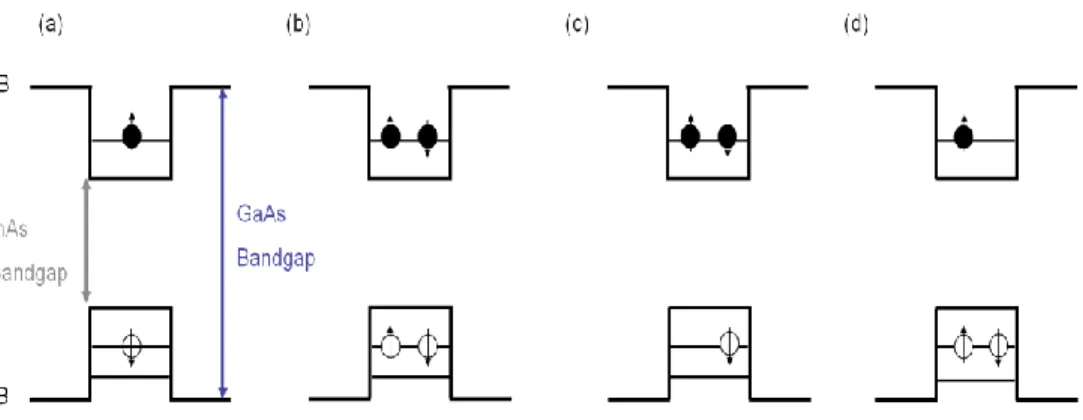
Some excitonic complexes confined in a QD:
A dot can capture electrons and holes. An electron-hole pair trapped in the QD, usually called exciton, can recombine radiatively. In general any number of
6 charges can be trapped inside the QD leading to various confined excitonic complexes. Figure 1.5 shows a number of possible excitonic states of a single quantum dot.
Figure 1.4: Density of states associated with an InAs QD supported by a wetting
layer (QD diameter = 20 nm, height = 1.5 nm, mean thickness of the wetting layer=1.7 ML) [34]
Figure 1.5: Schematic band diagrams of a single quantum dot possible exciton
states; (a) exciton (X1), (b) biexciton (X2), (c) negatively charge exciton (X1-), (d)
positively charge exciton (X1+).
Radiative cascade and on-demand single-photon emission:
We consider here an excitation by a short laser pulse (shorter than the radiative dynamics of the system). This pulse is tuned on an energy exceeding the GaAs bandgap: it thus excites electrons into conduction band, leaving holes in the valence band [29, 30]. These charge carriers are captured by the 2D wetting layer very rapidly (a few ps) before being captured in the excited states of
7 a quantum dot. They then relax via the emission of LO phonons to the lowest unoccupied states of the quantum dots within a few 10 ps [35]. At this stage, the only decay channel is an interband recombination of electrons and holes through the emission of photons [36]. To achieve the brightest single-photon emission, it is desirable to pump efficiently the dot that is to say to inject at least one exciton in the QD per excitation pulse. In first approximation, exciton trapping in the QD can be supposed to be Poisonnian due to the randomness of pumping and capture events. In that case the probability to trap two or more excitons is not negligible. Fortunately, this is not a limitation to use the dot as single-photon emitter, providing a proper spectral filtering is conducted. As shown the in Figure 1.6, when a QD is occupied with more than one electron-hole pairs, the combination of spatial confinement and Coulomb interaction (direct and exchange terms) leads to spectrally different emission energies for each excitonic complex (i.e. X1 X2 X3) [26, 37]. During the progressive
recombination of these, single photons with different energies are thus emitted. In particular, the fundamental transition, corresponding to the recombination of a single exciton (X1) can be isolated by spectral filtering to generate single photons
[27]. Since carriers can be also injected in the GaAs barrier with electrodes and a properly doped structure, this excitation scheme has been readily applied to the realization of single-photon LED [31]. This non-resonant excitation scheme is also thus much more convenient than the resonant electrical excitation presented in Ref. [38].
Figure 1.6: Schematic diagrams of radiative cascade of a single quantum dot
and possible exciton states in case of non-resonant excitation approach. Dark black circles and white circles represent the electrons and holes respectively.
8
Feasibility of the above-mentioned procedure
To collect single-photon emission from a QD, the most critical point is to separate spectrally the exciton (X) from the biexciton (XX) emission. The full width at half maximum (FWHM) of the associated transitions should be smaller than the X-XX spectral separation, on the order of 1-2 meV in InGaAs QDs. This condition is easily meet at cryogenic temperature, where the excitonic line typically displays a FWHM of a few 10 µeV (or below) under non-resonant excitation [39]. When the temperature increases, dephasing processes associated with the coupling to the bulk matrix (in particular acoustic phonons) broaden the lines and set a maximum operation temperature [40, 41]. In addition, for a temperature range 50-100K or higher (for InAs QDs), the onset of thermally activated non-radiative processes spoil the radiative yield of the emitter.
Figure 1.7: Micro-photoluminescence spectrum of a single quantum dot.
Figure 1.7 shows the high resolution µ-PL spectra of a single quantum dot that show a narrow emission line with FWHM~ 70µeV. Ideally it must show the narrow peak as like the delta function of electronic density of states. This deviation comes from homogenous broadening. The homogenous level broadening is an intrinsic QD property since it is result of carrier lifetime, carrier-phonon [42] and carrier-carrier interaction [43].
9
1.2.3 Improving the collection efficiency
A quantum dot is much smaller than the wavelength of the emitted light. Roughly, it thus emits light in all the directions. Moreover, it is embedded in a high index matrix: due to a total internal reflection at the semiconductor-air interface, a very small fraction of the light can be extracted (typically 1%) [45]. To improve the collection efficiency, various solutions have been proposed and developed so far: as discussed below, they can be classified in two categories:
Solutions from geometrical optics:
The first class of solutions is based on geometric optics. A review of several methods can be found in [44, 45]. One can cite mesa supported by a gold mirror, and solid immersion lenses that help to improve the outcoupling efficiency. Experimentally, the obtained efficiencies are in the 10% range [46].
Spontaneous emission control:
Another radically different approach uses a two steps strategy, which is illustrated in Figure 1.8. First, by embedding the emitter into a well chosen photonic structure, we control the spontaneous emission of the emitter, to funnel a large fraction of its SE into an optical mode of interest. Second, the collection of the photons present in the optical mode is optimized, using a specific engineering of the photonic structure.
Figure 1.8: Spontaneous emission control strategy for the efficient single photon
source.
10 M M tot M , (1.1)
with ΓM the SE rate into the target mode, Γtot the total SE rate, equal to ΓM+; is
the SE rate into the continuum of the other modes, named after „radiative‟ or „leaky‟ modes. Achieving a high thus requires ΓM>>, which can be obtained
with an enhancement of ΓM or an inhibition of (or a combination of the two). The
next section presents the physical effects that can be exploited to control the SE rates.
1.3 Various
approaches
to
control
spontaneous
emission
This section presents various tool and approaches to control SE and discusses the associated state-of-the-art. Note also that we will discuss mostly SE control in the context of single-photon sources. It has however a broader interest, e.g. the development of low threshold nano-lasers [47, 48] or the realization of quantum optics experiments with a 1D atom (a two-level) [49].
1.3.1 How to control spontaneous emission rates?
Spontaneous emission is a fundamental process of light-matter interaction by which an emitter undergoes a transition from an excited energy state to a lower energy state and simultaneously emits a photon. Such a process is associated with the zero-point fluctuations of the electromagnetic fields, which destabilizes the excited states of the emitter. For simplicity, we consider here a two level emitter with a fundamental level |g> and an excited state |e>. The energy separation between these levels iseg. This emitter is also supposed to
be point-like, so that we retain only the dipolar term in the interaction with the electromagnetic field. The spontaneous emission rate is given by the Fermi golden rule [28]: ) ( . g e 2 eg 2 2 d.E
,
(1.2)
Here, egis the spectral density of photonic modes seen by the emitter, at the
emitter angular frequency eg; E is the electrical field at the location of the emitter
and d is the dipole operator. It is clear from this expression that depends on the oscillator strength of the atomic transition, but is also highly dependent on the electromagnetic environment of the emitter (through E and eg). In the
11 following, we will briefly summarize the physical effects that offer a control over E and eg
1.3.1.1 Influence of the density of photonic states Dimensionality of the photonic structure:
To achieve single mode emission, a first, natural idea is to use a localized optical mode, confined in a 0D photonic structure (as in microcavity). Ideally, the confinement in the 3 directions of space gives rise to a discrete energy spectrum, associated with resonant modes. However, after a certain time, which is proportional to the quality factor (Q-factor) of the mode, the photons escape from the cavity. Thus, we have to describe a localized mode coupled to a 3D reservoir of optical modes. In the weak coupling regime (characteristic emitter-mode coupling time >> photon escape time), one can show that the cavity mode is described as a quasi-continuum whose spectral density 0D follows a Lorentzian
profile. As pictured in Figure 1.9 (a), its line width at half maximum is inversely proportional to the resonance Q-factor. Because this quasi-continuum describes 1 mode, spectral integration leads to 1. The maximum density of states that can be experienced by a monochromatic emitter is thus proportional to Q.
Figure 1.9: Strategy of SE control of an emitter through the engineering of the
optical density of states by changing the dimension of the surrounding photonic structures.
12 By inserting the emitter inside a waveguide, one can also couple the emitter to a 1D continuum of modes with a spectral density 1D. A typical profile is
shown in Figure 1.9 (b). Such a distribution can also feature peaks, associated with low group velocity vg. In that case, the maximum density of states
experienced by a monochromatic emitter is proportional to the group index „ng=c/vg‟ (c is the speed of light in vacuum). To conclude, in both approaches one
can control the density of photonic modes seen by emitter in comparison to the 3D bulk material (shown in Figure 1.9 (c)) by changing the dimensionality of the photonic structures.
Photonic bandgap structures:
This approach is inspired from the theoretical work of Yablonovitch [47]. In 1987, he invented photonic crystals, in which a periodic structurization of the dielectric function opens a photonic bandgap, that is to say a frequency range for which no optical mode exists. As discussed later on, the motivation was to suppress the SE into the continuum of „useless‟ optical mode. Note that, strictly speaking, a complete photonic bandgap can only exist in an infinite 3D photonic crystal. An excited emitter placed inside a photonic crystal with an emission frequency in this bandgap will not be able to decay radiatively. Inhibition in the optical domain has been demonstrated in 3D- photonic crystal based on Titania inverse opals [50]. It was later realized that strong inhibition of the SE rate of an emitter can also be obtained in photonic crystals membranes, without creating a full photonic bandgap [51. 52].
1.3.1.2 Controlling the amplitude of the zero-point fluctuations
As seen in the Fermi golden rule, the SE rate into a given mode is also proportional to the square of the zero-point fluctuations of the electrical field at the location of the emitter. Increasing or suppressing these fluctuations is also a powerful route to control the SE rates
Increasing the SE rate through a spatial confinement of the mode:
The principle is illustrated in Figure 1.10: for a given mode, a confinement in one or several directions increases the amplitude of the field at the location of the emitter. For example, for a 0D optical mode confined in a microcavity, the amplitude of the zero-point fluctuations associated with the mode scales as 1/√V, where V is the mode volume (precise definition in the next section) [28].
13
Figure 1.10: SE control approach based on the confinement effect. Decreasing the SE rate using screening effects:
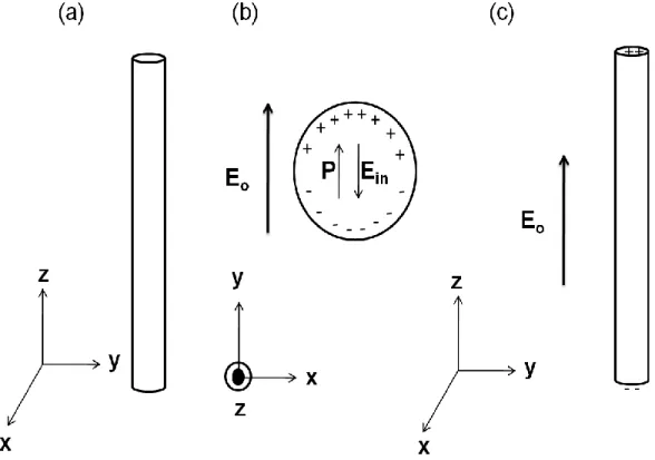
On another hand, it is also interesting to reduce the zero-point fluctuations of the field to suppress the coupling to the continuum of „useless‟ modes. The structures that will be studied in this thesis are dielectric cylinders, made of a high refractive index material (GaAs, n=3.45). As illustrated in Figure 1.11, a dielectric screening effect reduces to a large extent the field inside the wire, for polarizations perpendicular to the wire axis. Briefly, the incident electric field polarizes the wire, leading to the appearance of surface charges which in turn generate a field opposite to the incident one. If the refractive index contrast between the wire and its surroundings is high enough, the total field inside the wire is considerably reduced.
Figure 1.11: Illustration of the dielectric screening effect in a photonic nanowire.
The plot is a map of the total electrical field amplitude. The white solid line represents the circumference of the wire.
14 As a remark, one can also mention that a finite photonic bandgap structure does not lead to a „true‟ photonic bandgap. The action of Bragg reflection can be understood as a screening of the mode incident on the structure.
1.3.2 Two major strategies to control SE
In this section, we examine two strategies to obtain single-mode emission. The first one is resonant; it uses a resonant optical microcavity and has been inspired by atomic physics. The second approach, which has been used in this thesis, uses a waveguide and provides a broadband operation range.
1.3.2.1 Resonant SE control: the Purcell effect
In 1946 E.M. Purcell [53] proposed that the emitter‟s spontaneous rate could be dramatically enhanced when it is inserted in a resonant cavity; the so-called Purcell effect leads to a selective enhancement of M, the SE rate into the
cavity mode. Choosing the SE rate 3D of an emitter embedded in bulk GaAs as
a reference, the maximum magnitude of this effect is captured by the Purcell factor F=M3D. F is calculated for a maximum coupling to the cavity mode
(on-resonance monochromatic emitter, emitter located on a maximum of the electrical field, linear dipole of the transition aligned along the electrical field). In these conditions, 3 2 n V Q 4 3 F , (1.3)
with the emission wavelength in vacuum, Q the quality factor of the mode and V the mode volume. Achieving a high Purcell factor thus requires a cavity able to store the photons over long times (high Q) and to confine the electromagnetic field over small volumes (small V).
In the early 1990s, the progress of the growth of QD (artificial atoms), and the simultaneous development of processing at sub-micron scale has triggered the development of cavity-emitter systems in semiconductors. Several geometries have been proposed and developed; among the best candidates one can cite: micropillar [27, 54-56], VCSEL-like cavities [57, 58], microdisk [30, 59] and 0D defect in photonic crystal membranes [60-64]. These structures are presented in Figure 1.12 (a) and (b). In micropillar, VCSEL-like and microdisk cavities, the coupling to the continuum of „radiative‟ modes is not affected significantly (i.e.~ 3D). In addition to Purcell effect, 0D defect in photonic crystal
15
Figure 1.12: Various approaches to control the spontaneous emission, (a)
Micropillar [56] and Microdisk [30], (b) Photonic nanocavity [61], (c) Photonic crystal waveguide [76] and (d) Photonic nanowire. Here Figure (a) and (b) represent the 0D photonic system while Figure (c) and (d) represents 1D photonic system.
Purcell-based single-photon sources:
To realize a bright single-photon source with a collection of light in the far-field, or to couple the emission to a monomode optical fiber, the control over the far-field radiation pattern of the cavity is also very important. To this respect, VCSEL-like or micropillar cavities, whose fundamental optical mode features a Gaussian structure [64], are the most advanced to date. By using this strategy, the first optically pumped solid state single-mode single-photon source has been demonstrated [55, 65, 66].as well electrical pumped SPS [75]. This approach has also been realized the situation when a single emitter is strongly coupled to the single optical mode of cavity under optical [67, 68] and electrical pumping [69]. In terms of global efficiency, photonic crystal structures are less advanced [70, 71], because of the difficulty to control the far-field emission pattern. Several solutions have been proposed, such as the efficient on-chip coupling to a waveguide [72] or near-field tunnelling to a monomode fiber [73]. One can also engineer the PhC
16 slab nanocavity geometry (by shifting holes or changing holes sizes etc), which can funnel the cavity mode into free space with reduce divergence angle. In principle unidirectional emission can be achieved by placing a mirror beneath the slab cavity [74]. Various single photon source based on this approach is shown in the Figure 1.13.
Figure 1.13: Purcell effect based single photon sources with, (a) Micropillar
cavity [65,66], (b) Oxide aperture cavity [54], (c) Photonic crystal nanocavity [62], all of three are optically pumped and (d) Electrically pumped single photon source [75].
1.3.2.2. Limits of a resonant approach
The Purcell effect is a resonant effect; it is therefore limited to the narrow operation bandwidth of the cavity. For a cavity with Q>1000 operating with a resonance in the 1 µm wavelength range, the operation bandwidth of the system is below 1 nm. Such a resonant effect implies several constraints. The first one is practical: given the inhomogeneous distribution (50 nm) of self-assembled InAs QD, and the temperature tuning range of 1 nm, only a small fraction of the QDs will spectrally match the cavity. Moreover, this strategy is restricted to monochromatic emitters (with respect to the cavity linewidth): it will not be efficient for spectrally-broad emitters. For the realization of sources of entangled-photon pairs using a QD, one has to collect simultaneously the exciton and bi-exiton transition of a QD (1-3 nm of detuning in a typical InAs/GaAs QD). In the context of single-photon emission, non-resonant cavity feeding effect can spoil the purity of single-photon emission (for a strong, non-resonant excitation); these non-trivial effects will be discussed later on in the manuscript.
A supplementary drawback is the sensitivity of the radiation pattern of high-Q microcavities. It has been reported that the radiation pattern of high-Q
17 micropillars is partially spoiled by extrinsic loss mechanisms such as scattering by sidewall roughness [45]. Therefore the maximum efficiency of the source is limited to 40% for optically pumped QD-micropillar [54, 55, 65]. These considerations are general: after more than a decade of intense research, the practical realization of single photon source relying on the use of a micro / nano -resonator and offering extraction efficiencies close to 100% remains a challenge. All these considerations motivate the quest for non-resonant approaches to control spontaneous emission. We describe two examples in the following.
1.3.2.3. First examples of SE control in a waveguide
To obtain a non resonant SE control, a possible idea consists in increasing the dimensionality of the photonic structure from 0D to 1D; in other word, to use a waveguide to control the SE of an embedded emitter.
Waveguide in photonic bandgap structures:
A convincing experiment has been performed on a waveguide defined in a photonic crystal membrane (see Figure 1.14) [76], following a theoretical proposal [77, 78]. In this structure, the good coupling to the guided mode is ensured by a tight lateral confinement of this mode. The coupling to the 3D continuum of „leaky‟ modes is suppressed thanks to a photonic bandgap effect. These two effects are clearly shown in Figure 1.12 (c). In photonic crystal waveguides a large β-factor in excess of 95% has been theoretically predicted for the two in-plane QD dipole orientations over a 40 nm bandwidth [79], β-factors of up to 0.89 over a 20 nm bandwidth have been experimentally inferred for InAs QDs embedded into GaAs photonic crystal waveguide[76].
Figure 1.14: Spontaneous emission control mechanisms of photonic crystal
18 As a remark, it is possible to further increase the coupling to the guided mode by playing with the dispersion relation of this mode. In the slow light regime (low group velocity vg), the light-matter coupling is increased (the SE rate scales as
1/vg) [80]. However, this strategy restricts the operation bandwidth of the system.
Plasmonic waveguides:
Plasmonic waveguides offer another route for broadband SE control [81]. The coupling of an emitter to a metal nanowire, illustrated in Figure 1.15, has been demonstrated in Ref. [82]. This approach requires positioning the emitter very close to the metal surface (a few 10 nm), which can lead to the onset of non-radiative decay channels and quench the radiative efficiency of the emitter. In addition, the propagation of plasmons is lossy.
Figure 1.15: Spontaneous emission control in plasmonics waveguides [82].
1.4 This thesis: fiber-like photonic nanowires to realize
efficient sources of quantum light
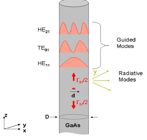
In this thesis, we demonstrate a new 1D photonic system to control SE: a fiber-like, vertical photonic nanowire (see Figure 1.16). This structure offers a unique combination of high-, low losses, and controlled far-field pattern, provided that a proper engineering of the wire ends is conducted.
19
Figure 1.16: Photonic nanowire system with different shapes, (a) Regular taper
photonic nanowire, (b) Elliptical photonic nanowire, and (c) Inverted taper based photonic wire.
1.4.1
Fiber-like photonic nanowiresMore precisely, a dielectric photonic wire is a waveguide made of a high refractive index material, surrounded by a cladding with a low refractive index. They were first introduced in the context of planar ring microlasers [83]. We consider here a vertical, cylindrical photonic nanowire, a configuration more adapted to efficient light collection in the far-field. In our case, the wire is made of GaAs (n=3.45 at 950 nm) and is surrounded by air or vacuum (n=1). The wire embeds a single layer of self-assembled InAs QDs (typical emission wavelength in vacuum around 950 nm). The high refractive index contrast between the wire and the cladding has two important consequences. It first allows confining the guided mode very tightly, which ensures a good coupling to the embedded emitter. Second, a dielectric screening effect suppresses to a large extent the coupling to the 3D continuum of „radiative‟ modes. This results in an efficient SE control, with -factors exceeding 90% over a bandwidth larger than 100 nm at 950 nm.
Next, one has to collect efficiently the guided photons with a microscope objective located above the wire. For this goal, the two ends of the wire are carefully engineered. The photons emitted downward are reflected back into the guided mode with an integrated mirror, made of gold and silica. The upper wire
20 end features a conical tip, designed to deconfine progressively the guided mode into the cladding, in order to obtain a more directive far-field emission pattern. The main experimental results described in this manuscript are:
- The detailed investigation of SE in photonic nanowires, in particular the demonstration of the inhibition of the SE into the continuum of „radiative‟ modes - The realization of a bright photon source, featuring a record single-photon emission efficiency (72% into the first collecting lens), combined with a pure single-photon emission.
- The realization of a new generation of trumpet-like photonic wires, that should bring the out-coupling efficiency closer to 100% (experiments are in progress).
- The realization and study of photonic wires featuring an elliptical section. In this geometry, the electromagnetic environment seen by an embedded emitter is dominated by a single mode, with a linear polarization oriented along the ellipse major axis.
1.4.2 Outline of the thesis
The thesis will cover all the aspects associated with the above-mentioned realizations: design, micro fabrication and optics experiments. After this introductory chapter, the thesis is organized as follows:
Chapters 2 describes the design of two high efficiency single-photon sources
based on quantum dots embedded into photonic nanowires. In the first part of chapter, we analyse the mechanisms of spontaneous emission control in photonic nanowires and optimize the geometry to achieve a high -factor. Then we optimize far field to increase the extraction efficiency by engineering the nanowire ends. We introduce a high reflectivity bottom mirror (combination of gold and silica) to reflect the photon emitted towards the substrate. To reduce the far field divergence we introduce two possibilities: regular tapering of the top facet and inverted taper photonic wires. These two geometries provide high efficiency single-photon emission.
Chapter 3 describes the fabrication of these two photonic nanowire structures. It
begins with the description of the design details and epitaxial sample details for both structures. Then we discuss flip chip process to realize the high reflectivity composite bottom mirror for both structures. Afterward we discuss the fabrication
21 of the regular taper structures including the mask requirements and optimization of the etching. In the last part of the chapter we describe the fabrication process of the second geometry, specially discuss the etching mask and etching condition to realize this highly anisotropic structure.
Chapter 4 describes the optical performances of regular taper device. First we
probe the SE control process of the photonic nanowire. We experimentally show that this structure provides moderate coupling of emitter to the fundamental guided mode. Then we demonstrate that the coupling to the radiative modes is strongly inhibited thanks to the dielectric screening effect. This geometry provides a broadband SE control. In the second part of the chapter, we demonstrate the performance of the device in context of single photon emission. We show that this structure provides the highly pure and highly efficient single photon emission in comparison to state-of-the-art cavity-based devices.
Chapter 5 introduces photonic nanowires with an elliptical cross section, which
provide an electromagnetic environment dominated by a single guided mode, with a linear polarization oriented along the ellipse major axis. The first section presents the theoretical analysis and the optimization of the SE coupling factor . Afterward we describe the fabrication process. In the last part of this chapter, we represent the optical characterization of this device. This structure provides the broadband and efficient polarization control which leads to the truly single mode spontaneous emission.
Chapter 6 concludes this thesis with a summary of the results and their
relevance to the field of quantum information processing.
1.5 Contribution to the experimental work
During my PhD, I was mostly involved in the microfabrication in clean room for the optimization of the fabrication of the devices. The developments I conducted are fully developed in Chapter 3 and 5; they are briefly summarized below:
- Flip-chip process, to obtain a GaAs membrane on the top of a high reflectivity mirror (combination of gold and silica). This was the first critical step of our device fabrication, and has been used for numerous other projects.
22
- E-beam lithography (mask design using L-EDIT and operation of the
JEOL 6300 FS e-beam system)
- Optimization of the dry etching (etching parameters and hard mask): this step, which defines the shape of the structures, is critical. We were able to realize photonic wires with a conical top taper, trumpet like structures and finally wires with a well-controlled elliptical cross-section. The main challenge was to control the shape of the wire while preserving smooth sidewalls.
Co-workers acknowledgment:
The work presented in this manuscript has been done under the supervision of Julien Claudon and Jean-Michel Gérard. It has required the joint efforts of people with complementary expertises. The simulation of the structures for design optimization has been performed by Yuntian Chen, Niels Gregersen and Jesper Mork (DTU Fotonik, Lyngby, Denmark) and Inbal Friedler, Ivan Maksymov, Jean-Paul Hugonin, Christophe Sauvan and Philippe Lalanne (Institut d‟Optique, Orsay, France).
The experimental work has been entirely conducted in the team „NanoPhysics and SemiConductors‟.
- Growth by molecular beam epitaxy of GaAs layer with embedded
self-assembled InAs QDs: Maela Bazin,Périne Jaffrennou and Emmanuel Dupuy. - Nanofabrication, clean room processing: Julien Claudon and myself
- Optics experiments: Joël Bleuse, Mathieu Munsch and Megan Creasey
Besides the realizations presented in this thesis, I was also involved into other projects: they are listed below:
Electrically pumped single-photon source based on a photonic nanowire:
This project is the natural prolongation of the work presented in this thesis. The realization of this single-photon LED is relatively complex: I was involved in the definition of a suitable process flow and its optimization. We have performed 4 steps e-beam lithography alignment with an alignment accuracy of about 20 nm and the optimization of the n- and p-type contact recipes for GaAs. The first device (no bottom mirror) is almost ready for the experiment.
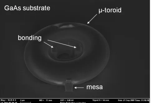
Coupling of InAs/GaAs quantum dots (QD) to whispering gallery mode (WGM) supported by a high-Q microtoroid cavity:
23 This project was my initial PhD project: the motivation was to couple a nice artificial atom to the ultra-high Q modes that are supported by a fused silica microtoroid. I was involved in the optimization of the fabrication of semiconductor QDs mesa, the device assembling and optical characterization. The mesas were realized using a top-down approach (e-beam lithography and etching). The fused silica microtoroids were provided by Jean-Baptiste Jager (SP2M/SINAPS). We realized the device by assembling the microtoroid and mesa on the same chip with the help of Focussed Ion Beam (FIB) equipped with a manipulation tip (with Violaine Salvador (SP2M/LEMMA) and Marlène Terrier (SP2M/NPSC)) which is shown in Figure 1.17. In optical characterization, this device demonstrated a coupling between the QD and WGM of microtoroid, with relatively low optical Q-factors, in the 1000 range.
Figure 1.17: SEM image of quantum dots mesa and microtoroid assembly
realized on the same chip by FIB manipulation.
Whispering gallery mode lasing in a micropillar cavity (room temperature operation with electrical pumping):
This laser is a first step toward the realization of a compact and innovative THz radiation source, which exploits the non-linear generation of THz, through the frequency difference of two near infrared WGMs. The epitaxial samples were provided by Wurzburg University, and I conducted the fabrication (single e-beam lithography step to define the top contact and the etching mask + participation to
24 the optimization of the etching). The laser has demonstrated lasing at 300K, under electrical pumping (wavelength around 920 nm). Figure 1.18 shows the SEM image of the realized device with the electrical contacts scheme and we drilled the annular trenches with FIB to reduce the number of QDs uncoupled to WGM of pillars that leads to the reduction of lasing threshold.
Figure 1.18: SEM image of Whispering gallery mode laser based on micropillar
cavity and the electrical contacts scheme of device.
Coherent X-ray diffraction imagining of single InAs monolayer / InAs QDs embedded in GaAs nanowire:
This project, in collaboration with Francesca Mastropietro, Vincent Favre Nicolin (SP2M/NRS) and Joel Emery (SP2M/NPSC), targets the localisation of single heterostructures (InAs QD or QW), using coherent X-ray diffraction (experiment performed at the SYNCHROTRON, Grenoble). To this end, a key requirement is to isolate the signal of the wire from the one of the background most probably from the substrate. We thus exploited the know-how developed in the context of photonic wire single-photon sources, to define wires on a Silicon (Si) substrate by using 3 m thick Silicon nitride intermediate layers. Figure 1.19
25 shows the SEM images of nanowires defined on the top of Silicon nitride layer lying on the Si-substrate.
Figure 1.19: SEM image of the GaAs nanowire with embedded InAs
monolayer/InAs QDs lying on the top of Si3N4 layer.
References
1. A. Ekert D. Bouwmeester and A. Zeilinger, “The Physics of Quantum
Information.” Springer Verlag, (Berlin), (2000).
2. I. L. Chuang and M.A. Nielsen, “Quantum Computation and Quantum
Information,” Cambridge University Press, (2000).
3. A. Shields, “Semiconductor quantum light sources,” Nature Photonics 1, 215
(2007).
4. E. Knill, R. Laflamme, and G. J. Milburn, “A scheme for efficient quantum
computation with linear optics," Nature 409, 46-52 (2001).
5. N. Gisin, G.G Ribordy, W. Tittel, and H. Zbinden, “Quantum cryptography,” Rev. of Mod. Phys. 74(1), 145 (2002).
6. E. Waks, K. Inoue, C. Santori, D. Fattal, J. Vuckovic, G.S. Solomon, and Y. Yamamoto, “Secure communication: Quantum cryptography with a photon
turnstile, “ Nature 420, 762 (2002).
7. P. Kok, W.J .Munro, K. Nemoto, T.C. Ralph, J. P. Dowling, and G.J. Milburn, “Linear optical quantum computing with photonic qubits,” Rev. Of Mod. Phys.
26 8. H. J. Briegel, W. Dur, J.I. Cirac, and P. Zoller, “Quantum repeaters: The role
of imperfect local operations in quantum communication,” Phys. Rev. Lett. 81,
5932 (1998).
9. B. Lounis and M. Orrit, “Single-photon sources,” Rep. Prog. Phys. 68, 1129 (2005).
10. A. Muller, T. Herzog, B. Huttner, W. Tittel, H. Zbinden, and N. Gisin, “Plug
and play systems for quantum cryptography,” Appl. Phys. Lett. 70, 793
(1997).
11. W. T. Buttler, R. J. Hughes, P. G. Kwiat, et al., “Free-space quantum-key
distribution,” Phys. Rev. A 57, 2379 (1998).
12. G. Brassard, N. Lutkenhaus, T. Mor, and B. C., Sanders, “Limitations on
practical quantum cryptography,” Phys. Rev. Lett. 85, 1330 (2000).
13. S. A. Castelletto and R. E. Scholten, “Heralded single photon sources: a route
towards quantum communication technology and photon standards,” Eur.
Phys. J. Appl. Phys. 41, 181 (2008).
14. C. K. Hong and L. Mandel, “Experimental realization of a localized one photon
state,” Phys. Rev. Lett. 56, 58 (1986).
15. G. Brassard, N. L¨utkenhaus, T. Mor, and B. C. Sanders, “Limitations on
practical quantum cryptography,” Phys. Rev. Lett. 85, 1330 (2000).
16. H. J. Kimble, M. Dagenais, and L. Mandel, “Photon antibunching in resonance
fluorescence,” Phys. Rev. Lett. 39, 691 (1977).
17. A. Kuhn, M. Hennrich, and G. Rempe, “Deterministic single-Photon source for
distributed quantum networking,” Phys. Rev. Lett. 89, 067901 (2002).
18. M. Keller, B. Lange, K. Hayasaka, W. Lange, and H. Walther, “Continuous
generation of single photons with controlled waveform in an ion-trap cavity system,” Nature 431, 1075 (2004).
19. F. Diedrich and H. Walther, “Nonclassical radiation of a single stored ion.
Phys. Rev. Lett.,” 58(3), 203 (1987).
20. T. Basche, E. W. Moerner, M. Orrit, and H. Talon, “Photon antibunching in the
fluorescence of a single dye molecule trapped in a solid,” Phys. Rev. Lett. 69,
1516 (1992).
21. B. Lounis and W. E. Moerner, “Single photons on demand from a single
molecule at room temperature,” Nature 407, 491 (2000).
22. R. Brouri, A. Beveratos, J. P. Poizat, and P. Grangier, “Photon antibunching
in the fluorescence of individual color centers in diamond,” Opt. Lett. 25, 1294
(2000).
23. C. Kurtsiefer, S. Mayer, P. Zarda, and H.Weinfurter, “Stable solid-state source
of single photons,” Phys. Rev. Lett. 85, 290 (2000).
24. D. A. Simpson, E. Ampem-Lassen, B. C. Gibson, S. Trpkovski, F. M. Hossain, S. T. Huntington, A. D. Greentree, L. C. L. Hollenberg and S. Prawer, “ A highly efficient two level diamond based single photon source,‟ Appl. Phys. Lett. 94, 203107 (2009).
25. P. Michler, A. Imamoglu, M. D. Mason, P. J. Carson, G. F. Strouse, and S. Buratto, “Quantum correlation among photons from a single quantum dot at
27 26. A. J. Bennett, D. C. Unitt, P. Atkinson, D. A. Ritchie, and A. J. Shields, “High
performance single photon sources from photolithographically defined pillar microcavities,” Opt. Exp. 13, 50 (2005).
27. J.-M. Gérard, and B. Gayral, “Strong Purcell effect for InAs quantum boxes in
three-dimensional solid-state microcavities,” J. Lightwave of Technology 17,
2089 (1999).
28. J.-M. Gérard, “Solid-State Cavity-Quantum Electrodynamics with
Self-Assembled Quantum Dots,” Single quantum dots: Fundamentals, applications and new concepts 90, 269 (2003).
29. C. Santori, M. Pelton, G. Solomon, Y. Dale, and Y. Yamamoto, “Triggered
single photons from a quantum dot,” Phys. Rev. Lett. 86, 1502 (2001).
30. P. Michler, A. Kiraz, C. Becher, W.V. Schoenfeld, P.M. Petroff, L.D. Zhang, E. Hu, and A. Imamoglu, “A quantum dot single-photon turnstile device,” Science
290, 2282 (2000).
31. Z. L. Yuan, B. E. Kardynal, R. M. Stevenson, A. J. Shields, C. J. Lobo, K. Cooper, N. S. Beattie, D. A. Ritchie, and M. Pepper, “Electrically driven
single-photon source,” Science 295, 102( 2002).
32. D. Bimberg, M. Grundmann, and M.M. Ledenstov, “Quantum Dot
Heterostructures,” Wiley, Chichester, (1999).
33. Y. Masumoto, T. Takagahara, “Semiconductor quantum dots: physics,
spectroscopy and applications,” Springer, (2002).
34. G. Cassabois, “Origines et limites du modèle de l'atome artificiel pour une
boîte quantique de semiconducteurs,” HDR Thesis, Universite Paris VI (2006).
35. B. Ohnesorge, M. Albrecht, J. Oshinowo, A. Forchel, and Y. Arakawa, “Rapid
carrier relaxation in self-assembled InxGa1-xAs/GaAs quantum dots,” Phys.
Rev. B 54, 11532 (1996).
36. Y. Masumoto, T. Takagahara, “Semiconductor quantum dots: physics,
spectroscopy and applications,” Springer, (2002).
37. P. Michler, editor, “Single Quantum Dots: Fundamentals, Applications and
New Concepts,” Springer-Verlag, Berlin, (2003).
38. O. Benson, C. Santori, M. Pelton and Y. Yamamoto, “Regulated and
Entangled Photons from a Single Quantum Dot,” Phys. Rev. Lett. 84, 2513
(2000).
39. C. Kammerer, C. Voisin, G. Cassabois, C. Delalande, Ph. Roussignoal, F. Klopf, J. P. Reithmaier, A. Forchel and J.-M. Gérard, “Line narrowing in single semiconductor quantum dots: Toward the control of environment effects,” Phys. Rev. B 66, 041306(R) (2002).
40. I. Favero, A. Bertelot, G. Cassabois, C. Voisin, C. Delalande, Ph. Roussignol, R. Ferreira and J.-M. Gérard, “Temperature dependence of the zero-phonon
linewidth in quantum dots : An effect of fluctuating environment,” Phys. Rev. B
75, 073308 (2007).
41. L. Besomes, K. Kheng, L. Marsal and H. Mariette, “Acoustic photon
broadening mechanism in single quantum dot emission,” Phys. Rev. B 63,