Constructing Multifunctional Virus-Templated Nanoporous
Composites for Thin Film Solar Cells: Contributions
of Morphology and Optics to Photocurrent Generation
The MIT Faculty has made this article openly available. Please share how this access benefits you. Your story matters.
Citation Dorval Courchesne, Noémie-Manuelle, Matthew T. Klug, Kevin J. Huang, Mark C. Weidman, Victor J. Cantú, Po-Yen Chen, Steven E. Kooi, et al. “Constructing Multifunctional Virus-Templated
Nanoporous Composites for Thin Film Solar Cells: Contributions of Morphology and Optics to Photocurrent Generation.” The Journal of Physical Chemistry C 119:25 (June 10, 2015), p. 13987–14000.
As Published http://dx.doi.org/10.1021/acs.jpcc.5b00295
Publisher American Chemical Society (ACS)
Version Author's final manuscript
Citable link http://hdl.handle.net/1721.1/102981
Terms of Use Article is made available in accordance with the publisher's policy and may be subject to US copyright law. Please refer to the publisher's site for terms of use.
Constructing Multifunctional Virus-Templated Nanoporous
Composites for Thin Film Solar Cells: Contributions of
Morphology and Optics to Photocurrent Generation
Noémie-Manuelle Dorval Courchesne,1,2† Matthew T. Klug,2,3† Kevin J. Huang,4 Mark C.
Weidman,1 Victor J. Cantu,1 Po-Yen Chen,1,2 Steven E. Kooi,5 Dong Soo Yun,2 William A.
Tisdale,1 Nicholas X. Fang,3 Angela M. Belcher,2,4,6* and Paula T. Hammond1,2*
1Department of Chemical Engineering, Massachusetts Institute of Technology, Cambridge, MA
02139, United States. 2The David Koch Institute for Integrated Cancer Research, Massachusetts
Institute of Technology, Cambridge, MA 02139, United States. 3Department of Mechanical
Engineering, Massachusetts Institute of Technology, Cambridge, MA 02139, United States.
4Department of Materials Science and Engineering, Massachusetts Institute of Technology,
Cambridge, MA 02139, United States. 5The Institute for Soldiers Nanotechnologies,
Massachusetts Institute of Technology, Cambridge, MA 02139, United States. 6Department of
Biological Engineering, Massachusetts Institute of Technology, Cambridge, MA 02139, United States.
† These authors contributed equally to this work.
KEYWORDS. M13 bacteriophage, bulk heterojunction solar cells, porous titania, lead-sulfide quantum dots, plasmonics, metal nanoparticles
ABSTRACT
Biotemplates, such as the high aspect ratio M13 bacteriophage, can be used to nucleate noble metal nanoparticles and photoactive materials such as metal oxides, as well as organize them into continuous structures. Such attributes make them attractive scaffolds for solar applications requiring precise organization at the nanoscale. For instance, thin film solar cells benefit from nanostructured morphologies that aid light absorption and carrier transport. Here, we present a biotemplating strategy for assembling nanostructured thin film solar cells that enhance the generated photocurrent through two features: (1) a nanoporous and continuous M13 bacteriophage-templated titania network that improves charge collection, and (2) the incorporation of metal nanoparticles within the active layer of the device to improve light harvesting. We demonstrate our ability to construct virus-templated solar cells by applying this strategy to depleted titania–lead sulfide quantum dot (PbS QD) bulk heterojunctions. The titania morphology produced by our biotemplate allows charges to be efficiently collected from the bulk of the active material and light that is otherwise poorly absorbed by the QDs to be harvested using metal nanoparticles that exhibit plasmon resonances in the visible range. We show that high aspect-ratio bacteriophages provide a structural template for synthesizing titania networks with tunable porosity, into which PbS QDs are infiltrated to create photoactive nanocomposites suitable for photovoltaics. Upon optimization, the generated photocurrent and power conversion efficiency of the bacteriophage-templated devices demonstrate a 2-fold improvement over control devices made with randomly organized titania nanoparticles. When the virus is complexed with gold nanospheres (Au NPs), silver nanospheres (Ag NPs), or silver nanoplates (Ag NPLs) during
current density and power conversion efficiency by 16% and 36.5%, respectively, over virus-based devices without NPs. The observed trends in photocurrent enhancement match well with numerical predictions and the role of the nanostructured morphology on the device optics was computationally explored. The challenges overcome in this work could be extended to other heterojunction devices, such as hybrid systems involving conducting polymers, as well as other biologically-templated electronics.
INTRODUCTION
Strategies for improving solar cells generally fall into one of two categories; the first focuses on synthesizing better materials, while the other focuses on generating architectures that optimize performance. New materials with improved photovoltaic properties are constantly emerging; however, device architectures that can capitalize on a material’s strengths, while compensating for its weaknesses are necessary for maximizing the performance of any given solar cell. For instance, the careful selection of materials in heterojunction solar cells can maximize photovoltage and reduce recombination, whereas nanostructured architectures can enhance photocurrent by improving light absorption and carrier collection efficiencies. Such nanostructured morphologies have been shown to improve the performance of several heterojunction types, including organic,1 2 inorganic,3 hybrid,4 5 and colloidal quantum dot
devices.678910 Likewise, optical structures such as gratings,1112 plasmonic nanoparticles,13 1415 16 and photonic crystals 17 have been used to improve the ability of photovoltaics to harvest light,
and thus offer a second pathway for increasing photocurrent. Therefore, a well-designed architecture that complements excellent active materials is required to achieve champion photovoltaic performance.
Biotemplating is a bottom-up approach to constructing nanostructures that uses biological material as a scaffold to nucleate inorganic material. By programming the biotemplate at the genetic level to express proteins with specific functionality, multifunctional composites can be assembled and further mineralized for use in non-biological applications. One of the most well-characterized and versatile biotemplates is the filamentous M13 bacteriophage, which has been used previously to (1) bind a variety of inorganic nanomaterials including carbon nanotubes,18
graphene,19 and metal nanoparticles,202122 (2) assist in the nucleation and templating of inorganic
materials such as metals, semiconductors,22 23 polymers,24 and complex metal-oxides,25 and (3)
act as building blocks for the assembly of hierarchical structures.222324 All of these virus-templated
materials exhibit nanowire-like morphologies consistent with the filamentous structure of the individual virions. The availability of surface functional groups allows M13 bacteriophages to be easily cross-linked to generate porous scaffolds, films, and gels suitable for energy applications. As previously demonstrated in dye-sensitized solar cells (DSSCs), virus hydrogels and virus-polymer composites are able to create percolation pathways that improve electron diffusion lengths by acting as a scaffold for the nucleation of titania.2326 Furthermore, genetically encoding the virus
to bind with either carbon nanotubes18 or gold nanoparticles23 has enhanced device performance
by respectively improving either the charge collection efficiency or light harvesting ability of the photoanode.
The aim of this work is to use the M13 bacteriophage to construct solution-processable thin film solar cells that are light weight, solid-state alternatives to the thicker, liquid-based dye-sensitized counterparts. This class of devices uses heterojunctions comprised of either organic or inorganic materials to generate photovoltage and extract charges to the proper electrodes.
lengths than dye-sensitized solar cells, and thus require thinner films with feature sizes that match these length scales. Therefore, building a virus-templated morphology suitable for use in solution-processed solar devices that are only a few hundred nanometers thick requires synthesis techniques that offer more precise control over device thickness and porosity than the methods previously employed for building DSSC photoanodes. The procedures used to synthesize the tens of microns thick photoanodes necessary for DSSCs resulted in rough films with macroscopic pores that varied in size throughout the film thickness, which are unsuitable for thin film devices. In contrast, we have previously reported a method to assemble nanoporous bacteriophage-based anatase titania films of controllable thickness and uniform porosity by combining a covalent cross-linking process with layer-by-layer (LbL) assembly.22 It was also shown that by binding metal nanoparticles to the
virus prior to film assembly, the particles could be evenly distributed throughout the final nanoporous anatase titania film without aggregation. Using this framework, we aim to construct a multifunctional device architecture that is capable of enhancing photocurrent generation in a variety of solution-processed thin film solar devices. As illustrated by Scheme 1, our two-fold approach consists of (1) controllably constructing a M13 bacteriophage-based nanoporous titania nanowire network with nanoscale features to efficiently collect and transport charges from the bulk material, and (2) loading it with plasmonic metal nanoparticles capable of increasing light harvesting via localized surface plasmon resonance (LSPR).
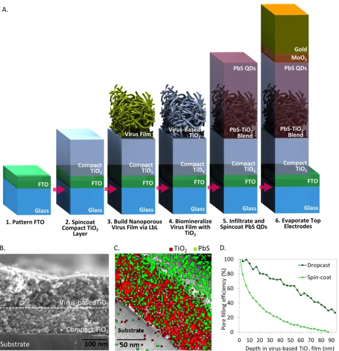
Scheme 1. Illustration of two fold-strategy employed in building a virus-based nanoscale device
architecture, as applied to PbS QD solar cells, to enhance the photocurrent generation over a randomly-organized geometry. A. The control device has a disorganized geometry that consists of a layer of PbS QDs infiltrated into a porous layer of titania nanoparticles. The percolation pathways for electrons can be circuitous depending on how the TiO2 NPs sinter together. B. Virus-templated
titania network provides a blended heterojunction morphology that allows photogenerated charges to be collected from QDs that have infiltrated into the network and provides more direct pathways to conduct electrons. C. Metal nanoparticles act as nano-antennas to concentrate light in their near-field region, thereby producing a higher photon flux on nearby QDs and an increased rate of carrier generation.
This strategy is applicable to many different solution-processed solar cell types because (1) anatase titania is popularly employed as the n-type component in hybrid organic-inorganic, colloidal quantum dot, and perovskite systems, (2) nanostructured titania is commonly used to assist in charge extraction in bulk-heterojunction devices and in perovskite solar cells,27 and (3)
choice to capture light that is poorly absorbed for any given active material. To evaluate the feasibility of our approach and the suitability of the multifunctional virus-based films for solid-state thin film solar cells, we have chosen to assemble colloidal quantum dot bulk heterojunction solar cells. This is a class of solid-state photovoltaic devices that are low-cost, compatible with solution-processing methods, and have recently demonstrated efficiencies as high as 9.2%.6, 2829 30 Specifically, lead sulfide quantum dots (PbS QDs) are excellent active materials for solar cells
because they are efficient charge transporters, their band gaps can be tuned throughout the infrared spectrum, their band edges can be modified with various ligand molecules,31 and they are often
paired with anatase titania to form a heterojunction.
Traditionally, PbS QDs are stacked on top of a nonporous titania film to form a depleted heterojunction. In order to extract carriers efficiently in this planar device, the QD film thickness must be thinner than the carrier collection length (~200 to 250 nm), which is the sum of the depletion width and the minority carrier diffusion length.32 On the other hand, complete light
absorption requires that the QD film thickness be greater than the absorption length (>1 μm). Instead, a bulk heterojunction structure can be constructed by infiltrating QDs into nanostructured titania, which can extend the width of the depletion region and allow for more light to be absorbed with thicker QD films. However, these structures are more prone to trap-assisted recombination at defects if the conduction pathways are tortuous and if the interfacial surface area is high. For this reason, nanowire-based titania morphologies that provide continuous and direct pathways for charge transport are advantageous over disorganized mesoporous nanoparticle films commonly used in solution-processed solar cells.9 29 It has been shown that using an array of titania7 833 or
zinc oxide6 nanopillars or nanowires infiltrated with PbS quantum dots enhances the device
extended depletion zones overcome any undesirable increases in non-radiative recombination that result from a larger interfacial area between the active material and the titania nanostructures.
Our plasmonic virus-templated porous composite is rationally designed to generally compensate for the weaknesses of photoactive materials with relatively short lifetimes. Specifically for titania-PbS QD depleted bulk heterojunctions, our system offers the following advantages: first, the highly porous film allows for substantial infiltration of QDs into the titania networks, thereby extending the depletion region of the device. 7 Second, compared to a porous
film made using a titania nanoparticle paste, the interconnected network of titania nanowires formed by the high aspect ratio viruses provides direct pathways for transporting charges from the bulk of the device to the electrodes. Likewise, forming titania along a high aspect ratio template like the M13 bacteriophage produces a smaller overall surface area compared to a porous film comprised of spherical particles, and is therefore expected to have less surface defects to promote non-radiative recombination. Third, PbS QDs suffer from an absorption spectrum that preferentially absorbs high energy photons. Therefore, it is susceptible to the classic tradeoff in solar cells between light harvesting and carrier collection, where thick active layers are required to absorb light throughout the visible and infrared ranges, but carrier generated in the quasi-neutral region are less likely to diffuse to the depletion region before recombining. By using the M13 bacteriophage to carry and assemble metal nanoparticles with plasmon resonances in the visible range within nanoporous films, photons at poorly absorbed wavelengths can be concentrated in the near-field surrounding the NPs and light harvesting is improved without further increasing the QD film thickness. Lastly, the uniformity and sub-wavelength pore size combined with the ability of the virus to evenly disperse metal nanoparticles throughout the film offers an ideal environment
simulations to theoretically evaluate how several metal nanoparticle types can enhance light absorption in the devices.
This work presents the overall process for constructing virus-based depleted bulk heterojunction PbS QD solar cells, with a focusing on the optimization of various critical steps to maximize device performance, such as (1) PbS QD infiltration into the titania pore network (2) surface preparation prior to assembly, (3) biomineralization time and control of the morphology, and (4) nanoparticle-virus complexation procedures with different nanoparticles including gold nanoparticles (Au NPs), silver nanoparticles (Ag NPs) or silver nanoplates (Ag NPLs). Through this optimization, we were able to diminish parasitic resistances and improve light harvesting in the devices, yielding enhanced photocurrents and power conversion efficiencies. By comparing a nanoparticle paste control device against our virus-based system, we demonstrate significant photocurrent enhancement and separate the contributions due to morphology and plasmon enhancement.
RESULTS AND DISCUSSION
The device assembly process is schematized in Figure 1A. On a patterned fluorine-doped tin oxide (FTO) substrate, a dense and compact layer of titania paste is first spin-coated, and acts as a hole blocking layer to prevent shorting of the device. After annealing this base layer at 500 °C, the viruses or virus-metal nanoparticle complexes are assembled via LbL, as previously described.22 Various methods to functionalize the titania surface and prepare it for virus
attachment can be employed, and will be discussed later. Once the virus film is constructed, it is coated with titania using titanium tetrachloride as the precursor, and annealed again to burn off the viruses and generate an anatase crystalline titania nanoporous film. PbS QDs with an average
diameter of 2.9 nm and a first excitonic absorption peak at 905 nm (𝐸𝑔= 1.37 eV) are then infiltrated into the pores of the film via dropcasting or spin-coating to create the titania-lead sulfide composite. Finally, a 25 nm thick hole transporting layer of MoO3 is thermally evaporated,
followed by a 100 nm thick gold electrode. The device area of the resulting solar cells is 0.0547 cm2.
A cross-section of the final titania film shows the difference in morphology between the compact titania nanoparticle base layer and the porous virus-templated titania film (Figure 1B). The porous virus-templated titania film exhibits interconnected mesh-like titania structures (See Figure S1 in Supporting Information for additional images), and was designed to be easily infiltrated with quantum dots. In addition, nanowire-like features can be observed in the top virus-based portion of the film, creating direct pathways for electrons to travel in the titania phase. The TEM film cross-section shown in Figure 1C demonstrates that a titania-lead sulfide composite is achieved after QD infiltration. The QDs not only infiltrate completely through the nanoporous virus-template titania network but also form a packed layer above it. Others have previously infiltrated PbS quantum dots into nanowire arrays,6348 but the inter-spacing of the nanowires (on
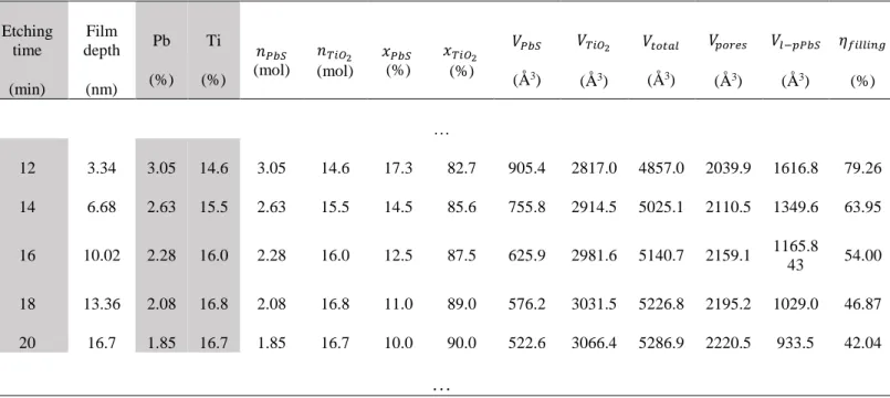
the order of 50 to 100 nm) was considerably larger than the pores of the virus-templated titania film presented here, which average 8.1 nm in diameter. Elemental mapping shows that a concentration gradient occurs within the infiltrated virus-templated film, and that the fraction of QDs gradually decreases with the film depth. This gradient was quantitatively measured for two successful infiltration methods, spin-coating and dropcasting. X-ray photoelectron spectroscopy (XPS) with depth profiling was used to monitor the atomic concentration of lead and titanium as a function of film depth and these atomic concentrations were converted to volume fraction of PbS
efficiency of pore filling with PbS QDs was calculated as a function of depth in the titania film, using a measured porosity of 42% for the titania film (see Figure 2B), and assuming the maximum possible QD packing density insides the pores is a loose random-packing configuration35 (see
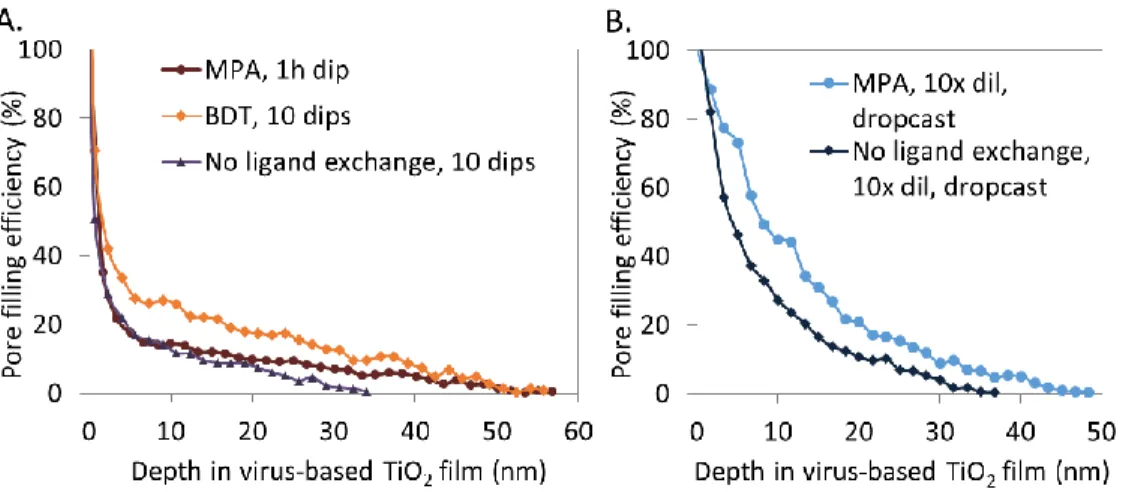
supporting information for details). The results are shown in Figure 1D. Dropcasting a dilute PbS solution at 50 mg/mL, followed by slowly drying at room temperature allows for more PbS QDs to infiltrate the film via capillary action, and maintains a high pore filling efficiency that is above 40% throughout the 100 nm thick virus-templated titania film (as opposed to using more dilute solutions or dip-coating methods, which result in a low PbS content within the pores, as shown in Figure S2 of supporting information). However, drying rings are observed on the surface of the film and poor film quality is produced when the dropcasting method is employed. In contrast, spin-coating produces a very smooth and uniform film. The concentration profile of PbS decreases more sharply with film depth, but the QDs still penetrate deeper than 80 nm into the virus-templated titania film. Therefore, a combination of these two methods is used to prepare the photovoltaic devices: PbS QDs are first dropcast onto the surface of the titania film, and then allowed to penetrate the film for 1 min; the solution is then spun off of the substrate at 2500 rpm in order to produce a smooth film, followed by a mercaptopropionic acid (MPA) ligand exchange and rinse. Subsequent layer of PbS quantum dot are then spin-coated and ligand exchanged in a layer-by-layer fashion.
To assess the impact of the virus nanocomposite system on device performance, we fixed the thickness of the titania layers and kept the PbS deposition procedure (concentration, ligand, number of deposited layers) consistent between devices. To determine these parameters, simple planar devices were fabricated using conventional procedures and a commercially available titania paste (Solaronix Ti-Nanoxide HT/SC) to create a compact titania layer. By varying the thicknesses
of both layers, it was established that a total titania thickness of approximately 200 nm is optimal, and that beyond five layers of spin-coated PbS QDs, no improvement is observed (See Figure S3 for details). In order to ensure full infiltration of PbS QDs within the virus-templated titania layer, we fixed the electron transporting compact titania base layer to 100 nm and the virus-templated titania layer to 100 nm, for a total of 200 nm of titania.
Figure 1. Virus-based titania-PbS QD composites are assembled via sequential
solution-processing to result in the final solar cells. A. Assembly process for virus-based solar cells via layer-by-layer assembly of viruses, titania nucleation of the virus template using a TiCl4 precursor,
PbS QD infiltration and film deposition, followed by thermal evaporation of MoO3 and gold top
electrodes. B. SEM image of the cross-section of a titania-coated virus film on a compact titania paste base layer. The dash line indicates the interface between the base layer and the virus-templated titania film. C. TEM image with elemental mapping (EDX) of lead sulfide quantum dots infiltrated into a porous virus-templated titania film constructed in a silicon substrate. D. Pore filling efficiency of loose-packed lead sulfide quantum dots as a function of depth in a virus-templated titania film, when the PbS QDs are either spin-coated or dropcast. A depth of 0 nm corresponds to the interface between the top PbS QD layer and the TiO2-PbS blend layer.
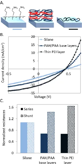
A critical design step in assembling photoactive materials using biomolecules is controlling the surface chemistry of inorganic components. The chosen surface functionalization method must provide uniform surface coverage with a high loading density of the biotemplate, but it must also involve reagents that can be completely degraded and removed from the device afterwards to avoid interfering with charge transport. In this work, M13 bacteriophages must be adsorbed or covalently attached to the titania base layer as a first step in the virus film assembly. After the film assembly and biomineralization with titania, the bacteriophages are burnt off at a temperature of 500 °C. Therefore, the reagents used for surface functionalization must also burn off at this temperature.
Three surface modifications were considered for functionalizing the titania base layer with a monolayer of viruses: silanization with (3-aminopropyl)trimethoxysilane (APTMES), construction of polymer base layers via electrostatic LbL assembly, and spin-coating a thin layer of a charged short chain polymer. These modifications are illustrated in Figure 2A, and the corresponding performance of each virus-based titania-PbS solar cell is shown in Figure 2B. The silanization method has the advantage of forming covalent amide bonds between the amine groups of the silane molecules and the carboxylic acid groups of the virus through a reaction catalyzed by 1-ethyl-3-(-3-dimethylaminopropyl) carbodiimide (EDC). However, APTMES can leave silica, silicon, polysiloxane and other silicon derivative residues after combustion at 500°C. In consequence, high series and low shunt resistances are observed for devices made using silanization, producing low fill factors. The high series resistance is likely due to the presence of insulating residues, such as silica, at the titania-substrate interface while the shunt resistance could be created by the presence of conducting residue, such as silicon, providing alternate pathways for
In contrast, polymers such as poly(allylamine hydrochloride) (PAH), poly(acrylic acid) (PAA), and polyethyleneimine (PEI) are excellent candidates to replace silanes because they burn off at temperatures below 500 °C, with the major combustion product being carbon dioxide in the gas phase.36 Using LbL assembly, cationic PAH and anionic PAA can be layered electrostatically
on an oxygen plasma-treated titania surface. We thus assembled 4.5 bilayers of PAH and PAA, ending with a top positively charged PAH layered onto which negatively charged M13 bacteriophages can be electrostatically adsorbed. The virus adsorption was carried out, as described previously, in sodium acetate buffer at pH 4.9 to obtain a dense assembly of viruses.37
This thin polymer base layer film is expected to have a thickness of approximately 10 nm according to literature for a comparable system.37 To further decrease the thickness of the polymer base layer
formed, a short branched PEI polymer (1.3kDa) was spin-coated onto a plasma-treated titania base layer surface. The resulting thickness of this positively charged layer is only ~2 nm,38 and
similarly, M13 bacteriophage can be electrostatically adsorbed to this surface. Figure 2B shows the improvement in device performance, as (1) the amount of inorganic residues decreases, and (2) the thickness of the base layer decreases. In fact, the short-circuit current is significantly larger for the devices constructed with polymers compared to silanes, and is higher when the 2 nm thin PEI layer is used as opposed to a thicker PAH/PAA film. These results are also consistent with XPS measurements confirming the presence of the polymer layers after deposition, and their subsequent disappearance after annealing at 500 °C (See Supporting Information for details, Figure S4 and Table S2). Although all polymers burn off at high temperatures, the thicker PAH/PAA layer may lead to higher series resistance because it could create a gap in between the compact titania base layer and the bacteriophage-templated titania film, preventing a good contact between the titania layers and potentially promoting film delamination.
Accordingly, the calculated series and shunt resistances are improved when thin polymer films are used (see Figure 2C, and supporting information for calculation details). The series resistance decreases when the silane residues disappear, and the shunt resistance increases, indicating that charges are travelling more efficiently through the titania pathways. All device results presented hereafter employ the optimal PEI spin-coating surface functionalization method.
Figure 2. Series and shunt resistances can be improved by changing the surface functionalization
method prior to LbL assembly. A. Three methods for functionalization the surface and allow for bacteriophage attachment, either via covalent bonding or electrostatic adsorption. From left to right, silanization using APTMES, LbL-assembled PAH/PAA base layers, and thin PEI layer. B. Comparison of the device JV curves with the three different surface preparations. C. Normalized series and shunt resistance calculated from the JV curves. The series and shunt resistances are calculated from the slope at zero current and zero voltage respectively, and are normalized by the
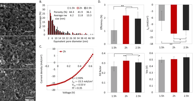
Biomineralization time strongly affects the morphology of the virus-templated titania film, and consequently the device performance. M13 bacteriophages are 6 nm in diameter by 880 nm in length, and can therefore create very fine titania nanostructures, as thin as 6 to 7 nm in diameter, after burning them off and sintering the crystallites. The reaction time in a 0.2 M TiCl4 solution
was varied between 1.5 and 2.5 hours, and the morphology, porosity and pore size distribution of the resulting titania network were compared. Figure 3A shows the surface morphology of the virus-templated titania films after 1.5, 2 and 2.5 hours of titania nucleation and subsequent annealing at 500 °C. It is readily observed that the porosity tends to decrease with increasing reaction time and that the diameter of nanowire-like features increase. The structure is highly porous after 1.5 h, and the pores begin to occlude after 2.5h in the reaction mixture. Therefore over time, the nanostructured and porous titania film become less porous and more planar. Image analysis revealed that the porosity decreased from 44.3% to 41.9% and 36.1% after 1.5, 2 and 2.5 hour reactions respectively (see Figure S5 for details). However, the pore size distribution is only slightly affected, with somewhat smaller pores being formed on average for shorter reaction times. A striking change in morphology between 1.5 and 2 hour reaction time is the diameter of nanowire-like features, which increase from an average of 6.2 nm to 11.8 nm.
The highest performing virus-templated device was obtained with a reaction time of 2 h (JV curve shown in Figure 3C). Therefore, the increase in nanowire diameter appears to have strongly affected the efficiency of the device and significantly increased the short-circuit current density, as observed in Figure 3D (see also Table 1). The average short-circuit current density and power conversion efficiency increased by about 2-fold in the devices biomineralized for 2 h compared to those biomineralized for only 1.5 h. The fill factor also increased from 1.5 to 2 h,
indicating that thicker nanowires decrease the series resistances by improving the electron conductivity through the titania mesh. The thicker nanowires could improve performance for two reasons: 1) it is less likely that there would be disconnects between neighboring titania crystallites, which would provide more direct pathways for electron collection, and 2) the larger titania crystallites comprising thicker nanowires would reduce the number of grain boundaries photogenerated electrons must travel through before collection at the electrode. Both reasons would minimize the interaction of electrons with grain boundaries, which would reduce the likelihood of non-radiative recombination occurring at defects at the titania surface and result in higher current generation and lower series resistances during operation. It is also expected that the samples mineralized for 1.5 h would have an increased variability between devices as the probability of electrical disconnects occurring along the mesh increases when less titania is allowed to nucleate along the biotemplate. The virus films biomineralized for 2.5 h hours also perform better than the ones reacted for 1.5 h, but the short-circuit current decreases compared to the 2 h biomineralization, likely due to the decrease in titania film porosity, which not only provides less pore volume for QDs to fill but also diminishes their ability to infiltrate into them. In summary, we found that the biomineralization time has a strong effect on device performance and that increasing time to an optimum of 2 h increases both the short-circuit current and the fill factor. For longer times, the efficiency might continue to plateau or decrease due to pore occlusion and flattening of the titania surface. These findings demonstrate that fine tuning the morphology of the titania-PbS layer is critical.
Figure 3. The biomineralization reaction time allows for tuning the feature size and porosity in
based devices, which affect device performance. A. Surface morphology of the virus-templated titania film captured by SEM, as a function of reaction time in TiCl4 (1.5, 2 and 2.5 h). B. Pore size distribution, porosity and average nanowire (nw) size for the different reaction times. Values were determined using image analysis. C. JV curve for device with best performance with a 2 h reaction time. D. Average and maximum device performance parameters as a function of the reaction time. Error bars represent standard deviation. Paired t-tests were performed and the statistically significant differences between pairs of results are shown by * for a p-value < 0.05 and ** for a p-value < 0.005. Exact values are reported in Table 1.
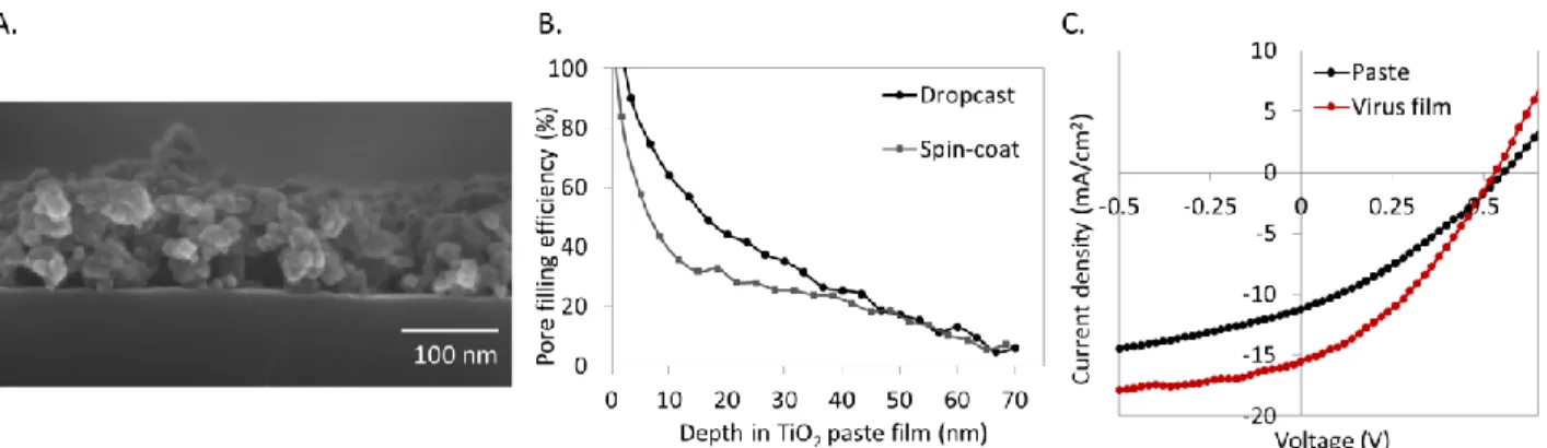
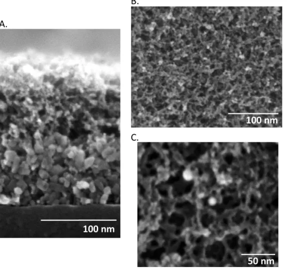
In order to demonstrate the advantages of using M13 bacteriophages as a scaffold to construct a continuous and porous titania matrix, our optimized virus-templated device was compared to an analogous device built using a titania nanoparticle paste. A titania paste was prepared using the same TiCl4 precursor at 0.2 M in water and collecting the particles formed after
a 2 h hydrolysis reaction (as opposed to using commercially available titania paste that may differ in surface chemistry, solvent and particle size from the titania nucleated on virus-templated films).
The particles were resuspended in a mixture of terpineol containing ethyl cellulose, which acts as a sacrificial polymer to introduce porosity within the film, and the final titania paste was spin-coated onto a silicon substrate to observe its morphology (Figure 4A). The resulting film has a porosity of 40%, which is comparable to that of the phage film biomineralized for 2 h (see Figure S6 for porosity estimation). However, as seen in Figure 4A, the nanoparticles are randomly oriented and particle size is polydisperse. When the phage film is immersed into a TiCl4 solution,
only the crystallites nucleated on the surface of the viruses remain in the film and create the uniform and organized networks of nanowires observed in Figures 1 and 3. In contrast, the paste is formed with all nanoparticles synthesized in solution during TiCl4 hydrolysis, and cannot be
easily purified to exclude larger aggregates that would roughen the final film or disorganize in an organized manner. Although the PbS infiltration profiles measured by XPS depth profiling follow a trend similar to the one observed for the virus films (Figure 4B), the short-circuit current density in the paste device was found to be almost 1.5 times lower than the virus-templated device, as shown in Figure 4C, and on average the performance of the optimized virus-template was two times higher than the paste control (see Table 1). This suggests that organizing titania nanoparticles into an interconnected network of nanowires allows for charges to be transported more efficiently than in a randomly distributed nanoparticle paste film. A nanoporous film composed of sintered nanoparticles likely provides a more circuitous route to electron collection, as is illustrated in Scheme 1, than the nanowire network, which would increase the likelihood of non-radiative recombination, reduce the collected photocurrent, and increase the device’s series resistance. Furthermore, the polydispersity of titania nanoparticles in the paste leads to rougher films, which likely contributes to the greater variability in performance observed for this device type.
Figure 4. Randomly organized TiO2 nanoparticles prepared from the same TiCl4 precursor result
in devices with a lower efficiency. A. Cross-sectional morphology of a TiCl4-based TiO2 paste
after annealing. The paste was spun at 2000 rpm onto a silicon substrate. B. PbS QD infiltration profile by dropcasting or spin-coating into the TiO2 paste film, resembling the infiltration profile
in a virus-templated TiO2 film. A depth of 0 nm corresponds to the interface between the top PbS
layer and the TiO2-PbS composite film. C. Comparison between the JV curve of a virus-templated
TiO2 film and a randomly organized nanoparticle film.
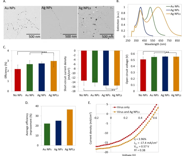
In addition to improving charge collection via the morphology of the nanoporous titania film, the performance of the solar cells was further improved by enhancing their ability to harvest light with metal nanoparticles (NPs), which concentrate light in the near-field via localized surface plasmon resonance (LSPR). This second approach to device improvement leverages the ability of the M13 bacteriophage to be genetically programmed to exhibit affinity for noble metals, which allows silver and gold nanoparticles to be complexed onto the viruses while in aqueous solution. The complexation process spaces the nanoparticles fairly evenly along the bacteriophages, which avoids aggregation and allows the characteristic absorption peaks of plasmonic particles to be preserved. TEM images of viruses complexed with spherical gold nanoparticles (Au NPs), spherical silver nanoparticles (Ag NPs), and silver triangular nanoplates (Ag NPLs) are shown in Figure 5A. As discussed in our previous report22, the act of binding to the virus causes the
aqueous colloids due to the presence of the virus proteins in the medium directly surrounding the NPs. Figure 5B presents the absorption spectra of all three NP-virus complexes in solution and clearly shows the characteristic dipole peak positions of Au NP at 520 nm, Ag NP at 400 nm, and both the dipole and quadrupole peaks of Ag NPLs at 620 and 400 nm, respectively.
Using our previously reported LbL-assembly process22, Au NPs, Ag NPs, and Ag NPLs
were evenly distributed throughout the nanoporous virus films without aggregation with a loading of approximately 0.1 NPs per virus (see Figure S7 for effect of NP concentration on device performance) and subsequently coated with a thin film of titania during the biomineralization process. These plasmonic nanoporous titania films were then used as the n-type component of the heterojunction QD solar cells. All types of nanoparticles improved the overall power conversion efficiency of the titania-PbS devices with the Ag NPLs producing the largest photocurrent enhancement (Figure 5C). The short-circuit current was enhanced in the presence of each nanoparticle type, with statistically significant improvement occurring with Ag NPs and Ag NPLs. In addition, the open circuit voltage (VOC) increased by approximately 50 mV (See Supporting
Information, and Figures S18 and S19) and the parasitic resistances improved (See Table S4) when adding any type of metal nanoparticle to the devices. As discussed further in the supporting information, the improvement in VOC is attributed to a natural increase that results from the
plasmonic NPs generating a higher photocurrent through LSPR. Likewise, the slight improvement in resistances could be attributed to either local changes in morphology or titania crystallite quality around the nanoparticles that improve charge transport. The improvement in power conversion efficiency (PCE) caused by the metal nanoparticles in the virus-templated devices was calculated to be 22.2% for Au NPs, 25.1% for Ag NPs, and 36.5% for Ag NPLs on average (Figure 5D and
Table 1). The top performing Ag NPL device reached a PCE close to 4%, and its JV curve is compared to a virus-templated device without plasmonic nanoparticles in Figure 5E.
Figure 5. The incorporation of noble metal nanoparticles improves the efficiency of the
virus-templated titania-PbS QD depleted bulk heterojunction devices. TEM images (A) and corresponding absorption spectra (B) for virus-nanoparticle complexes that were incorporated into the films. C. Comparison of power conversion efficiency, short-circuit current density and open circuit voltage for devices with naked virus, or for viruses complexed with Au NPs, Ag NPs or Ag NPLs. Paired t-tests were performed and the statistically significant differences between pairs of results are shown by ** for a p-value < 0.005 and *** for a p-value < 0.0005. D. Average percentage improvement in efficiency with addition of metal nanoparticles. E. Comparison of the JV curves for the best device with and without metal nanoparticles. Overall, the nanoparticle device with the highest efficiency contained Ag NPLs. Exact values are reported in Table 1.
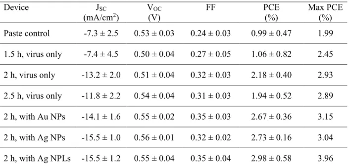
Table 1. Solar cell performance parameters for TiO2 NP paste control device, virus-based device,
and plasmonic virus-based devices. Average values and standard deviations are presented for each parameter, as well as the maximum power conversion efficiency (PCE) for each type of device. The averages presented are based on at least 10 to 20 devices of each type.
Device JSC
(mA/cm2) V(V) OC FF PCE (%) Max PCE (%)
Paste control -7.3 ± 2.5 0.53 ± 0.03 0.24 ± 0.03 0.99 ± 0.47 1.99 1.5 h, virus only -7.4 ± 4.5 0.50 ± 0.04 0.27 ± 0.05 1.06 ± 0.82 2.45 2 h, virus only -13.2 ± 2.0 0.51 ± 0.04 0.32 ± 0.03 2.18 ± 0.40 2.93 2.5 h, virus only -11.8 ± 2.2 0.54 ± 0.04 0.31 ± 0.03 1.94 ± 0.52 2.89 2 h, with Au NPs -14.1 ± 1.6 0.55 ± 0.02 0.35 ± 0.03 2.67 ± 0.36 3.15 2 h, with Ag NPs -15.5 ± 1.0 0.56 ± 0.01 0.32 ± 0.02 2.73 ± 0.16 3.04 2 h, with Ag NPLs -15.5 ± 1.2 0.55 ± 0.04 0.35 ± 0.04 2.98 ± 0.58 3.96
It must be noted that significantly higher device performances can be obtained for devices with areas five times smaller (See Figure S10 for details). The higher average performance observed for smaller area devices is likely due to the reduced probability of defects in the film, which significantly increases the short-circuit current and the fill factor for a constant open circuit voltage. We believe, however, that reporting values for larger areas are more valuable since the ultimate goal is to produce large area photovoltaic devices and panels.
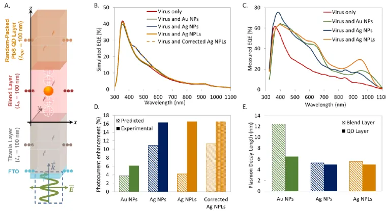
The effect of each nanoparticle type on the ability of the devices to harvest light was computationally predicted prior to device fabrication by combining effective medium theory with finite-difference time-domain (FDTD) calculations. As illustrated in Figure 6A, the simulation geometry follows the approximate dimensions of an actual device cross-section, which consists of stacked slabs of homogeneous materials starting with an FTO base layer, a 100 nm thick compact
NP, a 100 nm thick layer of random-packed PbS QDs, and a 25 nm thick MoO3 layer on top.
Periodic boundary conditions were placed on both the x and y lateral directions in order to simulate a unit cell of the solar cell slab, which allowed any light scattered out of the sides of the simulated domain to be reabsorbed elsewhere in the unit cell. The extent of the unit cell in the x and y lateral directions was set to 60 nm, which is the estimated approximate distance between nanoparticles in the virus-templated titania film. Finally, the unit cell was illuminated through the FTO layer by a plane wave with wavelengths ranging from 200 to 1200 nm and a three-dimensional power monitor was placed throughout the unit cell to sample the power density of light absorbed at each node in the mesh for each simulated wavelength. Because a nanoparticle can be located at any vertical position within the blend layer, five separate FDTD simulations were performed for each nanoparticle type, each with the nanoparticle center positioned at a different elevation (10, 30, 50, 70, and 90 nm into the blend layer). A sixth simulation was performed with the nanoparticle positioned 10 nm into the QD film layer to account for roughness of the virus film, which would cause a NP located near the top of the blend layer to be surrounded by a higher fraction of QDs. The ensemble average over all six configurations was taken during the analysis to approximate the effect of inherent randomness of homogeneously distributed NPs throughout the thickness of the virus-templated film has upon light absorption.
Aside from the geometry of the model, developing a realistic description of the complex dielectric function of the photoactive materials in the optical model is critical to capturing how light is absorbed as it propagates through the device architecture and how far the near-field generated by the plasmonic NP extends into the active regions. The complex dielectric function of the compact titania, titania-PbS blend layer, and packed PbS QD layers were calculated using effective medium theory in conjunction with values adjusted from previous reports for anatase thin
films39 and PbS quantum dots40 (see supporting information for details). When a monodisperse
solution of PbS QDs is deposited onto a planar film, the nanospheres will pack into a porous layer with voids existing between them. Because the size of a quantum dot is substantially smaller than the wavelength of light, light cannot distinguish between an individual particle and the air in the voids, rather it perceives an effective dielectric medium that is a blending of the material properties of the two components. Therefore, the dielectric function of a randomly-packed PbS QD layer deposited on top of the nanoporous titania film was calculated using the Maxwell-Garnett effective medium model. Similarly, when the pores of the virus-templated titania film are infiltrated with the PbS QDs, the resulting film is a blend of anatase titania, PbS, and air void-space, which was modelled using the Bruggemann model as an effective homogeneous medium with a dielectric function that depends on the porosity of the virus-templated film (see supporting information for details). For simplicity, it was assumed that the PbS QDs are homogeneously distributed throughout both the blend and QD film layers with a volume fraction of 56% in the spin-coated QD layer and 15% in the blend layer. A value of 56% in the QD film corresponds to a loose random-packing,35 which is considered more appropriate than the 74% value associated with
regular close-packed beds because spin-coated films of QDs have been shown to be less-regularly packed with packing densities around 50%.41 Likewise, a 15% PbS volume fraction in the blend
layer was calculated by averaging the infiltration data of spin-coated PbS QDs into the virus film reported in Figure 1D over the film thickness.
By illuminating the simulated device with a flat irradiance across all wavelengths and integrating the absorbed power density over the spatial extent of the photoactive regions of the device, i.e. the titania-PbS QD blend layer and the random-packed QD layer, we predicted how
absorption efficiency, 𝜂𝑎. However, the performance of solar cells depends not only on its ability
to absorb photons, but also on how well those photons can be converted into charges and how efficiently those charges can be collected at the electrodes. Therefore, some basic assumptions were applied to build a simple model for charge collection efficiency, 𝜂𝑐, mainly: (1) it is assumed
that all of the absorbed power in the blend layer can be converted to charges and collected because it is within the depletion region. Secondly, (2) it is assumed that carriers generated deeper in the close-packed QD layer are less likely to migrate to the titania in the blend layer before recombination occurs than those generated closer to the blend layer interface. Therefore, an exponential decay envelop with a decay length of 30 nm42 was applied to the absorbed power
density values in the quasi-neutral region in order to capture the fact that carriers generated closer to the blend layer are more likely to diffuse to the depletion region for collection and contribute to the device photocurrent:
𝜂𝑐={ 1, 0 ≤ 𝑧 ≤ 𝐿𝑏
𝑒−(𝑧−𝐿𝑏)/𝐿𝑑, 𝐿𝑏< 𝑧 ≤ 𝐿𝑏+ 𝐿𝑄𝐷
where 𝐿𝑏 is the thickness of the depletion region, 𝐿𝑄𝐷 is the thickness of the quasi-neutral region, and 𝐿𝑑 is the electron decay length in PbS QD films.
The product of the absorption and collection efficiencies provides an estimate of the external quantum efficiency (EQE) spectra for each device, which quantifies how efficiently incident photons of a given wavelength are converted into collected charges. Figure 6B and C, respectively, show the computed and measured EQE spectra for devices loaded with each type of silver plasmonic particle. The overall shape of the simulated and measured EQE spectra for the devices without nanoparticles are remarkably similar, with a main peak arising around 375 nm followed by a slowly decaying profile at higher wavelengths. The simulations predict a clear
plasmon-induced performance enhancement starting around 400 nm for Ag NPs and 525 nm for Au NPs, which is in good agreement with the observed regions of power enhancement in the actual devices..
In contrast, the predictions for Ag NPLs dramatically underestimate the observed performance increase in devices. This is likely due to the Ag NPLs changing shape and size during the device fabrication process. First, monitoring their shape and absorption spectrum during LbL assembly indicated an evolution from triangular nanoplates to circular nanodiscs and nanoparticles (Figure S8). Second, it is expected that the nanoplates originally incorporated into the films transformed into a polydisperse population of nanospheres during the device annealing process performed to crystallize the titania network. It has been observed that colloidal nanoplate solutions tend to stack upon one another when dried on TEM grids (Figure S9). It is possible that during the LbL process used to build the virus films, free nanoplates could stack upon those that have been already bound to the virus, which later convert into various sizes of silver nanospheres during annealing. A polydisperse nanosphere population would result in a broader enhancement wavelength range consistent with the wide region of enhancement demonstrated by the EQE measurement shown in Figure 6C. This hypothesis was also investigated computationally by running simulations using Ag nanospheres whose volume is conserved from stacks of 1, 2, or 3 Ag NPLs. Averaging the results produces a corrected simulated EQE spectrum that is much closer to the measurements made for devices originally made using Ag NPLs.
Although a metal nanoparticle absorbs light, the power contained within its interior does not contribute to the photogeneration of carriers and is generally lost as heat. Only light concentrated in the NP’s near-field that extends into the surrounding active layer will contribute
have otherwise been filled with a blend of titania and QDs in its absence, therefore the near-field generated by the NP must overcome this loss. Thus, enhancement is only expected to occur at wavelengths where LSPR occurs and performance is expected to be slightly reduced at off-resonant wavelengths because less QDs are physically present in the model to absorb photons at these energies. This is the reason why the simulated EQE spectra of the plasmonic devices are slightly reduced from the devices without NPs at short wavelengths. Discrepancies between the predicted and measured EQE spectra are likely due to local spatial variations in the effective complex dielectric function of the media in the device arising from (1) PbS QDs not being homogeneously distributed throughout the actual blend layer thickness, and (2) roughness at the interfaces between layers. In actuality, a QD concentration gradient exists as is shown in Figure 1D, which is not explicitly considered by the model. Similarly, roughness at the interface between the blend layer and the random-packed QD layer would cause a nearby NP to sense an effective medium comprised of a higher fraction of PbS than a NP buried within the blend layer. The result of both cases is to broaden the wavelength range of plasmon enhancement as metal nanoparticles located at different positions in the actual active layers would experience different effective local dielectric functions of the surrounding medium, thereby producing LSPR peaks at different wavelength positions and broadening the spectra of the ensemble average. Since the idealized model presented herein is sufficient to capture the observed trends in the measurements, any further modeling of local variations in geometry and material properties is considered to be beyond the scope of this report.
The presented model clearly demonstrates for the Ag nanosphere case that the wavelengths between 400 and 600 nm where significant EQE enhancement occurs can be explained by LSPR acting to concentrate light in the near-field region surrounding the noble metal nanoparticles. This
increases the photon flux incident on QDs located within the near-field, thereby increasing their rates of charge carrier generation. The ability of a plasmonic NP to enhance photocurrent generation in a solar cell can be quantified by defining an enhancement factor, EF, which compares the predicted short circuit current density (Jsc) resulting in the unit cell geometry that contains a
NP to the prediction of the Jsc in the same unit cell without the NP:
𝐸𝐹 = 𝐽𝑠𝑐 from Unit Cell with a NP 𝐽𝑠𝑐 from Unit Cell without a NP
= ∫ (∫𝑉𝑜𝑙𝑢𝑚𝑒 𝑖𝑛 𝑎𝑐𝑡𝑖𝑣𝑒 𝑝𝑎𝑏𝑠(𝑥⃑, 𝜆)𝜂𝑐(𝑧)𝑑3𝑥 𝑟𝑒𝑔𝑖𝑜𝑛 𝑜𝑢𝑡𝑖𝑠𝑑𝑒 𝑁𝑃 )ℎ𝑐𝜆 𝑀𝐴𝑀1.5(𝜆)𝑑𝜆 ∫ (∫𝑉𝑜𝑙𝑢𝑚𝑒 𝑖𝑛 𝑝𝑎𝑏𝑠𝑜 (𝑥⃑, 𝜆)𝜂𝑐(𝑧)𝑑3𝑥 𝑎𝑐𝑡𝑖𝑣𝑒 𝑟𝑒𝑔𝑖𝑜𝑛 )ℎ𝑐𝜆 𝑀𝐴𝑀1.5(𝜆)𝑑𝜆
where 𝑝𝑎𝑏𝑠 is the absorption efficiency density as a function of position and wavelength for a unit
cell containing a plasmonic NP, 𝑝𝑎𝑏𝑠𝑜 is the absorption efficiency density as a function of position
and wavelength for the same unit cell without a NP, 𝑀𝐴𝑀1.5 is the solar irradiance for the AM1.5 global solar spectrum, ℎ is Planck’s constant, 𝑐 is the speed of light, and 𝜂𝑐 is the carrier collection
probability. The enhancement factor can be directly compared to the ratio of the short circuit current density, 𝐽𝑠𝑐, for a unit cell with NPs to that without, 𝐽𝑠𝑐𝑁𝑃/𝐽
𝑠𝑐𝑛𝑜𝑁𝑃, which is presented in
Figure 6D. The measured devices demonstrate higher photocurrent enhancement than the simulations predicted with the measured enhancement being 6.2%, 16.3%, and 16.5% for solar cells with Au NPs, Ag NPs, and Ag NPLs respectively, whereas simulations predicted 3.8, 10.9, and 4.2%. When the photocurrent is calculated for a polydisperse population of Ag NPs that have been transformed from Ag NPLs, the predicted enhancement rises to 11.3%. Although the predictions were lower than observed photocurrent enhancement, the trend is clearly captured. It is worth noting that devices with Ag NPs in both the simulated and measured devices produce a photocurrent enhancement roughly three times larger than devices with Au NPs.
The model presented can only explicitly account for enhancement of the device photocurrent and cannot account for any differences in parasitic resistances and the fill factor between devices, which fortunately do not change significantly between virus-based solar cells with and without plasmonics NPs. However, the increase in Voc that is observed in plasmonic
devices likely arises directly from their corresponding increase in photocurrent due to enhanced light harvesting. The standard diode equation model for solar cells couples the current and voltage together; therefore, the open circuit voltage of a device will change if it can output a higher photocurrent. By fitting each of the measured JV curves for virus-based devices with and without plasmonic NPs to the standard diode equation for solar cells, it was revealed that the Voc increase
observed for the device with Ag NPLs (Figure 5E) corresponds to the Voc predicted by the standard
solar cell model if the virus-based device without plasmonic NPs happened to experience an increase in photocurrent equal to that observed in the virus-based device with Ag NPLs (see supporting information for details). Therefore, the effect of LSPR conveniently causes both the Jsc
and Voc to rise in the plasmonic devices, causing the observed overall enhancement in PCE to be
even higher.
Figure 6. FDTD simulations we used to rationally design and predict the plasmon enhancement
in devices containing metal nanoparticles. A. Geometry of simulations. B. Predicted and C. Measured EQE spectra for devices containing Au NPs, Ag NPs or Ag NPLs, compared to virus-only devices. Experimental EQE curves with metal nanoparticles were adjusted based on measured average short-circuit current values for each type of device. D. Predicted and measured photocurrent enhancement compared to virus-templated devices without nanoparticles. E. Predicted plasmon decay length for different nanoparticles embedded in the blend and random-packed QD layers.
Lastly, as demonstrated in Figure 6E, blending the PbS QDs with the titania nanoporous network provides an effective medium that allows the near-field surrounding the metal NPs to propagate further into the blend layer than they would if incorporated into the random-packed QD layer. This is a direct result of the effective complex index of the blend layer being lower than the random-packed QD film by virtue of its lower volume fraction of PbS. This is useful from a practical standpoint because the larger the extent of the near-field, the greater the chance a PbS QD can experience a higher photon-flux and exist in a defect-free region that can efficiently
CONCLUSIONS
In conclusion, we demonstrate that the high aspect ratio M13 bacteriophage can serve as a template to form nanocomposites that are suitable for thin film solar devices. However, in order to make an effective device, many processing parameters had to be optimized to maximize device efficiency. First, we found that a short chain PEI polymer was the optimal surface functionalization molecule to adsorb the bacteriophages to the titania base layer because it could form a very thin layer that was minimally insulating. Second, we showed that the biomineralization time could be optimized to allow for the thickening of the nanowire-features while maintaining the film porosity. Third, the best method for infiltrating PbS QDs into the pores was found to be a combination of dropcasting and spincoating as determined by XPS depth profiling measurements. Although the pores are on average 10 nm in size, the 2.9 nm diameter QDs could substantially infiltrate throughout the virus-templated titania film. Last, we determined the optimal amount of plasmonic nanoparticles that would maximize the enhancement in photocurrent.
Compared to a randomly organized nanoparticle paste control, we confirmed that the virus-based titania morphology had a significant impact on the photocurrent of the device. A two-fold improvement in device efficiency suggests that the high aspect ratio of the virus improves charge transport within the active layer. Devices with AuNP, Ag NPs, and Ag NPLs incorporated into the active layers of solar cells showed an improved light harvesting ability in the EQE spectra near the expected LSPR peak positions and subsequent enhancement in the Jsc, Voc, and PCE, with PCE
enhancements reaching 36.5% over based control devices with Ag NPLs. How the virus-templated nanoporous morphology affected the propagation of light through the solar cells was numerically computed by modelling the nanostructured device layers with effective medium
theory and using the FDTD method to calculate how power is absorbed throughout the devices. The main features of the predicted EQE spectra and photocurrent enhancement for devices with Au NPs, Ag NPs, and Ag NPLs were in good agreement with the trends observed in measurements, indicating that LSPR is primarily responsible for the observed improvements in light harvesting and photocurrent in plasmon-enabled solar cells. Furthermore, the simulations indicate that generating a blended titania-PbS active layer produces a larger near-field compared with the random-packed QD layer, thereby increasing the chance that light concentration occurs at a point without structural or electronic defects that impair charge generation and transport. Therefore, the virus-templated geometry not only improves the ability of the device to collect and transport charges from the bulk of the device, but also the practical ability of plasmons to enhance light harvesting.
Finally, it is expected that combining our plasmon-enhanced virus-based titania nanotemplate with new ligand molecules and interface engineering techniques that are currently being developed could further improve the efficiency of titania-quantum dot photovoltaic devices. Furthermore, our strategy is intended to be a platform that could be applied to other solution-processable thin film solar systems such as hybrid organic-inorganic solar cells and photocatalytic platforms. Our optimized procedures for assembling and mineralizing the nanoporous virus-based film could be extendable to other biotemplates and find use in any system that interfaces electronic components with biological materials.
ASSOCIATED CONTENT
Supporting Information. Supplementary figures and method details can be found in supporting
AUTHOR INFORMATION
Corresponding Author
Angela M. Belcher (Belcher@mit.edu) and Paula T. Hammond (Hammond@mit.edu)
Author Contributions
The manuscript was written through contributions of all authors. All authors have given approval to the final version of the manuscript. N.-M.D.C., M.T.K., A.M.B. and P.T.H. conceived the idea. N.-M.D.C. and M.T.K. designed the experiments and analyzed the data. N.-M.D.C assembled and characterized the thin films, fabricated and tested the solar cells. M.T.K.
synthesized the metal nanoparticles. M.T.K. and N.X.F. performed and analyzed the simulations. V.J.C. and P-Y.C. assisted with substrate and thin film preparation. K.J.H, M.C.W. and W.A.T. synthesized and characterized the PbS quantum dots. S.E.K. prepared a cross-sectional TEM sample, and D.S.Y. performed elemental mapping of the sample.
ACKNOWLEDGMENT
N.-M.D.C, M.T.K. and P.-Y.C. acknowledge support from Eni-MIT Energy Fellowships through the MIT Energy Initiative Program. This work made use of the MIT MRSEC Shared Experimental Facilities supported by the National Science Foundation under award number DMR-0819762. The authors wish to express their appreciation to the Institute for Soldier Nanotechnologies at MIT, supported by the Army Research Office and Army Research Laboratories, whose facilities and/or equipment were used to conduct the research reported in this paper. We thank the MIT Koch Institute Swanson Biotechnology Center, which is supported by the Koch Institute Core Grant P30-CA14051 from the NCI, for the use of facilities, and specifically the Peterson (1957) Nanotechnology Core Facility. We would also like to thank Patrick Brown and Joel Jean for helpful discussions and the Organic and Nanostructured Electronics laboratory operated by Prof.
Vladimir Bulović at MIT for use of their facilities for thermal evaporation and device characterization. N.-M.D.C. gratefully acknowledges the Postgraduate Scholarship support from the Natural Sciences and Engineering Research Council of Canada (NSERC). M.C.W. was supported by a National Science Foundation Graduate Research Fellowship under Grant No. 1122374.
ABBREVIATIONS
APTMES, (3-aminopropyl)trimethoxysilane; EDC, 1-ethyl-3-(-3-dimethylaminopropyl)
carbodiimide; FDTD, finite-difference time-domain; FTO, fluorine-doped tin oxide; LbL, layer-by-layer; LSPR, Localized surface plasmon resonance; MPA, mercaptopropionic acid; NPs, nanoparticles; NPLs, nanoplates; PAA, polyacrylic acid; PAH, polyallylamine hydrochloride; PEI, polyethyleneimine; QDs, quantum dots; SEM, scanning electron microscopy; TEM, transmission electron microscopy; XPS, X-ray photoelectron spectroscopy.
REFERENCES
1. Lou, S. J.; Szarko, J. M.; Xu, T.; Yu, L.; Marks, T. J.; Chen, L. X., Effects of Additives on the Morphology of Solution Phase Aggregates Formed by Active Layer Components of High-Efficiency Organic Solar Cells. Journal of the American Chemical Society 2011, 133 (51), 20661-20663.
2. Maturová, K.; van Bavel, S. S.; Wienk, M. M.; Janssen, R. A. J.; Kemerink, M., Description of the Morphology Dependent Charge Transport and Performance of
Polymer:Fullerene Bulk Heterojunction Solar Cells. Advanced Functional Materials 2011, 21 (2), 261-269.
3. Oh, J.; Yuan, H.-C.; Branz, H. M., An 18.2%-efficient black-silicon solar cell achieved through control of carrier recombination in nanostructures. Nat Nano 2012, 7 (11), 743-748. 4. Oosterhout, S. D.; Wienk, M. M.; van Bavel, S. S.; Thiedmann, R.; Jan Anton Koster, L.; Gilot, J.; Loos, J.; Schmidt, V.; Janssen, R. A. J., The effect of three-dimensional morphology on the efficiency of hybrid polymer solar cells. Nat Mater 2009, 8 (10), 818-824.
5. Saunders, B. R., Hybrid polymer/nanoparticle solar cells: Preparation, principles and challenges. Journal of Colloid and Interface Science 2012, 369 (1), 1-15.
6. Jean, J.; Chang, S.; Brown, P. R.; Cheng, J. J.; Rekemeyer, P. H.; Bawendi, M. G.; Gradečak, S.; Bulović, V., ZnO Nanowire Arrays for Enhanced Photocurrent in PbS Quantum Dot Solar Cells. Advanced Materials 2013, 25 (20), 2790-2796.
7. Kramer, I. J.; Zhitomirsky, D.; Bass, J. D.; Rice, P. M.; Topuria, T.; Krupp, L.; Thon, S. M.; Ip, A. H.; Debnath, R.; Kim, H.-C.; Sargent, E. H., Ordered Nanopillar Structured Electrodes for Depleted Bulk Heterojunction Colloidal Quantum Dot Solar Cells. Advanced Materials 2012,
24 (17), 2315-2319.
8. Lan, X.; Bai, J.; Masala, S.; Thon, S. M.; Ren, Y.; Kramer, I. J.; Hoogland, S.; Simchi, A.; Koleilat, G. I.; Paz-Soldan, D.; Ning, Z.; Labelle, A. J.; Kim, J. Y.; Jabbour, G.; Sargent, E. H., Self-assembled, nanowire network electrodes for depleted bulk heterojunction solar cells.
Advanced Materials 2013, 25 (12), 1769-1773.
9. Etgar, L.; Moehl, T.; Gabriel, S.; Hickey, S. G.; Eychmüller, A.; Grätzel, M., Light energy conversion by mesoscopic PbS quantum dots/TiO 2 heterojunction solar cells. ACS Nano
2012, 6 (4), 3092-3099.
10. Rath, A. K.; Bernechea, M.; Martinez, L.; de Arquer, F. P. G.; Osmond, J.; Konstantatos, G., Solution-processed inorganic bulk nano-heterojunctions and their application to solar cells.
Nat Photon 2012, 6 (8), 529-534.
11. Wang, K. X.; Yu, Z.; Liu, V.; Cui, Y.; Fan, S., Absorption Enhancement in Ultrathin Crystalline Silicon Solar Cells with Antireflection and Light-Trapping Nanocone Gratings. Nano
Letters 2012, 12 (3), 1616-1619.
12. Battaglia, C.; Escarre, J.; Soderstrom, K.; Charriere, M.; Despeisse, M.; Haug, F.-J.; Ballif, C., Nanomoulding of transparent zinc oxide electrodes for efficient light trapping in solar cells. Nat Photon 2011, 5 (9), 535-538.
13. Atwater, H. A.; Polman, A., Plasmonics for improved photovoltaic devices. Nat Mater
2010, 9 (3), 205-213.
14. Choi, H.; Lee, J.-P.; Ko, S.-J.; Jung, J.-W.; Park, H.; Yoo, S.; Park, O.; Jeong, J.-R.; Park, S.; Kim, J. Y., Multipositional Silica-Coated Silver Nanoparticles for High-Performance
Polymer Solar Cells. Nano Letters 2013, 13 (5), 2204-2208.
15. Dang, X.; Qi, J.; Klug, M. T.; Chen, P.-Y.; Yun, D. S.; Fang, N. X.; Hammond, P. T.; Belcher, A. M., Tunable Localized Surface Plasmon-Enabled Broadband Light-Harvesting Enhancement for High-Efficiency Panchromatic Dye-Sensitized Solar Cells. Nano Letters 2013,
13 (2), 637-642.
16. Paz-Soldan, D.; Lee, A.; Thon, S. M.; Adachi, M. M.; Dong, H.; Maraghechi, P.; Yuan, M.; Labelle, A. J.; Hoogland, S.; Liu, K.; Kumacheva, E.; Sargent, E. H., Jointly Tuned
Plasmonic–Excitonic Photovoltaics Using Nanoshells. Nano Letters 2013, 13 (4), 1502-1508. 17. Betancur, R.; Romero-Gomez, P.; Martinez-Otero, A.; Elias, X.; Maymo, M.; Martorell, J., Transparent polymer solar cells employing a layered light-trapping architecture. Nat Photon
2013, 7 (12), 995-1000.
18. Dang, X.; Yi, H.; Ham, M.-H.; Qi, J.; Yun, D. S.; Ladewski, R.; Strano, M. S.; Hammond, P. T.; Belcher, A. M., Virus-templated self-assembled single-walled carbon
nanotubes for highly efficient electron collection in photovoltaic devices. Nat Nano 2011, 6 (6), 377-384.
19. Oh, D.; Dang, X.; Yi, H.; Allen, M. A.; Xu, K.; Lee, Y. J.; Belcher, A. M., Graphene Sheets Stabilized on Genetically Engineered M13 Viral Templates as Conducting Frameworks for Hybrid Energy-Storage Materials. Small 2012, 8 (7), 1006-1011.
20. Nam, K. T.; Kim, D.-W.; Yoo, P. J.; Chiang, C.-Y.; Meethong, N.; Hammond, P. T.; Chiang, Y.-M.; Belcher, A. M., Virus-Enabled Synthesis and Assembly of Nanowires for Lithium Ion Battery Electrodes. Science 2006, 312 (5775), 885-888.