Design and Implementation of Three-Dimensional
Logic Structures
by
Shamik Das
Submitted to the Department of Electrical Engineering and Computer
Science
in Partial Fulfillment of the Requirements for the Degrees of
Bachelor of Science in Electrical Science and Engineering
and
Master of Engineering in Electrical Engineering and Computer Science
at the
MASSACHUSETTS INSTITUTE OF TECHNOLOGY
June 2000
©
Shamik Das, MM. All rights reserved.
The author hereby grants to MIT permission to reproduce and
distribute publicly paper and electronic copies of this thesis document
in whole or in part, and to grant others the right to do so.
MASSACHUSETTS INSTITUTE OF TECHNOLOGY
JUL 2 7 2000
Author ...
...
.LIBRARIES
Department of Electrical Engineering and Computer Science
May 22, 2000
C ertified by ... ...
...
SV
Joseph Jacobson
Associate-Professor, Media Arts and Sciences
-
:;jhis
S3ervisor
Accepted by...
. ...
Art hu+r
ni.t
Chairman, Department Committee on Graduate Students
Design and Implementation of Three-Dimensional Logic
Structures
by
Shamik Das
Submitted to the Department of Electrical Engineering and Computer Science on May 22, 2000, in Partial Fulfillment of the
Requirements for the Degrees of
Bachelor of Science in Electrical Science and Engineering and
Master of Engineering in Electrical Engineering and Computer Science
Abstract
In this thesis, a computer-aided-design (CAD) system is developed that assists in the design of novel three-dimensional integrated circuits. The software tools allow for the specification of a multilayer transistor circuit by means that are readily accessible to those familiar with two-dimensional CMOS VLSI design. This software system provides desirable features such as SPICE circuit extraction and the ability to produce the design formats necessary for automated fabrication (e.g. mask specifications for lithography or Gerber data for inkjet printing). Finally, in this thesis, the software tools are used to design a ring oscillator, a 3-D static RAM, and a 3-D cellular automata machine.
Thesis Supervisor: Joseph Jacobson
Acknowledgments
I am grateful to many people for their support in the development of this thesis. My thesis advisor, Joe Jacobson, deserves thanks for his guidance and motivation, as well as for many helpful discussions about the research. Babak Nivi, Colin Bulthaup, and Eric Wilhelm were instrumental in fabricating test structures from the software-produced specifications. I also appreciate the many TFT discussions with Babak, Colin, and Brent Ridley, as these were important for shaping the form the circuit-design process was to take. Saul Griffith and Sawyer Fuller deserve thanks for their input on laser and inkjet patterning of functional materials.
In addition, this thesis would not have been completed without the support of many friends, brothers, and loved ones. I would especially like to thank my family - my parents, Dilip and Mala, and my sister, Alina - for their inspiration, direction, and support.
Contents
1 Introduction
1.1 Design of the Layout Software . . . . . 1.2 Implementation of Test Circuits . . . .
1.2.1 Ring Oscillator . . . . 1.2.2 Static Random-Access Memory 1.2.3 Cellular Automata Machine 2 FluidLayout - The Layout Software
2.1 Overall Considerations . . . . 2.2 Implementation . . . . 2.2.1 2-D Slice Manipulation . . . . . 2.2.2 Circuit Partitioniing . . . . 2.3 Circuit Verification . . . . 2.4 Circuit Fabrication . . . . 2.5 Design Walk-Through . . . . 3 Some Basic Transistor Circuits
3.1 Minimum Criteria for the Technology 3.2 Design of Basic Circuits . . . . 4 The Static Random-Access Memory
4.1 Background and Motivation . . . . . 4.2 SRAM operation . . . . 8 10 12 12 13 14 16 17 20 21 24 26 27 28 31 31 34 42 43 44 . . . . . . . . . . . . . . . .
4.3 Extensions to 3-D . . . . 46
4.4 Layout of a 3-D SRAM . . . . 51
5 The Cellular-Automata Machine 55 5.1 Background . . . . 55
5.1.1 Finite-State Machines . . . . 55
5.1.2 Cellular-Automata Machines . . . . 57
5.1.3 The Game of Life . . . . 59
5.2 Layout of a 3-D Game of Life . . . . 60
5.2.1 Game of Life Cell . . . . 60
5.2.2 Game of Life CAM Architecture . . . . 62
6 Conclusion 67 A FluidLayout User's Guide 69 A .1 O verview . . . . 69
A.2 Basic Layout . . . . 69
A.3 Higher-Level Functions . . . . 71
A.3.1 Node Labeling . . . . 71
A.3.2 Translation, Rotation, and Reflection . . . . 72
A.4 Circuit-Level Tools . . . . 74
A.4.1 Circuit Traversal . . . . 74
A.4.2 Cell Hierarchy Management . . . . 74
A.4.3 Magic Importation . . . . 75
A.4.4 Circuit Netlist Extraction . . . . 75
A.4.5 VLSI/MEMS Fabrication . . . . 75
A.5 Step-By-Step Design Walk-Through . . . . 78
List of Figures
2-1 CLayer object with embedded CRectangle objects. . . . . 22
2-2 Corner-stitched CRectangle object. . . . . 23
2-3 Area enumeration of CRectangle objects within a bounding rectangle. 24 2-4 Canonical technology used in FluidLayout. . . . . 26
2-5 Box-outlining is used to place materials in FluidLayout. . . . . 28
2-6 Complete NMOS pulldown path. . . . . 29
2-7 Placement of a metal2-+gate via results in a gate-+metal2 hint on the second layer. . . . . 29
2-8 The com plete inverter. . . . . 30
3-1 NM O S inverter. . . . . 32
3-2 NMOS inverter small-signal model about VM. . . . . 33
3-3 Layout of test devices. . . . . 35
3-4 3-D layout of a ring oscillator. The three inverters shown are stacked to form the 3-D layout. . . . . 36
3-5 Stamp pattern with spatially-separated material patterns. . . . . 39
3-6 Patterned gate for a NOR gate, SRAM cell, and ring oscillator. . . . 40
3-7 Patterned source/drain for a NOR gate, SRAM cell, and ring oscillator. 41 4-1 Six-transistor circuit for individual bit storage. . . . . 45
4-2 Eight-transistor circuit for use in 3-D SRAM. . . . . 47
4-3 Proper cell distribution improves aspect ratio and decreases bit-line length... ... 48
4-5 First and second layers of an eight-layer 3-D SRAM . . . . 52
4-6 6-T SRAM cell layout. . . . . 53
4-7 Word-line tri-stating. . . . . 53
4-8 Bit-line decoding using the word-line tri-state control signal. . . . . . 54
5-1 Finite state machine. . . . . 56
5-2 Turing machine. . . . . 57
5-3 Four cells of a cellular-automata machine. . . . . 58
5-4 Insertion sort bit-slice. . . . . 62
5-5 G am e of Life cell. . . . . 63
5-6 Clock distribution in the 3-D Game of Life architecture . . . . 64
5-7 Layer of a 3-D Game of Life architecture comprising a 4 x 4 array of cells. . . . . 6 6 A-1 FluidLayout screenshot. . . . . 70
A-2 The main FluidLayout toolbar. . . . . 71
A-3 Partial view showing node selection . . . . 72
A-4 Label dialog . . . . 73
A-5 Subcircuit rotation. . . . . 73
A-6 Cell hierarchy management toolbar. . . . . 74
A-7 Edit->Properties->Laser Setup ... ... 76
A-8 4 x 2 box used for the source of an NMOS transistor. . . . . 79
A-9 Completed source node of the NMOS transistor. . . . . 79
A-10 NMOS source and drain nodes. . . . . 79
A-11 Inverter source and drain nodes. . . . . 80
A-12 Complete inverter. . . . . 81
A-13 Window menu. . . . . 82
A-14 First-layer inverter with contact pads. . . . . 83
A-15 First-layer inverter with via stacks to the second layer. . . . . 84
A-16 Labeled first-layer inverter. . . . . 85
Chapter 1
Introduction
CMOS integrated circuits are traditionally fabricated on crystalline silicon wafers. Transistor structures are created on the surface of these wafers by implantation into the wafer and growth and deposition of material over the surface of the wafer. This fundamentally results in a two-dimensional circuit layout, as the transistors are con-fined to inhabit the boundary of the silicon substrate.
However, a number of advances in solid-state technology have made possible the development of more complicated three-dimensional transistor structures. All of these advances rely on the creation of two-dimensional circuit "layers" by stan-dard means, and then interconnecting these layers into a multi-layer structure. For example, the development of wafer-scale integration (WSI) allows for the creation of three-dimensional circuits by stacking wafers using a lift-off and bonding process [24]. Also, the advent of silicon-on-insulator (SOI) technology allows for a third dimension of circuitry by encapsulating an existing two-dimensional circuit with insulating ma-terial, planarizing this mama-terial, and placing the next layer of silicon on this insulator. A very promising path to multi-layer transistor circuits involves the use of solution-processed metals, semiconductors, and insulators. Transistors can be laid out by depositing the appropriate solutions onto an insulating surface, followed by curing to produce the desired materials [17, 16]. This approach has the advantage that it does not require integration on the wafer scale (which itself requires novel means of wafer verification and packaging) and is theoretically extensible to thousands of layers.
Having multiple layers in which to fabricate transistors gives the circuit designer the potential to improve the efficiency of circuits in terms of area, power, and speed. The savings in area are two-fold: first, by utilizing the third dimension as space for additional circuitry, integrated circuits can be made more dense without expanding the "footprint" of the circuit and without having to improve the process technology. This form of area improvement is best for memory devices such as SRAM, and also good for DRAM and EEPROM, where the goal is to fit as many bits of memory as possible into a given chip. Specifically, the use of n active layers allows for an n-fold improvement in the storage capacity of a memory chip, with little area overhead in the control circuitry.
The other approach to area-savings lies in the retargetting of two-dimensional circuit layouts for a three-dimensional process technology. Theoretical results in-dicate that for many interesting 2-D circuit layouts, there exist corresponding 3-D layouts that are more efficient in terms of area (by which, in the three-dimensional context, we mean the aggregate area of all layers of the circuit) and maximum wire-run (the longest length of wire between any two active nodes). For example, the n-point Fast Fourier Transform (FFT) network can be implemented in area O(n3/2)
with maximum wire-run O(ni/2) with three dimensions of active circuitry, while in
a standard 2-D process, the same circuit would occupy area Q(n2) with maximum wire-run Q(n/ log n) [18]. A hypercube network of n nodes, used in many parallel-processing schemes, can also be implemented in area O(n3/2) using three dimensions,
but requires area Q(n2) using the standard two dimensions [11]. Finally, results in
[10]
indicate that any n-device circuit that can be laid out in area A in two dimensions can be laid out in area approximately (nA)1/2 using three.The savings in power may be realized by reducing the switched capacitance in circuits. By reducing the lengths of interconnect, the capacitance of internal nodes can be reduced, thus reducing the dynamic power dissipation of the circuit. For example, a potentially important savings can be realized in the layout of H-trees, which as indicated by [18] can be laid out with maximum wire-run O(ni/3) in three
distribution nets are often realized as H-trees, the potential exists to save power by utilizing the more efficient distribution architectures available with three dimensions. Finally, as circuits get more and more complicated, lengths of interconnect will affect timing characteristics. Reducing the wire run of circuits will reduce the charge and discharge times on these wires and enable faster operation of circuits.
There are many reasons to develop the technology to fabricate three-dimensional CMOS devices. While developing such technology is beyond the scope of this thesis, it is important to realize that the ability to design logic with this technology must be developed simultaneously. Therefore, in this thesis, software tools are developed that are used to target circuit designs for a three-dimensional MOS process that has been developed contemporaneously. These tools are then used to synthesize some circuits that demonstrate the viability of the layout tools and some of the benefits of the new medium.
1.1
Design of the Layout Software
Digital system design is usually done at three levels: behavioral, structural, and phys-ical [23]. At the behavioral level, a digital system is specified by what it is intended to do; at the structural level, by what functional building blocks (e.g. gates, adders, registers, IP cores) are to be used; and at the physical level, by what construction materials are to be used and in what geometry they are to be configured. Corre-sponding to this division are several layers of abstraction - architectural, register-transfer-language (RTL), logical, and circuit layers - at which the designer can work
[231.
In a typical design flow, the designer will often work through both of these chains in parallel; for example, he or she may start by developing a behavioral and architectural specification for a system and proceed to flesh out the implementation details down to the circuit layer and at the physical level. Much of the task of fleshing out the details of a system is done with computer-aided design (CAD) tools. The goal of any suite of CAD tools for digital system design is to produce a working circuit, that is,
to specify fully a working design at the physical level and at the lowest abstraction layer.
Typically, the design flow can be broken up into two phases - technology-independent
design and technology-dependent design. For example, the process of behavioral speci-fication is ideally technology-independent, whereas physical design at the circuit level is clearly technology-dependent. Each phase has an associated set of algorithms that are generally implemented in separate CAD tools. The process of targetting an ab-stract system design for a particular technology is called technology mapping, and can be done by a third set of CAD tools or as a final- or initial-stage operation of the two phases of design.
In order to maximize the usefulness of any new technology, design tools must be developed that allow both for the use of new features of the technology and for the seamless integration of the technology with existing means of technology-independent design. In this thesis, the focus is on the technology-dependent phase of design. CAD tools are developed that allow the designer to work at the physical and structural levels at arbitrary levels of abstraction. The emphasis is twofold: first, familiar graphical user interfaces (GUIs) are adapted for use in working in a three-dimensional environment; second, the CAD tool allows for maximal use of the new features of the this environment.
Specifically, a CAD tool for 3-D circuit layouts is designed using the open-source Magic VLSI layout system as a basis [15, 12]. The primary features in Magic that will be relied upon are the speed of the central algorithms and the familiarity of the GUI. Magic uses a geometric representation of the physical layout of the system that is based upon a scheme devised by Mead and Conway [13].
At the physical level, the design approach used for this thesis is to design each layer of a multi-layer circuit as a distinct two-dimensional circuit. What this means is that from a physical perspective, each individual layer of a multi-layer circuit looks like a traditional two-dimensional circuit; therefore, the layout of each layer can theoretically be done using available CAD tools. In fact, 3-D circuit design using this approach is the subject of ongoing research, where a small number of layers is
considered [25]. However, the use of existing CAD tools becomes infeasible as the number of layers becomes large. Thus, in this thesis, a CAD system is developed that integrates the familiarity of two-dimensional circuit design with a means of managing large numbers of layers and a direct means of wiring between the layers.
1.2
Implementation of Test Circuits
The viability of the layout software is best tested by using it to implement various test circuits. These circuits should be chosen both to exhibit features of the medium and to exhibit useful properties of the software. To this end, the layout of three circuits has been carried out using the new software: a ring oscillator, a static random-access memory (SRAM), and a simple cellular automata machine (CAM).
1.2.1
Ring Oscillator
In the development of any new technology in which circuits are to be fabricated, the ring oscillator is a fundamental circuit in that it is the simplest circuit to demonstrate the ability to cascade logic gates. That is, in any such technology, while the first goal is always to fabricate individual transistors, it does not necessarily follow that these transistors can be fashioned into a suitable multi-transistor logic gate. An individual logic gate must provide gain from the input to the output, or else when the gates are cascaded, the signals eventually decay to an ambiguous logic level [5].
A ring oscillator consists of an odd number of inverters cascaded in series into a ring. Once the ring oscillator is powered, any latent signal is able to propagate through the ring; this signal is inverted as it passes through each gate. When the signal returns to its starting point, it returns as the inverse of the original signal since there is an odd number of gates in the ring. So if the voltage at any particular node of the circuit is observed as a function of time, the result is an oscillation with period equal to twice the transit time of the signal through the ring.
Since there is an odd number of inverters in the ring, the circuit acts to provide negative feedback on the signal. Oscillations are produced if feedback loop is unstable.
Thus, if the inverters that make up the ring do not provide sufficient gain (i.e. if the loop gain never exceeds 1), the signal stabilizes to an ambiguous logic level midway between the supply voltage and ground. In particular, it is desirable for the individual transistors to have as large a transconductance, g-, as possible, where gm is measured at the voltage corresponding to this ambiguous logic level. Having a sufficient gm produces the necessary gain to drive the output signals away from ambiguous logic levels and towards the voltage extremes (i.e. low or high voltage). Since g. is directly proportional to the mobility, p, of carriers in the transistor channel, having a large mobility is desired. However, it is possible to overcome the absence of large mobilities to some extent, because of other factors on which gm is dependent. For example, one may either increase the width-to-length ratio of the transistor channel, decrease the thickness of the gate oxide, or increase the supply voltage (thereby increasing the
midpoint voltage where g, is measured). Further, in any technology, the proper choice of pullup (for an n-channel technology) or pulldown (for a p-channel technology) can reduce the dependency on device parameters. Nonetheless, the efficacy of these maneuvers is limited, due to circuit-area constraints, device-breakdown limits, and second-order effects. Also, in a complementary technology, which is most desirable due to power considerations, having high-quality basic device parameters is essential. Since the ring oscillator is a planar circuit, there exists a "natural" two-dimensional layout for the circuit at the transistor level. However, having a third dimension presents the opportunity to examine some new layout strategies.
1.2.2
Static Random-Access Memory
One immediate application of a viable three-dimensional integration technology is in memories. The density of memory arises directly from the ability to pack as many homogeneous cells into a given chip as possible. So the availability of multiple layers in a chip allows for a direct approach to increasing density - simply stacking 2-D memory circuits into a 3-D chip gives the desired increase in density.
This approach has been implemented at the system level by physically stacking chips and using off-chip circuitry to control the chip-enable signals and I/O [4]. This
is, of course, not extensible to arbitrarily many layers. However, the same approach can be taken at the chip level by internally wiring control signals to each layer of the circuit and wiring the data lines together in the same way that the data pins have been soldered together.
In this thesis, a simple 3-D static random-access memory (SRAM) is designed and laid out using the CAD software. SRAM is chosen for several reasons. First, it can be fabricated using MOS technology and does not require special transistor structures. While other memories such as EEPROM and DRAM may see a greater push for in-creased density, these memories require dedicated fabrication technologies. SRAM, on the other hand, can be fabricated in a standard logic technology. Secondly, while read-only memories (ROMs) can also be fabricated using only standard MOS transis-tors, the need for high density is more prevalent in systems with writable storage. So for this thesis, an SRAM is designed that exhibits writable and retrievable storage and uses multiple layers of active material while using a standard two-dimensional pin-out. Such an SRAM can therefore be made into a drop-in replacement for currently available SRAM.
1.2.3
Cellular Automata Machine
While digital system design at the architecture level ideally is done without the fab-rication technology in mind, the limitations of the technology inevitably play a role in the selection of a computational architecture. For example, in designing a multi-processing architecture, physical constraints to two dimensions lead to architectural constrains in terms of the number of processors that can be imbedded in a given area [11].
In particular, design choices are often driven by the problem to be solved by the system. There are many computational problems that can be described efficiently using certain physical architectures and thus solved by modelling the architecture by a digital system. For example, single-instruction multiple-data (SIMD) architec-tures, and in particular cellular automata, have been shown to effectively model the (inherently three-dimensional) dynamics of many problems in physics [22, 8].
Additionally, it has been shown that there exist cellular automata machine (CAM) architectures that can do general-purpose computations, i.e. that are equivalent to a Universal Turing Machine. The CAM architecture therefore can serve as a potential alternative to the architectures found in traditional computer processors [20].
For CAMs that are designed to model 3-D physical processes, it becomes infeasible to map the 3-D CAM into a two-dimensional circuit as the number of cells becomes large - the cost of interconnect becomes prohibitive. However, with a true three-dimensional technology, the mapping of the CAM architecture to an integrated circuit is direct, thereby allowing the physical construction of machines that are impossible to integrate onto a single 2-D chip.
Therefore, in this thesis, the software tools are used to design a simple 3-D CAM. One of the simplest cellular automata machines to exhibit interesting global behaviors is the Game of Life, devised by John Conway in 1970 [20]. The Game of Life is specified for a two-dimensional architecture, but can be extended to three dimensions [1, 2, 3]. It describes the cells as having one of two states (either "alive" or "dead"), with the state of any given cell on the next cycle of the game being determined by the states of its neighbors on the current cycle. The behavior of the machine as a whole can thus be observed by visually inspecting the cells ("alive" being indicated by a color or dot). Since a circuit that simulates the Game of Life can be readily verified, such a circuit is designed in this thesis.
Chapter 2
FluidLayout
-
The Layout Software
There is a clear potential for circuit design innovation above and beyond what is possible with a two-dimensional fabrication technology. Since all known routes to three-dimensional circuit fabrication involve the construction of multiple layers of two-dimensional circuits, with inter-layer interconnect done by vias, it is tempting to propose that the design of three-dimensional circuits be carried out using existing software tools for each two-dimensional layer of the circuit. This approach provides the fastest route to working 3-D prototype circuits.
However, there are several drawbacks to this approach that will limit severely its usability for designing complex 3-D circuits. First, as each layer of the circuit must be managed as a separate design, the management overhead increases with the number of layers. The designer is responsible for keeping track of interconnect between each pair of layers. While this may be feasible for a fixed number of layers, it becomes intractable for an arbitrary number of layers. Second, the automation of system-level tasks such as circuit netlist extraction and mask generation becomes difficult or impossible without additional software scripts or programs.
A better approach is to design CAD software with integrated support for designing three-dimensional circuits. From a system perspective, software with this capability can provide the designer both with needed assistance in 3-D design management and with useful system-level design tools. Simultaneously, the software can utilize algorithms written for two-dimensional circuit design, as the individual operations
that will be carried out by the designer are the same in both 2-D and 3-D design. In this thesis, such a software tool, named FluidLayout owing to the solution-processing fabrication technology being used, has been delevoped. FluidLayout pro-vides designers of 3-D circuits an integrated environment for laying out all layers of
a circuit and for verification and fabrication of three-dimensional layouts.
2.1
Overall Considerations
Much as circuit fabrication has been limited to constructing two-dimensional devices, circuit design has been fraught with limitations imposed by two-dimensional design methodologies. Traditional pen-and-paper circuit design, for example, requires par-titioning a 3-D circuit into 2-D layers, either by using separate sheets of paper or by spatially separating the layers on a single sheet. In the case of circuit fabrication, the gains introduced with a third dimension justify the expense of developing the fabri-cation technology. However, in the case of circuit design, it is better to make optimal use of familiar design techniques rather than impose new design methodologies with associated learning curves. In addition, the costs of implementing a truly 3-D user interface are prohibitive.
In FluidLayout, therefore, three-dimensional circuit layout is done by managing an arbitrarily large set of individual two-dimensional layers. The layout of each layer is performed in the same manner as a two-dimensional layout would be performed in many existing software packages. The consequences of this design decision are twofold. First, efficient algorithms for 2-D layout have already been developed and the corresponding source code may be reused. Thus, the core layout manipulation routines do not have to be redeveloped. Second, it is desirable to implement many whole-circuit algorithms such as netlist extraction and mask generation. These algo-rithms can be extended from 2-D to 3-D while maintaining their efficiency in terms of order-of-growth as a function of the number of transistors in the design.
There are two stated goals to be achieved with FluidLayout. First, the user should be able to manage a true three-dimensional circuit with an arbitrary number of layers.
Second, the design process for individual layers should be familiar to designers of two-dimensional VLSI circuits. These goals have been taken into consideration at all stages of the software design process of FluidLayout.
For example, in typical two-dimensional design formats, the representation of a VLSI layout is encoded as a list of material regions. Each region contains data that identifies the type of material (e.g. polysilicon) and the boundary coordinates of the material (e.g. the corners of a rectangle). The VLSI layout may then be stored as a file containing a list of regions.
Thus, if an existing software tool uses this format as its native format, extension of this software for use in designing 3-D circuits becomes difficult; there is no means for differentiating the regions in the data file with respect to their locations along the third dimension if the coordinates used are 2-D coordinates. However, there are several remedies of varying efficacy.
The first is to differentiate the material types by layer. For example, polysilicon on the first layer of transistors might be assigned material type poly-1 while polysilicon on the second layer might be assigned type poly-2. Since many software packages have support for adding or changing material types, this approach is straightforward to implement. However, the approach also has several drawbacks. For example, the user must define material types for each layer of transistors, a process that becomes tedious as the number of layers grows. Second, since the user interface is not 3-D-aware (i.e. not cognizant of the fact that poly-2 corresponds to a different layer than poly-1), all transistor layers will be displayed simultaneously. While this may be acceptable for two layers of transistors, it becomes unmanageable for more.
Another approach to handling 3-D circuits in existing software packages is to manage each third-dimension layer as a separate circuit. Small helper programs may be written to perform the inter-layer registration, circuit netlist extraction, and preparation of fabrication-ready output. While this approach is more sophisticated than the previous approach, it has the drawback that the user has to run multiple programs in order to obtain a working circuit; each program will have its associated learning curve.
By contrast, FluidLayout organizes the material regions by layer. Rather than store a VLSI layout as a collection of rectangles, FluidLayout stores a collection of layers, where each layer is stored as a collection of rectangles. This is equivalent to packing a collection of 2-D layout files into a single meta-file, and in fact, FluidLayout has the means to import two-dimensional circuits (created in a traditional software package) as individual layers of a three-dimensional circuit.
This approach has advantages over the others. First, a circuit in FluidLayout may contain arbitrarily many layers. FluidLayout provides easy means to add layers to a circuit while at the same time obviating the task of managing as many files as there are layers. Second, since FluidLayout is aware of the three-dimensionality of its circuits, the user interface can display the individual layers separately while simultaneously being able to indicate inter-layer interconnections.
This display interface is another area of FluidLayout where careful consideration was made of the 3-D nature of the circuits. The user must be able to manage all the layers of a circuit without having to view them simultaneously. Similarly, when laying out circuits, it must be clear both to the user and to FluidLayout as to which
layer is the target of the user's instructions.
Two approaches to solving these problems were considered. One way is to allow the user to set a "visible range" of materials, where the materials are ordered according to their physical order in the technology. For example, the user might wish to view all materials between the gate on layer 7 and metal 2 on layer 9. This allows the user to manage the entire circuit within a single document window, and also permits the user to view as little as one material or as much as the entire circuit all at once. However, there are several issues with this design. For example, if the user elects to view a range of materials that spans more than one layer, there is potential ambiguity when the user decides to place certain materials. For example, if the visible range encompasses gate material on layers 2 and 3, and the user wants to place a new gate, it is not clear to the interface whether this is a 2nd-layer gate or a 3rd-layer gate. A similar manifestation of this problem is that in the same situation, it is difficult to distinguish visually the two gate layers that are being viewed simultaneously. The
only corrective means is to restrict the visible range to at most one material of any given type. However, this then prohibits the user from viewing and editing different layers of the circuit simultaneously.
The second approach is to maintain a separate view window for each layer of the circuit. Each view may then be treated exactly as a two-dimensional circuit. The only additional function to be performed is to manage the inter-layer interconnect, which can be done by message-passing between the views. This approach has the drawback that the view windows number as many as the layers, meaning that simultaneous editing of more than a few layers is prohibitively complicated. However, each layer may be edited without ambiguity, and with the assumption that the user will not want to edit more than three or so layers at a time, this option becomes the more desirable choice for implementation.
2.2
Implementation
FluidLayout was written in Microsoft Visual C++ (version 5.0) for the Microsoft Windows operating systems.
In the graphical user interface (GUI), a three-dimensional integrated circuit is represented as an ordered set of 2-D slices. Each slice may be manipulated as an individual 2-D circuit. The representation of a slice in the GUI is the traditional mask representation, i.e. a top-down viewpoint with metals and semiconductor rep-resented as colored rectangular paths on a Manhattan grid. Thus, the manipulation of individual slices should be familiar to those experienced in 2-D integrated-circuit design.
A circuit layout is stored internally in FluidLayout as a CCellDef object. A CCellDef object contains several 2-D circuit slices implemented as sets of CLayer objects. Each CLayer object consists of a set of CRectangle objects that represent the 2-D circuit slice materials. Additionally, a circuit layout may contain discrete layouts within it as subcells of the layout; these are referenced via CRectangle objects of type CELL. Thus, the designer can maintain a hierarchy of CCellDef objects that
represents designs at various levels of integration, and any given CCellDef object may be used as a subcell of another CCellDef object.
The CCellDef methods are mainly used for editing the circuit layout. CCellDef has methods for adding rectangles and subcells to the layout and erasing rectan-gles and subcells from the layout. There are also methods for producing copies of individual slices with or without the subcell contents flattened into the slice.
Most of the layout manipulation is done within the Clayer object.
2.2.1 2-D Slice Manipulation
The design interface for an individual layer is modelled after that of the Magic VLSI CAD system [15, 12]. Magic is a geometric box-painting tool that has algorithms for interpreting box paintings as integrated-circuit layouts. A circuit layout is represented as a set of colored rectangles in a 2-D coordinate system; the core algorithm in Magic is thus an efficient means of rectangle manipulation [14].
Within FluidLayout, each 2-D slice of a 3-D circuit is represented as a collection of CLayer objects. The different mask layers for each slice of a circuit (e.g. gate, source/drain, metals, vias) are partitioned among different CLayer objects, with one CLayer for all metals and semiconductor, one CLayer for each type of via, and one CLayer for each type of subcell. This partitioning is done to maximize the efficiency of top-level algorithms such as rendering the layout in the GUI and extracting the circuit netlist, while not consuming excessive amounts of memory in overhead.
The CLayer object, depicted in Figure 2-1, contains a pointer to a CRectangle object. Each CRectangle object contains its integer coordinates, its material type (e.g. gate, source/drain, semiconductor, or via) and pointers to CRectangle objects adjacent at the upper-right and lower-left corners. Thus, a CLayer object may be thought of as a collection of disjoint rectangles that tiles a plane. Further, there are efficient algorithms to traverse the plane from any particular starting point to a given finish point and to iterate through all rectangles within a bounding rectangle [14]. These algorithms have been implemented in the Magic source code [15, 12] and are readily implemented in FluidLayout.
CLayerobject
U
U
Figure 2-1: CLayer object with embedded CRectangle objects.
top
right
left
bottom
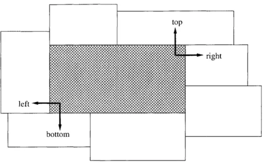
Figure 2-2: Corner-stitched CRectangle object.
Specifically, FluidLayout represents a VLSI layout as a set of corner-stitched rect-angles, as discussed in [14]. Figure 2-2 illustrates the corner-stitching of a rectangle.
This corner-stitching allows for time searching of a CLayer object and
linear-time area enumeration.
To do this, each CRectangle object has a GotoPoint method. Given a CRectangle
R and a destination point in the CLayer containing R, GotoPoint follows the top
and bottom pointers to reach the desired ordinate and then follows the left and right pointers to reach the desired abscissa. Since following left and right may
cause deviation from the desired ordinate, this procedure must be iterated until the rectangle at the destination point is found. However, since the stitched objects are
convex, the algorithm is guaranteed to terminate [14].
Similarly, each CLayer object has a Paint method derived from [14]. Paint al-lows the caller to paint a rectangular region of the layer. All CRectangle objects that
intersect this rectangular region are clipped against it, and the material types of the
resulting pieces are adjusted to perform the painting. The enumeration of rectangles
within the clipping region is done in linear time by the following procedure: by follow-ing down and right pointers from the upper-leftmost rectangle, the rectangles along
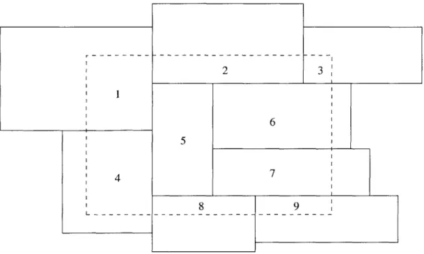
2 3 I 1 6 5 I 4 7 8 9
Figure 2-3: Area enumeration of CRectangle objects within a bounding rectangle.
the left edge of the clipping rectangle may be identified. For each of these, horizontal swaths of the clipping region may be enumerated by following right pointers. A
sample area enumeration is shown in Figure 2-3.
The relevant VLSI algorithms can be expressed in terms of searches and area enu-merations and are thus carried out efficiently in FluidLayout. For example, placement of a wire is done by selecting the rectangular areas where metal is desired and calling
the Paint method on those areas. Viewing the circuit in the GUI is done by
enu-merating the rectangles within the view rectangle. For each enumeration, Windows
drawing methods are called to render the rectangle.
All that remains for implementation is the interconnection of distinct 2-D layers into a 3-D circuit.
2.2.2 Circuit Partitioniing
There are many possible approaches to the problem of partitioning 3-D circuits among
new fabrication technologies require extensive modification to the technology support in the software. For example, suppose that a 2-D design package has support for a two-poly, three-metal CMOS process. If the technology for four metal layers is developed, the design package must be modified to accommodate the new metal layer, both in the internal representation and in the GUI. While the internal representation may be readily modifiable or may already support arbitrary technologies, modifying or extending the GUI is nontrivial, and in fact, 2-D design packages generally do not have support in the GUI for arbitrarily many material layers.
On the other hand, FluidLayout can support arbitrarily many material layers without modification of the 2-D slice object structure and without extensions to the GUI. This is accomplished by assigning a finite number of material layers to each 2-D slice and alloying the number of slices to vary arbitrarily. Each 2-D slice is assigned gate, source/drain, and semiconductor material as well as two metal layers and all inter-layer vias. The slice is also provided with vias from the top metal layer to the gate layer of the next slice, thus forming the inter-slice interconnect. This material set is necessary and sufficient to create arbitrary circuits within an individual 2-D slice.
Arbitrary technology mappings can then be implemented by ignoring portions of slices as necessary. For example, a 3-D process with six interconnect layers per slice may be implemented by pairing adjacent CLayer objects and ignoring the semiconduc-tor material on the second CLayer of each pair. Also, a 2-D process with arbitrarily many metal layers can be implemented by ignoring all semiconductor material except on the lowest slice.
The canonical technology in FluidLayout is centered around a bottom-gate thin-film transistor structure [21]. Each layer of transistors is thus represented as a set of TFTs along with two metal layers. This results in the technology shown in Figure 2-4. With the implementation framework thus described, FluidLayout is able to per-form various system-level procedures, such as circuit verification through netlist ex-traction and circuit fabrication.
gate (next layer) q metal2 6 metall semiconductor ~Tsource/drain gate
Figure 2-4: Canonical technology used in FluidLayout.
2.3
Circuit Verification
One of the main advantages of having CAD software with integrated 3-D capabilities
is that the software can perform tasks such as circuit netlist extraction. FluidLayout is able to extract connectivity information from 3-D integrated-circuit layouts.
In order to perform this netlist extraction, FluidLayout separates a given layout
into planes, where each plane contains a given material (gate, source/drain, metall, or metal2) and the vias that connect that material to the next higher material along the third dimension. Then, FluidLayout enumerates all the rectangles in each plane,
starting with the lowest. Each rectangle is checked to see if it belongs to a previously-defined electrical node. FluidLayout then checks adjacencies to determine if two nodes have been assigned to a single wire, and if so, merges the nodes. Finally, if
the rectangle is not assigned to a node, and is not adjacent to a node, a new node is created. Further, if the rectangle is part of a via, the corresponding rectangle on the
next plane up is marked and added to the node. This allows the extraction procedure to maintain electrical connectivity along the third dimension.
In FluidLayout, a CWire object is used to identify a node. Each CWire object contains a list of pointers to the CRectangle objects associated with the node. Each
CRectangle object has a generic pointer that is used in netlist extraction to point to the CWire object to which the rectangle belongs. Thus, when the area enumeration
is complete, all electrical nodes in the circuit have been identified, and each rectangle is able to identify the node to which it belongs.
layout. The semiconductor rectangles are enumerated, and surrounding gate and source/drain rectangles are identified. Each valid combination of gate, source, and drain is used to construct a CTransistor object that identifies the electrical nodes for the gate, source, and drain and the width and length of the transistor channel. The list of CTransistor objects is then written to a text file using the standard SPICE format for MOSFETs.
2.4
Circuit Fabrication
One motivation for writing FluidLayout is to have the ability to support any fabri-cation technologies that emerge in the laboratory. For example, it is desirable to be able to target designs for an inkjet nanoparticle MEMS process [7] or a VLSI/MEMS liquid embossing process [16], without having to modify the layout.
Support in FluidLayout for these facilities is provided by integrating methods that handle the circuit extraction into the document class. For each fabrication process, different file formats must be exported to support the fabrication. For example, the target inkjet process is a 3-D gantry system that is computer-controlled and requires G-code. The process prints materials in the same way that an inkjet printer prints rectangles, so in FluidLayout, there are methods to extract the separate material layers and raster the individual rectangles. Similarly, the liquid embossing process uses an elastomeric stamp to separate a film of solution into desired and undesired regions. A rectangular wire is thus created using a stamp whose raised surface is the outline of the rectangle. When pressed onto a uniform film, the stamp then drives away liquid corresponding to the wire outline. These stamps are created from wafers, which are created using lithographic masks. These masks are specified using the GDSII binary file format, so FluidLayout has methods for converting a set of rectangles to their outlines and writing these outline rectangles to GDSII binary output.
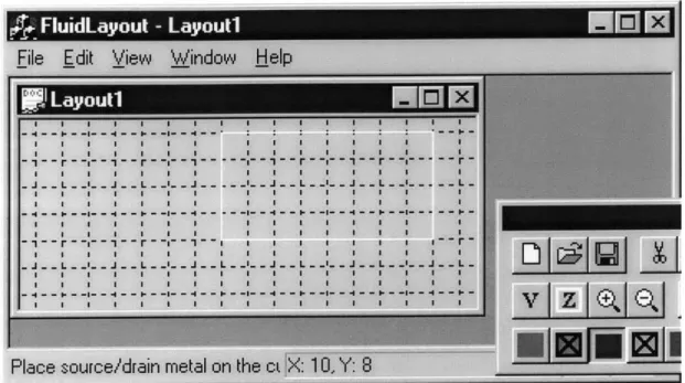
Place source/drain metal
Figure 2-5: Box-outlining is used to place materials in FluidLayout.
2.5
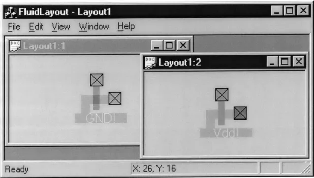
Design Walk-Through
To demonstrate the use and capabilities of the FluidLayout software, FluidLayout is used here to lay out an inverter. A more complete walk-through is available in Appendix A.
Figure 2-5 shows the use of box outlines, drawn by left-clicking at the lower left and right clicking at the upper right, to place materials in the layout.
By using the materials toolbar, layout of an n-channel MOSFET is completed on the first layer, as shown in Figure 2-6.
Interconnect to layer 2 is done through a via from the top metal on layer 1 (i.e., metal2) to the gate metal on layer2. As shown in Figure 2-7, the via is placed on layer 1. FluidLayout marks a corresponding via on the second layer, as can be seen
in the view window for the second layer.
A p-channel MOSFET is laid out on the second layer, and the complete inverter is shown in Figure 2-8.
Figure 2-6: Complete NMOS pulldown path.
Ready
|X:14,
Y: 20Figure 2-7: Placement of a metal2-+gate via results in a gate-+metal2 hint on the second layer.
Figure 2-8: The complete inverter.
feature is used. The feature size is set to 5 microns per unit grid length (lambda). The following is the circuit netlist produced:
***** C:\WINNT\Profiles\shamikd\Desktop\inverter. sp
***** Created by FluidLayout ***** Created on 5/1/2000 M1 2 3 GND! 0 NTFT W=15u L=10u M2 2 3 Vdd! Vdd! PTFT W=15u L=10u
This SPICE deck may then be used for verification of the layout.
A more comprehensive guide to using FluidLayout can be found in Appendix A.
As shown here, FluidLayout is a useful software CAD system for laying out and fabricating 3-D circuits. These capabilities will now be demonstrated with several test circuits.
Chapter 3
Some Basic Transistor Circuits
The immediate application of FluidLayout is in targetting simple, commonly-known circuits for an emerging three-dimensional fabrication technology. This allows both for testing the functionality of FluidLayout and for exploring the viability of the technology.
3.1
Minimum Criteria for the Technology
A new transistor technology is viable for computation only if suitable multi-transistor devices can be fabricated. In particular, it is possible for transistors to provide non-linear input-output behavior, yet still be unsuitable for multi-transistor circuitry. There are several criteria that need to be met. These criteria are evaluated within the context of the metal-insulator-semiconductor field-effect technology discussed in
[17, 16].
Consider, for example, the NMOS inverter in Figure 3-1. The desired function of this inverter is to take the signal represented by in and produce the logical negation of that signal at out. Represented using voltages, therefore, if V1 is below VM, then V0t should be above VM, and vice versa, where VM is some midpoint voltage
between Vdd and ground. To verify that this circuit produces the desired behavior, the characteristics of the individual transistors must be examined.
Vdd
(W/L)
1out
in
(W/L) 2
Figure 3-1: NMOS inverter.
The governing I - V relationships for the n-channel FET are given as follows:
ID (L) ( ( Vn~ins GS V DSn DS
for VGS - VTn VDS (the linear regime) and
ID,SAT = I AnCins
(+)
(VGS - Tn )2(1 + AnVDS)for VGS - VTn < VDS (the saturation regime), where pn is the field-effect mobility, Cin, is the gate insulator capacitance, W/L is the transistor channel width-to-length ratio,
VGS is the gate-source voltage, VTn is the threshold voltage, VDS is the drain-source
voltage, and An is the channel-length modulation parameter [9].
It is clear, then, that this type of circuit produces the desired operation: for a low input voltage, transistor 2 is turned off and transistor 1 pulls the output voltage high, and for a high input voltage, transistor 2 is turned on, thus pulling the output voltage low, provided transistor 2 is stronger than transistor 1. Transistor 2 is thus called a pulldown, while transistor 1 is called a pullup.
As important as functionality, however, is the ability of the inverter to restore logic levels. That is, while a 0 is represented ideally by 0 volts and a 1 is represented ideally by Vdd, in actuality, this is not necessarily the case. However, a functioning
9 M1
Vout
r 0
0~
vf
r
0v
Figure 3-2: NMOS inverter small-signal model about VM.
logic gate should to some extent recognize and accommodate these deviations from ideality. Consider, for example, a series of cascaded inverters, each of which outputs 0 volts for an input of Vdd and vice versa. Suppose the input to the first is slightly less than VXd, say Vdd - AVi. The output of this inverter will then be greater than 0 volts
by some amount, say AVst. If the inverter restores logic levels, then AV,0 t < AV". If this is not the case, then as the signal passes through each inverter, the deviation from the ideal will increase until the signal stabilizes at VM.
Level restoration follows if the gain of the inverter at VM is greater than one in magnitude. Consider an inverter whose output is Vdd minus the input. Then the gain at VM is identically -1, and deviations in the input are reflected exactly in the output.
The gain of the inverter in Figure 3-1 at the midpoint voltage VM can be de-termined by examining the small-signal model of this inverter, shown in Figure 3-2. From the model, it follows that the gain of the inverter is
yout _ m2ro
where gm is the small-signal transconductance, defined as gm = 2pCims (EL) ID,SAT,
and r, is the small-signal output resistance, defined as r, = (AID,SATY 1
[9].
Thus, having a large transconductange and a large output resistance is critical to the per-formance of the inverter: consider the cases where gmir, is small or is large. If the product gmiro is small compared to 1, then the gain is essentially -gm2ro/2, which is also small. If, on the other hand, gmiro is sufficiently large, then the gain is approx-imately -gm2/gm1 = g. The transistor sizing is thus dictated by the need for high gain.The technology described in [17, 16] features transconductances on the order of
10-5 S and output resistances on the order of 106Q for a device with W = 292.5 pm and L = 2 pm at a VM of about 10 volts. This indicates that a gain of greater than unity is achievable with device sizes that currently can be fabricated.
3.2
Design of Basic Circuits
In order to test both the fabrication technology and the capabilities of FluidLayout, some simple circuits are laid out using FluidLayout, and fabrication-ready output is produced. The layout used here consists of an inverter, a NOR gate, a basic static memory cell, and two ring oscillators.
The inverter implementation used in this layout is that in Figure 3-1. The device sizes used are channel length of 10 pm, a channel width of 200 pm for the pullup FET, and a channel width of 1200 pm for the pulldown FET. Using the above device parameters, this should provide a gain of approximately -1.5.
The NOR gate uses two pulldown transistors wired in parallel. Each is identical in size to the inverter pulldown.
The memory cell, discussed in detail in Chapter 4, uses a pair of coupled inverters together with two access transistors.
Finally, the two ring oscillators are different layouts of the same circuit. This circuit comprises three inverters wired in a series loop. Provided that the inverters have sufficient gain, a latent signal on an input to one of the inverters is amplified to
Figure 3-3: Layout of test devices.
Vdd or to ground as it passes through the inverters. Further, when the signal returns
to its starting point, it does so as its inverse, so that the signal oscillates when viewed at any fixed point. However, if the inverters do not have sufficient gain, the signal will decay to the midpoint voltage, VM. Thus, a ring oscillator is an ideal circuit to test intrinsic device parameters.
Further, it is possible to examine different layout strategies with this multi-gate circuit. In particular, the second ring oscillator, though electrically identical to the first, is partitioned along the third dimension into three layers, with one inverter on
each layer. Power and ground signals are distributed through vias to the upper layers, and the return signal from the output of the last inverter to the input of the first inverter travels through a via stack located near the outputs.
- a
B
if
Figure 3-4: 3-D layout of a ring oscillator. The three inverters shown are stacked to form the 3-D layout.
The first layer of the layout of the entire structure is shown in Figure 3. Figure 3-4 shows the 3-D layout of the ring oscillator, including the 2nd and 3rd layers of the layout.
In order to verify the functionality of the devices in this structure, the SPICE netlist is extracted using FluidLayout.1
***** C:\WINNT\Profiles\shamikd\Desktop\Maskl.sp
***** Created by FluidLayout
***** Created on 5/1/2000
*** inverter
M1 invout inv_in GND! 0 NTFT W=1200u L=10u M34 invout Vdd! Vdd! 0 NTFT W=200u L=10u
*** NOR gate
M2 norout norA GND! 0 NTFT W=1200u L=10u M3 norout norB GND! 0 NTFT W=1200u L=10u
M35 norout Vdd! Vdd! 0 NTFT W=200u L=10u
*** SRAM cell (4,7 are internal bit storage nodes) M4 7 sramWL sramBL 0 NTFT W=200u L=10u
M13 sramBLBAR sramWL 4 0 NTFT W=200u L=10u
M5 7 4 GND! 0 NTFT W=1150u L=10u M6 GND! 7 4 0 NTFT W=1150u L=10u M36 7 Vdd! Vdd! 0 NTFT W=150u L=10u
M37 Vdd! Vdd! 4 0 NTFT W=150u L=10u
*** 2-D ring oscillator (three inverters)
M14 6 ring GND! 0 NTFT W=1200u L=10u
M38 6 Vdd! Vdd! 0 NTFT W=200u L=10u
M15 5 6 GND! 0 NTFT W=1200u L=10u M39 5 Vdd! Vdd! 0 NTFT W=200u L=10u
M16 ring 5 GND! 0 NTFT W=1200u L=10u
M40 ring Vdd! Vdd! 0 NTFT W=200u L=10u
'This SPICE deck has been edited for clarity. For example, with typical circuit layouts, the area enumeration algorithm results in all the n-channel devices grouped together and all the p-channel devices grouped together. The SPICE deck shown here has the transistors grouped by function. Also, since one of the features of the technology is the ability to route gate across source or drain, the netlist extraction will sometimes output a transistor as a parallel combination of two or more smaller transistors. This will allow for more accurate capacitance modelling once the relevant parameters have been obtained from the technology. However, in the SPICE deck shown here, parallel transistors have been merged.
*** 3-D ring oscillator
M29 3 ring_3D GND! 0 NTFT W=1200u L=10u
M41 3 Vdd! Vdd! 0 NTFT W=200u L=10u
M42 2 3 GND! 0 NTFT W=1200u L=10u
M47 2 Vdd! Vdd! 0 NTFT W=200u L=10u M48 ring_3D 2 GND! 0 NTFT W=1200u L=10u
M53 ring-3D Vdd! Vdd! 0 NTFT W=200u L=10u
Functional simulation can then be performed using this netlist to verify the
per-formance of the circuits.
The circuit can now be extracted to output that can be used for fabrication. The process in [17, 16] uses elastomeric liquid embossing to form circuit patterns. Each material layer (gate, source/drain, etc.) is patterned using a unique part of the stamp.
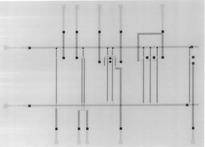
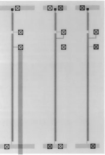
This stamp is created using a wafer as a mold. Thus, FluidLayout is used to extract the circuit to a GDSII binary stream that can be used to fabricate a wafer mask. This mask pattern is shown in Figure 3-5.
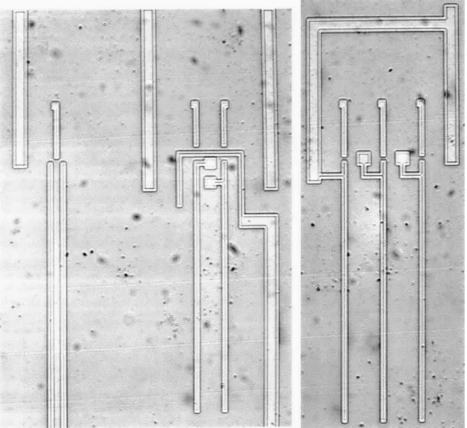
From this mask, an elastomeric stamp is created. This stamp is used to pattern solution-processed materials, which are then cured. The resulting structures form the gate, source/drain, semiconductor, and interconnect for the circuits. For example,
Figure 3-6 shows the gate metal for the NOR gate, SRAM cell, and 2-D ring oscillator. Figure 3-7 shows the source/drain metal for these circuits. Thus, FluidLayout is useful
both for laying out circuit structures and for fabrication of these circuits.
For the remainder of this thesis, some designs will be examined that utilize more of the potential of FluidLayout. In particular, the focus is no longer on rapid prototyping of three-dimensional integrated circuits, but instead on exploring the architectural
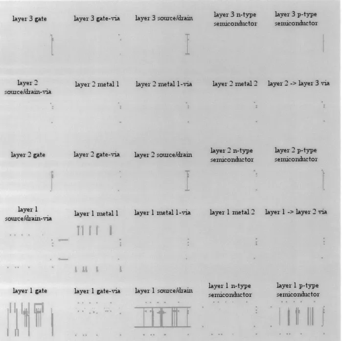
layer 3 pte-via
I
layer 2 somreMrain-via
layer 2 metal layer 2nuttl- ayvi2 nmtti2 lUavr 2 -> lApr 3 via
e-pe layer 2 gate-via i layer 1 sourceldrain-via layer 1 gate
IM-I
layer 1 metal lTI1
i1'
I iL Ilayer I zstul 1 -ia layer 1 retal 2
ser % ukto r
-layer I - layer.12 via
I
layer 1 gate-via
I
layer 1 source/dain layer 1 n-type smnicnductor
layer 1 p-type semicondutor
Figure 3-5: Stamp pattern with spatially-separated material patterns.
I111-
t
layer 2 gate
liarige 3 -y
laye r 13 a= eem l
-. C I C a
B
Fl
V
ii
H 0 a47
4I
4
-S0 4
1.r
AI
-0 4 *K
~
~'It
~____ a 'I -- k-a-Iji : "7 9e* 1: ~ .0: -K
1'
-'I SiK'
I--,
_p
-Yr
Figure 3-7: Patterned source/drain for a NOR gate, SRAM cell, and ring oscillator.
2
41