Defect Engineering in Cuprous Oxide (Cu
2O)
Solar Cells
by
Sin Cheng Siah
M. S., (Mechanical Engineering)
Massachusetts Institute of Technology, 2013
B. Eng., (Engineering Science)
National University of Singapore, 2010
ARCIVES
MASSACH-ETT INSTITUTE OFTENLLG
JUL 3
02015
LIBRARIES
Submitted to the Department of Mechanical Engineering
in partial fulfillment of the requirements for the degree of
Doctor of Philosophy in Mechanical Engineering
at the
MASSACHUSETTS INSTITUTE OF TECHNOLOGY
June 2015
Massachusetts Institute of Technology 2015. All rights reserved.
A uthor...
C ertified by...
Signature
redacted
..
...I
...
N
... ...
.
Department of Mechanical Engineering
May 19, 2015
Signature redacted
Tonio Buonassisi
Associate Professor of Mechanical Engineering
Thesis Supervisor
Signature redacted
A ccep ted b y ...
...
David E. Hardt
Professor of Mechanical Engineering
Chairman, Department Committee on Graduate Theses
Defect Engineering in Cuprous Oxide (Cu20) Solar Cells
by
Sin Cheng Siah
Submitted to the Department of Mechanical Engineering on May 19, 2015 in Partial Fulfillment of the
Requirements for the Degree of
Doctor of Philosophy in Mechanical Engineering
ABSTRACT
This thesis is focused on the development of a cuprous oxide (Cu2O) thin-film (TF) solar cell that is fabricated by manufacturing-friendly methods such as electro-deposition, sputtering and atomic layer deposition. Due to its bandgap of close to 2 eV, it has the potential of being applied as top cell in a tandem configuration. Firstly, I perform bottom-up cost and price analysis to investigate the economic feasibility of TF and c-Si based tandem photovoltaic modules. Next, I investigate the formation of good ohmic back contacts on Cu20 absorber layer and demonstrate that low contact resistivity can be achieved with a variety of metals on heavily doped Cu20 films
by forming a tunnel junction. Then, I apply synchrotron-based X-ray absorption spectroscopy (XAS) to characterize two front contact buffer materials: amorphous Zn-O (a-ZTO) and
Sn-doped Ga2O3. I elucidate a fundamental loss mechanism in the amorphous Zn-Sn-O (a-ZTO) electron-blocking layer that has origin in local structural disorder and establish the structure-process-property relationship of a-ZTO so that the front buffer layer can be optimized for photovoltaics. Then, I investigate the doping mechanism of Sn dopant atoms in TFs and single crystalline Ga2O3:Sn by revealing the doping mechanism so that Ga203:Sn can be optimized for photovoltaics. Lastly. I apply bulk defect engineering to manipulate the intrinsic point defect structure of Cu20 towards improved device performance. The key results will inform the processing conditions for improving mobility and minority carrier lifetime in Cu20.
Keywords - Earth-abundant, thin-film solar cells, tandem, defect engineering, cost modeling,
synchrotron.
Thesis Supervisor: Tonio Buonassisi
ACKNOWLEDGEMENTS
I would like to express my utmost gratitude to my advisor, Professor Tonio Buonassisi, for
his guidance, and motivation over the past five years. I have not only picked up a tremendous amount about research from Tonio, but also learnt a lot about being a good family man.
I am also thankful to Yun Seog Lee, Rafael Jaramillo, Riley E. Brandt, Jonathan P. Mailoa
and Michael Lloyd. They have each contributed in ways that have been invaluable to this research project. Douglas M. Powell is acknowledged for his mentorship on cost modeling. Sarah E. Sofia and Marius I. Peters are acknowledged for their contributions in the cost modeling work. Sergio Castellanos is acknowledged for being an exercise and thesis-writing buddy. My gratitude also goes out to all fellow colleagues of the PVLab for the constant intellectual stimulations during group meetings and all the fun and joyful memories during the group's recreational activities. Being so far away from home is a big challenge and would have been much more difficult without the great support from the PVLab.
A big part of my PhD involves synchrotron-based X-ray spectroscopy techniques and I
would like to thank Grant B. Bunker for introducing me to the world of synchrotrons through the
XAS summer school in 2012. I am deeply grateful to Michael F. Toney, Carlo U. Segre and
Steve M. Heald for giving me the opportunities to conduct experiments at their beam-lines. I am also grateful to Chengjun Sun, Tomohiro Shibata, Laura. T. Schelhas, Kipil Lim and Joshua Wright for their help during synchrotron runs.
I am also extremely grateful to the National Research Foundation of Singapore for
supporting my graduate studies at a leading technology institute through a Clean Energy Scholarship. Finally, I would like to thank my family, my girlfriend Serene Tan, and friends for their unwavering love and support back home in Singapore.
CONTENTS
Abstract ... 3
Acknow ledgem ents...5
Contents...7
Figures ... 1
Citations to Published W ork...15
Chapter]: Introduction ... 17
1.1 Photovoltaics as a Sustainable Energy Source ... 17
1.1.1 Terawatts Scalability: Earth-Abundant Thin-Film Solar Cells ... 18
1.1.2 State-of-the-art of Cu20 Solar Cells... 21
1.2 Thesis Overview ... 22
Chapter 2: Bottom-Up Techno-Economic Analysis of Thin-Film and c-Si Based Tandem Solar Cells...25
2.1 A bstract...25
2.2 Introduction...25
2.3 Cost and M inim um Sustainable Price M odels... 27
2.3.1 Bottom-Up Manufacturing Cost Analysis for PV Modules ... 27
2.3.2 M inim um Sustainable Price for PV M odules ... 30
2.3.3 Calculation of Total System Installation M SP... 30
2.4 Results and D iscussion... 31
2.4.1 Econom ic Feasibility of TF Single Junction M odules ... 31
2.4.2 Economic Feasibility of c-Si Based Tandem Modules ... 34
2.5 Conclusions...38
Chapter 3: Principles of Defect Engineering ... 39
3.1 Introduction...39
3.2 Engineering Back Contact... 40
3.2.2 Measuring Contact Resistivity and Schottky Barrier Height...42
3.2.3 Measuring Schottky Barrier Height... 43
3.2.4 Lowering Contact Resistivity Using a Tunneling Layer ... 44
3.3 Engineering Front Hetero-Junction... 45
3.3.1 Importance of Recombination at Hetero-Junctions... 45
3.3.2 Effects of Band Alignment and Interface States at Hetero-Junction... 46
3.3.3 Measuring Band Alignments ... 47
3.4 Engineering Bulk Defects... 48
3.4.1 Importance of Bulk Defects in Thin-Film Solar Cells ... 48
3.4.2 Extrinsic Doping in n-type buffer layers ... 49
3.4.3 X-ray Absorption Spectroscopy as a Local Probe of Atomic Environment ... 49
3.4.4 Bulk Recombination and Point Defects Structure in Cu20 ... 51
3.4.5 Lifetime and Photoluminescence Spectroscopy... 52
Chapter 4: Low Contact Resistivity of Metals on Nitrogen-Doped Cuprous Oxide (Cu2O) Thin-F ilm s ... 5 5 4 .1 A b stract...5 5 4 .2 Intro ductio n ... 56
4.3 Experimental Methods... 57
4.4 Results and Discussions... 58
4.4.1 Undoped Cu20/Metal Contacts: Schottky Barrier Height and Chemical R eactiv ity ... 5 8 4.4.2 Nitrogen Doping Reduces Metal/Cu20 Contact Resistivity and Changes Conduction Mechanism ... 61
4.4.3 Nitrogen Doping Enables Low-Resistivity Contact for Earth-Abundant Metals 64 4.5 Application of Cu20:N Layer in Solar Cell... 65
4 .6 C onclu sio ns...66
Chapter 5: Impact of Structural Disorder on Electron Mobility in Amorphous Zinc-Tin-Oxide B uffer L ayers ... 69
5 .1 A b stract...6 9 5 .2 Intro d uctio n ... 70
5.3 Experim ental Details... 73
5.4 Results and Discussions ... 74
5.5 Conclusions... 8 1 Chapter 6: Dopant Activation in Sn-Doped Ga2O3... 83
6.1 Abstract...83
6.2 Introduction...84
6.3 Experimental Details... 85
6.4 Results and Discussions ... 87
6.5 Conclusions...)9 1 6.6 Supplemental M aterial ... 92
Chapter 7: Bulk Defect Engineering in CU20 ... 93
7.1 Abstract ... 93
7.2 Introduction... 94
7.3 Experimental M ethods ... 95
7.4 Results and Discussions ... 97
7.5 Conclusions...100
Chapter 8: Conclusions ... 103
FIGURES
Figure 1.1: Distribution of global primary energy demand by 2050 as predicted by the German
Advisory Council on Global Change, from Reference.2 The scenario is predicted based on
extrapolation of current expansion rates of various renewable energies. ... 18
Figure 1.2: Scatter plot of elemental market price against production volume. The estimated production volume and elemental market price required to reach I TWp is indicated by the solid lines. A dapted after Lloyd et al. ... . . . .. . . 20
Figure 2.1: Typical manufacturing process flow of a TF solar cell...27
Figure 2.2: Merging c-Si and TF cost models to yield a tandem module cost model. ... 28
Figure 2.3: Sensitivity of estimated BoS price to module efficiency from SAM. ... . . . . 31
Figure 2.4: Cost breakdown and MSP for a TF module with q = 14.5% in terms of (a) process step and (b) component. The capex for deposition of absorber is $10/M2 and absorber-related material cost is $5/M2. The MSP is estimated assuming WACC = 14%. ... 32
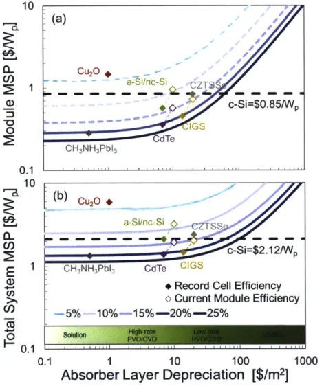
Figure 2.5: Sensitivity of (a) module MSP and (b) total system MSP of various TF technologies to absorber deposition capex and module efficiency. The black dash line represents the module MSP or system MSP for c-Si. The symbols represent several technologies and are estimated based on their efficiency, estimated materials-related cost and estimated deposition capex. The open symbols represent current record cell efficiency and the closed symbols represent the typical m odule efficiency in the market... 33
Figure 2.6: Schematic drawings of a 2-terminal (a) mechanically stacked tandem module and (b) monolithically integrated tandem module ... 35
Figure 2.7: Sensitivity of (a) module MSP and (b) total system MSP of i = 30% tandems to absorber deposition capex and module efficiency. The black dash line represents the module MSP or system MSP for c-Si. The colored dashed lines are for single junction TF modules for co m p ariso n ... 36
Figure 2.8: Sensitivity of total system MSP of q = 30% tandems to absorber deposition capex as a function of module efficiency. The black dash line represents the system MSP for q = 20.5% c-Si. The colored dashed lines are for single junction TF modules for comparison. ... 37
Figure 3.1: Liebig's Law of the Minimum adapted to solar cells, from Ref. 28. ... 40
Figure 3.2: (a) SCAPS simulation for a metal/Cu20/Ga203/ZnO:Al solar cell with different work function for the metal back contact and (b) device structure used for SCAPS simulations...41 Figure 3.3: (a) Circular contact pattern for CTLM and (b) cross-section of CTLM. ... 43 Figure 3.4: Schematic illustrating the effect of doping on holes transport across the M-S interface, (a) thermionic emission, (b) thermionic field emission, and (c) field emission...45 Figure 3.5: (a) J-V characteristics of solar cells with and without a highly doped layer and (b) energy band diagram at Voc condition, illustrating the narrow depletion width at the back contact region, resulting in tunneling transport. The conduction band (Ec), electron quasi-Fermi level
(EFn), hole quasi-Fermi level (EFp) and valence band (Ev) are indicated on the energy band d iag ram ... 4 5
Figure 3.6: SCAPS-simulated results for (a) different interface states densities, and (b) different conduction band offsets...47
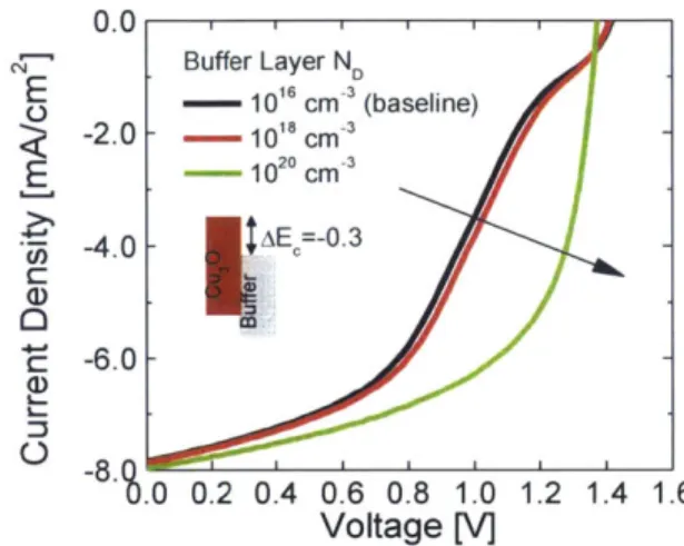
Figure 3.7: SCAPS-simulated J-V characteristics for Cu20-based solar cells with different buffer d o p ing d ensities. ... 4 9
Figure 3.8: Equilibrium Fermi level and defect concentrations calculated for Cu-rich/O-poor conditions and Cu-poor/O-rich conditions. The hole concentration and Fermi level are given both in equilibrium at growth temperature Tg and at room temperature 298 K. This figure is from R aeb ig er et a l. ... 52
Figure 4.1: Cu 2p core level photoemission for (a) Au, (b) Ag and (c) Pd samples. A peak shift towards lower binding energies is observed for the Pd samples, indicating the lowering of the SBH. A high binding energy shoulder due to CuO can be observed...58 Figure 4.2: Illustration of method to determine the SBH from the XPS data from the valence-band spectra (right) and Cu 2p core level spectra (left) of (a) bare Cu20 film and (b) Cu20 film
with two nm Au overlayer. The Fermi level is calibrated using the Fermi edge of Au. All spectra have been corrected for charging by using the adventitious C Is peak. ... 59
Figure 4.3: Photoemission from metallic peaks of samples with 2 nm thick (a) Au, (b) Ag and (c) Pd overlayers. A high binding energy shoulder due to PdO can be observed. ... 60
Figure 4.4: Contact resistivity is plotted against Cu20 nitrogen doping concentration for three contact m etals: A u, A g, and Pd... 62
Figure 4.5: Contact resistivity as a function of measurement temperature for Pd on CU20 with three doping concentrations. Similar behavior (not shown) is also observed for Au and Ag samples. The solid black line represents a fit to a thermionic emission model; the dashed red and blue lines are guides to the eye. ... 63
Figure 4.6: Plot of the ratio kT/Eoo as a function of hole density (p) with m*=3.36m0 and e = 7.OEo. The dotted line indicates that the ratio kT/Eoo = I and both thermionic emission and field
effect processes are comparable. kT/Eoo for both undoped ([N] = 0.0 at.%, p = 3.7x 1015 cm-3) and lightly ([N]= 0.6 at.%, p = 1.8x1018 cm-3) doped samples are indicated on the plot...64 Figure 4.7: Contact resistivity as a function of measurement temperature for Cu, Ni and Pd on
highly doped ([N] = 1.2 at. %) samples. The dashed lines are guides to the eye. ... 65
Figure 4.8: (a) A cross-sectional SEM image of a Cu20-based TF solar cell with a Cu20:N hole-transporting layer. Dashed lines (white) indicate interfaces between layers, and (b) J- V characteristics of a Cu20:N and a control Cu20 device under I sun illuminated (AM 1.5 G, 100
mW cm-2
) condition. Figures are from Lee et al.6 1... . . . .. . . 66
Figure 5.1: (a) J-V characteristics of Au/Cu20/ZTO/ZnO:AI/Al solar cells fabricated with a-ZTO of different compositions and (b) Relative alignments of conduction band (CB) and valence band (VB) for a-ZTO and ZnO overlayers to Cu20 TFs as measured by XPS. Plots reproduced
fro m L ee et al.13. . . . . ... 7 1
Figure 5.2: Capacitance-frequency measurements for Au/Cu20/a-ZTO/ZnO:Al/Al solar cells fabricated with a-ZTO of different compositions. ... 72
Figure 5.3: Fourier-transformed EXAFS spectra at Zn and Sn K-edges. Figures (a) and (b) compare the peak intensity of the INN shell at the Zn and Sn K-edges respectively. The arrows illustrate the decreasing peak intensity with increasing [Sn]. Figures (c) and (d) show the
measured (symbols) and fitted spectra (lines) at the Zn and Sn K-edges respectively (offsetted for c larity ). ... 7 6
Figure 5.4: XANES spectra at (a) Zn and (b) Sn K-edges. The 2 isosbestic points are circled and labelled A and B in (a)...78
Figure 5.5: Field-effect/Hall-effect mobilities, device efficiency and pseudo-Debye-Waller factors are plotted against [Sn]/([Sn]+[Zn]) ... 79
Figure 6.1: Net carrier density of P-Ga2O3:Sn single crystals as a function of varying [Sn], compared against the deduced upper limit for a-Ga203:Sn films...86 Figure 6.2: Sn edge XANES spectra for (a) SC fl-Ga203:Sn, (b) PLD Ga2O3:Sn and (c) ALD a-Ga203:Sn samples. The dashed, dashed-dotted and dotted lines represent Sn(0) metal (blue), Sn(lI)O (green) and Sn(IV)02 (purple) references respectively...88
Figure 6.3: Fourier-transformed EXAFS spectra plotted as the magnitude, IX(R)I, for (a) Ga and
(b) Sn K-edges. The spectra for SnO and Sn02 are included as reference...89
Figure 7.1: (a) A typical sample under illumination by microscope light. Sample is glowing red due to its bandgap. (b) A microscope image of a similar as-grown foil under 50x magnification. Scale bar represents 1000 tm ... 96
Figure 7.2: Time-temperature profiles for the growth and annealing process of Cu20 samples. (N ot draw n to scale)...96
Figure 7.3: Measured sheet resistance, Hall-mobility and effect hole concentration for samples grown with varying Tanneal. The lines are guides for the eye. ... 98
Figure 7.4: [t-PCD decay transients for all samples. A double exponential behavior can be observed for sam ples at low Tanneai...98 Figure 7.5: (a) Spectrally-resolved PL for sample with no annealing, or Tanneal = 24"C and (b) PL
imaging of all samples. The defect-band that is being imaged is shown schematically in (a)...99 Figure 7.6: (a) TpCD as a function of the inverse of spatially-integrated PL intensity (PLI) and (b)
CITATIONS TO PUBLISHED WORK
Parts of this dissertation cover research reported in the following articles:
[1] S. C. Siah, Y. S. Lee, Y. Segal, and T. Buonassisi, "Low contact resistivity of metals on
nitrogen-doped cuprous oxide (Cu20) thin-films," J. Appl. Phys., vol. 12, no. 8, p. 084508, 2012.
[2] S. C. Siah, S. W. Lee, Y. S. Lee, J. Heo, T. Shibata, C. U. Segre, R. G. Gordon, and T. Buonassisi, "X-ray absorption spectroscopy elucidates the impact of structural disorder on electron mobility in amorphous zinc-tin-oxide thin films," Appl. Phys. Lett., vol. 104, no. 24, p. 242113, Jun. 2014.
[3] S. C. Siah, R. E. Brandt, L. T. Schelhas, K. Lim, J. D. Perkins, R. Jaramillo, M. D.
Heinemann, D. Chua, J. Wright, C. U. Segre, R. G. Gordon, M. Toney, T. Buonassisi, "Dopant activation in Sn-doped Ga2O3 investigated by synchrotron-based X-ray absorption spectroscopy," (in preparation for submission).
[4] Y. S. Lee, D. Chua, R. E. Brandt, S. C. Siah, J. V Li, J. P. Mailoa, S. W. Lee, R. G. Gordon, and T. Buonassisi, "Atomic Layer Deposited Gallium Oxide Buffer Layer Enables 1.2 V Open-Circuit Voltage in Cuprous Oxide Solar Cells," Adv. Mater., vol. 26, no. 27, pp.
4704-4710, May 2014.
[5] Y. S. Lee, J. Heo, M. T. Winkler, S. C. Siah, S. B. Kim, R. G. Gordon, and T. Buonassisi,
"Nitrogen-doped cuprous oxide as a p-type hole-transporting layer in thin-film solar cells,"
J. Mater. Chem. A, vol. 1, no. 48, p. 15416, 2013.
[6] Y. S. Lee, J. Heo, S. C. Siah, J. P. Mailoa, R. E. Brandt, S. B. Kim, R. G. Gordon, and T.
Buonassisi, "Ultrathin amorphous zinc-tin-oxide buffer layer for enhancing heterojunction interface quality in metal-oxide solar cells," Energy Environ. Sci., vol. 6, no. 7, p. 2112,
CHAPTER
1
INTRODUCTION
1.1
Photovoltaics as a Sustainable Energy Source
During the industrial revolution in the 18th century, there was a heavy demand for
mechanical machines to drive manufacturing processes. Demand for energy in the form of fossil
fuels to power these machines increased dramatically and since then, mankind never looked
back. Global energy consumption is now estimated to be more than 1.7x 10¹⁴ kW-h and is
expected to grow by
53%
over the next 20 years.' While standard of living has improved as a
result of this revolution, continued unsustainable use of resources to meet our insatiable thirst for
energy has resulted in undesirable impacts on Earth's environment. The unsustainable use of
resources has led to a plethora of problems that include air and water pollution, depletion of
natural resources and global climate change. According to a report published by the International
Panel on Climate Change (IPCC), high-accuracy measurements have provided evidence for the
direct correlation between warming of the Earth's atmosphere to human activities.
1High profile
reports by climate champions such as former U.S. Vice president Al Gore and the IPCC have
strongly advocated for the mitigation of these negative impacts on the Earth's climate by moving
towards a future that is built upon energy sustainability.
One viable option to reduce mankind's reliance on conventional energy sources is to adopt
renewable energies as alternatives. As illustrated in Figure 1.1, the German Advisory Council on
important by 2050.2 It can be seen that conventional fossil fuels are not expected to be totally replaced but their overall contribution is expected to decrease significantly over the next 40 years. On the other hand, renewable energies are expected to increase their relative contribution to the energy distribution. In particular, solar is an attractive alternative due to the vast amount of energy Earth receives from the Sun every day. To put things into perspective, the Earth receives about 5.5x 10¹⁷ kW.h of energy from the Sun annually. This is about 3200 times the world total energy consumption in 2013. Solar energy can be harvested in various forms including heat (solar thermal) and electricity (photovoltaics). In this thesis, the main focus will be on photovoltaics (PV). The goal of solar PV is to convert a fraction of this enormous resource from the sun into electricity.
700-Primary energy saving
600 Savings through:
E Wind and solar
500 CHP and heat pumps generated gas
Direct energy generation M Solar power
400 (wind, solar, hydro) M Wind
* Solar heat M Geothermal power 3 Hydropower M Biomass heat 200 l Biomass power E Nuclear energy 100 E1 Natural gas M Crude oil M Coal 0 1970 1980 1990 2000 2010 2020 2030 2040 2050 Year
Figure 1.1: Distribution of global primary energy demand by 2050 as predicted by the German Advisory Council on Global Change, from Reference.2 The scenario is predicted based on extrapolation of current expansion rates of various renewable energies.
1.1.1
Terawatts Scalability: Earth-Abundant Thin-Film Solar Cells
In 2014, worldwide PV production is about 38.7 GWp,3 and solar cells based on crystalline silicon (c-Si) make up over 90% of the industry. The remainder of the PV market consists of
solar cells based on thin-film (TF) technologies such as amorphous silicon (a-Si), cadmium
telluride (CdTe) and copper indium gallium diselenide (CIGS). Work by Powell et al.4 has
shown that in c-Si PV manufacturing, upfront capital cost or capital expenditure (capex) associated with producing polysilicon as well as material cost associated with feedstock silicon can be substantial. For example, the capex associated with building a 400 MWp c-Si solar cells manufacturing factory can be more than $272 milliona. The cost of the silicon feedstock is about
$0.10/Wp
or >15% of the total cost for c-Si PV.4 The high capex, high feedstock cost andextensive silicon requirement associated with silicon PV might eventually be an impediment to terawatts (TW) scalability.
The low cost per unit area of TF technologies makes it a leading candidate to achieve lower than $0.50/Wp module cost. It also has improved potential to reach TW scalability due to a I00x reduction in material requirement for the light-absorbing layer. However, conventional TFs solar cells using CdTe and CIGS absorbers could be limited to sub-terawatt deployment due to material scarcity (Te and In) and toxicity (Cd) issues.5 To guide material selection for the TF PV
absorber layer, Lloyd et al.6 estimated the material production and price required to achieve terawatts scalability. Figure 1.2 plots the selling price of materials against their production in
2010. To achieve I TW production annually the annual production of the chosen material should
be more than 1500 tonnes per year and the elemental selling price of the material should be less than $250/kg (assuming a 2 ptm absorber). By assuming a binary semiconductor consisting of an
Earth-abundant cation metal (- $250/kg) and anion chalcogen or oxygen (- $1/kg), the upper
bound of the material cost for a 2 pm thick absorber layer is estimated to be $2.5/M2 (yield
=50%).
Elemental Market: Modes of Production
106
Os 0
105 * Primary U Primary/Secondary Secondary
104 Rb TM S103 xe Re Ge toT big Kr $250/kg 4 102 Nb H 10 C o 100 so 100B
B
101O NaM
10-2 Ca 10-2 10.1 100 101 102 103 104 10S 106 107 108 109 1010 10"2010 Production (Tonnes)
Figure 1.2: Scatter plot of elemental market price against production volume. The estimated production volume and elemental market price required to reach I TWp is indicated by the solid lines. Adapted after Lloyd et al.6
Based on a list of low-cost sustainable elements, Lee et al.7 performed first-principles calculations to search for possible compound semiconductors using a combinatorial method. Subsequently, extensive literature review and further first-principles calculations are used to narrow down the list and eventually, identified cuprous oxide as a promising candidate among others like zinc phosphide (Zn3P2), copper nitride (Cu3N), silicon diphosphide (SiP2).8 While
there is certainly a long list of semiconductors that satisfy the criteria mentioned above, the technical work performed in thesis will primarily focus on engineering and enhancing Cu20-based solar cells and maximizing its potential as a future PV material. In principle, the structured
approach to improve performance presented herein can be generalized to other promising compounds.
1.1.2 State-of-the-art of Cu20 Solar Cells
Prior to 2006, the efficiency of Cu20-based solar cells remained below 2%. The main reason
for low performance, was the inability to find a good conjugate n-type partner for Cu20. In 1983,
Olsen et al.9 demonstrated a conversion efficiency of 1.8% using Cu20/Cu Schottky junction
solar cells. These Schottky cells are based on polycrystalline Cu20 wafers grown using thermal oxidation of copper foil and demonstrated carrier collection as high as 10 pm. The relatively high collection length resulted in short-circuit currents (Jsc) as high as 8 mA/cm2, and it was
estimated that Jsc could reach at least 12 mA/cm2 by incorporating a more transparent front
contact. On the other hand, the low open-circuit voltage (Voc) of below 400 mV was attributed to the formation of a copper-rich region at the hetero-interface which limited barrier height and
consequently, the Voc. It was hypothesized by Olsen et al.9 that the development of
homojunction or better control of interfacial properties would be critical for the success of Cu20.
In 2006, Mittiga et al.'0 improved the Voc of Cu20-based solar cells to 600 mV by incorporating
a zinc oxide (ZnO) buffer layer to form a hetero-junction solar cell. Subsequently, the use of zinc
magnesium oxide (a-Znu.x)MgxO),1, 2 amorphous zinc tin oxide (a-ZTO),' "4 and amorphous
gallium oxide (a-Ga2O3)1,16 as buffer layers have contributed to Voc improvements over the
years. In particular, a record Voc of 1.2 V was achieved using a-Ga2O3 grown by atomic layer deposition on electrodeposited Cu20."
This thesis is mainly focused on elucidating the physics that is driving these recent improvements, and to provide outlook for future improvements. We note that tandem devices are
particularly sensitive to top-cell performance, because the top cell supplies roughly two thirds of the tandem output power.
1.2
Thesis Overview
To provide the thesis with a broader perspective, Chapter 2 focuses on addressing scalability issues pertaining to TF PV manufacturing. A cost model for a hypothetical TF PV manufacturing factory is developed and the impact of absorber-related capex and material costs on the minimum sustainable price of TF modules is investigated. Subsequently, the model is extended c-Si or TF based tandem solar cells.
Chapter 3 provides a brief overview of defect engineering concepts that are relevant to the scope of the thesis. Results from SCAPS simulations are shown to highlight the importance of back contact, front contact and absorber bulk engineering and to provide a framework for improving the performance of Cu20 solar cells. In addition, brief descriptions of different characterization techniques are presented.
Chapter 4 investigates the formation of low-resistivity ohmic back contacts to Cu20. Contact resistivity of various metals, both precious and Earth-abundant, is quantified. A scheme of introducing a highly doped Cu20 as tunneling layer is introduced to significantly reduce contact-resistivity for metals that form a Schottky barrier at the back contact.
Chapter 5 elucidates the physics behind the relationship between device efficiency and bulk electronic and structural properties of a-ZTO buffer layers. Band alignment measurements are performed to relate device efficiency to energy band structure at the hetero-junction. In addition, synchrotron-based X-ray absorption spectroscopy is used to relate structural properties of a-ZTO films to mobility and solar cell performance.
Chapter 6 discusses the physics underlying a high Voc obtained with a-Ga203 buffer layer and emphasize the importance of doping the buffer layer to further improve efficiency. In addition, synchrotron-based X-ray absorption spectroscopy is used to understand the doping mechanism of Sn-doped Ga203 so as to help guide the development of highly conductive Ga203 thin films.
Chapter 7 examines the relationship between growth process, electronic properties and defect structure of Cu20. Complementary characterization techniques such as spectrally-resolved
photoluminescence, defect-band photoluminescence imaging, microwave reflection
photoconductance decay lifetime measurement and Hall measurements are used to derive useful information about the bulk electronic properties of Cu20.
CHAPTER
2
BOTTOM-UP TECHNO-ECONOMIC
ANALYSIS OF THIN-FILM AND C-SI
BASED TANDEM SOLAR CELLS
2.1
Abstract
The cost advantages of thin-film (TF) and c-Si based tandem solar cells are not well studied and are less obvious as compared to conventional single-junction solar cells. In this chapter, module minimum sustainable selling price (MSP) and total photovoltaic (PV) system MSP models are developed for both types of solar cells with an emphasis on understanding the impact of TF or top cell absorber deposition on economical feasibility. Without restricting the analyses to any particular material system but generalizing it more broadly to various manufacturing approaches, the costs associated with TF absorber growth techniques are surveyed and investigated. The sensitivity of MSP and total system installation MSP for TF and tandem modules towards module efficiency and capital expenditure (capex) is investigated. It is found that balance of system (BoS) costs drive the economic feasibility of high-efficiency approaches and make high-efficiency c-Si based tandems more financially attractive.
2.2
Introduction
The cost-competitiveness of electricity generation is determined by the amount of money it costs to generate one watt of electricity. For PV, it has been recognized that the following
simplified expression relates cost of PV to manufacturing and installation costs and module performance:1 7'1 8
Cost of PV [$W] = Manufacturing Cost [$/M2] + Installation Cost [$/m2 and $/W,] (2.1)
Module Efficiency [W/m2]
Ultimately, the cost of PV plays a huge role in determining the economically feasibility of PV technologies and there exist many pathways to lower the cost of PV. In this chapter, two promising ways are addressed: 1) TF solar cells with low manufacturing and upfront capital costs and 2) c-Si based high efficiency tandem solar cells. These two approaches are not necessarily mutually exclusive because cost-effective TF solar cells can be used to complement existing c-Si solar modules by operating in tandem.
The chapter will begin by introducing the bottom-up cost assessment approach which is an accounting exercise used to sum up every cost components across the PV value chain. Once the bottom-up cost accounting is completed, the MSP can be estimated by additional financial considerations.4,19-21 The emerging view of the topic is that capex is one of the main drivers of MSP due to cost of capital associated with an upfront capital investment. For a fixed module selling price, a higher capex will reduce the profit margin and leads to a slower growth rate for the manufacturing company. In light of this, the subsequent part of this chapter will be dedicated to understanding the influence of capex on MSP for various technologies. A strong focus will be made on the growth of TF absorbers because other module-related costs like electrodes deposition, laser patterning, encapsulation, framing and wiring are expected to be standard across different TF technologies. Without restricting the analysis to any particular material system but generalizing it more broadly to manufacturing approaches, the capex and materials cost associated with TF absorbers fabricated using various techniques are surveyed and compared. These techniques are broadly classified into four different categories: solution-based processing,
high-rate physical and chemical deposition, low-rate physical and chemical deposition and
epitaxy deposition.
The analysis is then extended to c-Si based tandem PV modules by combining the cost
model for TF solar cells with existing c-Si cost model. In both scenarios, the main issue to be
discussed pertains to the impact of absorber-related capex on module MSP and total system MSP
of the respective PV technologies. The results from these analyses can help guide selection of
materials and growth techniques, as the cost savings [$/W] attainable for tandem modules can be
expressed as a trade-off between a decrease in area-related costs due to efficiency improvements
and an increase in costs associated with top-cell manufacturing and integration. Lastly, module
efficiencies that will enable each of these manufacturing methods be economically viable and
exceed the target of US$0.50/W are estimated.
2.3 Cost and Minimum Sustainable Price Models
2.3.1 Bottom-Up Manufacturing Cost Analysis for PV Modules
Glass Laser Bc
Cleaning Patterningn
FrntBuffer Layer Laser
Deposition Patterning
Laser Absorber Modularization
Patterning Deposition
Figure 2.
1:
Typical manufacturing process flow of a TF solar cell.Figure 2.1 shows a typical manufacturing process flow of a TF module. In this case, a superstrate structure is assumed in which the front electrode is deposited first. Nevertheless, this
model is also applicable to a solar cell grown in substrate configuration since it will consist similar number of process steps, only in a different sequence. This will also form a baseline in which the capital and materials costs associated with absorber deposition step can be
investigated.
In general, the direct manufacturing costs associated with each process step can be divided into five components: depreciation, direct materials, utilities, labor, and maintenance overhead. In accrual accounting, the depreciation expense [$/Wp or $/m2] of each step is defined as capex
allocated over the period of time when related revenue is generated (matching principle). In this work, a throughput-normalized capex [$/(Wp.yr) or $/(m2.yr)] is used to calculate depreciation expense so that different deposition techniques are compared on equal footing. Table 2.1 summarizes the various assumptions that are used for each component. In addition to the various process steps illustrated Figure 2.1, the costs associated with building a factory and cleanrooms are also included under 'facilities'. Repetitive steps such as laser patterning and electrode deposition are accounted for by a multiplication factor. It is important to note that the purpose of this model is not to predict manufacturing costs of TF PV modules with pin-point accuracy, but to highlight dominant factors and general trends.
Bottom Cell Cost Model Top Cell Cost Model
c-Si thin-film
Tandem Cell Cost Model c-Si +thin-film
Figure 2.2: Merging c-Si and TF cost models to yield a tandem module cost model.
To model the cost structure of c-Si based tandem modules, the TF module cost model is combined with existing model for a / = 16% c-Si module4 as shown schematically in Figure 2.2.
Table 2.1: Summary of the assumptions used for each process step to model the cost structure of a hypothetical TF PV manufacturing line. The numbers are not adjusted for yield and only represents a single repetition.
Step Component Depreciation Materials Utilities Labor Maintenance Depreciation Materials Utilities Labor Maintenance Depreciation Materials o .5 Utilities 0 & Labor Maintenance Depreciation 8 Materials Utilities Labor Maintenance Depreciation Materials Utilities Labor Maintenance e Depreciation Materials Utilities Labor Maintenance Cost [$/m2 ] 1.9 x 10⁻¹ 0.000 0.375 0.426 5.3 x 10⁻⁶ 0.007 5.660 0.375 0.426 0.002 2.000 3.000 0.375 0.426 0.560 x 2.500 0.375 0.426 0.28x 0.500 0.000 0.375 0.426 0.140 0.022 17.82 0.375 0.426 0.006 Assumption
Similar to c-Si cell and module manufacturing.4 Materials in operation phase is negligible.
Total electricity consumption similar to c-Si cell plant.4 Estimated using methodology in Powell et al.4
28% of depreciation.
Estimated using data from glass cleaner supplier. Includes a piece of glass.
Total electricity consumption similar to c-Si cell plant.4 Estimated using methodology in Powell et al.4
28 % of depreciation.
Estimated using data from PVD equipment supplier. Estimated using data from PVD equipment supplier. Total electricity consumption similar to c-Si cell plant.4 Estimated using methodology in Powell et al.4
28 % of depreciation. Vary x from 0.1 to 1000.
Fixed at $2.5/M2.
Total electricity consumption similar to c-Si cell plant.4 Estimated using methodology in Powell et al.4
28 % of depreciation.
Estimated using data from laser supplier. No materials needed.
Total electricity consumption similar to c-Si cell plant.4
Estimated using methodology in Powell et al.4
28 % of depreciation.
Estimated using data from laminator supplier.
Includes encapsulant, glass, Al frame and junction box.4 Total electricity consumption similar to c-Si cell plant.4 Estimated using methodology in Powell et al.4
Table 2.11: Cost breakdown in c-Si module manufacturing for
20.5% advanced concept c-Si module.4
Component Cost [$/m2] Depreciation 14.90 Materials 57.19 Utilities 7.08 Labor 16.7 Maintenance 5.52 Total 101.39
(a) q = 16% baseline c-Si module and (b) q =
Component Cost [$/m2 ] Depreciation 14.98 Materials 38.12 Utilities 5.97 Labor 7.72 Maintenance 5.48 Total 72.27 (a) (b)
2.3.2 Minimum Sustainable Price for PV Modules
Manufacturing cost does not necessarily translate directly to selling price. However, applying certain financial considerations to a cost structure can allow the lower bound on a sustainable price be estimated. This price is so-called the MSP and is calculated using a discounted cash flow model for a hypothetical 400 MW factory. It is the price at which the internal rate of return equals the WACC and more details about calculating MSP is described by Powell et al.4 The role of the MSP is to take into account the cost of capital of initial outlay to build a working manufacturing facility. Consequently, the difference between cost and MSP can be mostly attributed to the weighted average cost of capital (WACC) and capex.
2.3.3 Calculation of Total System Installation MSP
To fully capture the effect of module efficiency, the total PV system installation cost is calculated by taking into account BoS costs. The total BoS cost is sensitive to PV conversion efficiency as many factors such as land requirement and mounting hardwares scale with total installation area. In this work, BoS-related costs for 2015 and the SunShot target for 2020 are obtained from the Solar Advisor Model (SAM) developed by the National Renewable Energy Laboratory.2 3 Here, the term 'BoS MSP' is used because the profit-margin for PV installation is
1
nn
-BoS in 2015 -SunShot Goal in 2020 5 5.0 0 Ca 0.0 0.0% 10.0% 20.0% 30.0% 40.0% Module EfficiencyFigure 2.3: Sensitivity of estimated BoS price to module efficiency from SAM.23
Figure 2.3 shows the sensitivity of BoS price in 2015 and the projected SunShot target for
2020. At low efficiencies, the BoS price varies greatly with module efficiency due to costs that
scale with installation area. Hence, the cost-effectiveness of a PV installation depends on the
trade-off between BoS and module price.
2.4 Results and Discussion
2.4.1 Economic Feasibility of TF Single Junction Modules
Figure 2.4 (a) and (b) show the cost breakdown for a TF module with r7
=
14.5%, absorber
deposition capex = $10/m
2and absorber materials-related cost = $2.5/m
2. Here, the capex of
$10/M2 assumes a high-rate physical vapor deposition process (based on internal market
research) and a material cost of $2.5/m2, which is determined as a reasonable upper bound for an
Earth-abundant semiconductor that has potential for TW scalability following Figure 1.2. The
model estimates a cost and MSP of $0.40 and $0.63 respectively, highlighting the prospect for
Earth-abundant TF modules to achieve < $0.50 total manufacturing cost. It can be observed that
the total cost comprises of a large fraction of materials related cost
(-
56%) whereas capex
makes up about 26%. This cost structure is typical for both organic and inorganic TF modules
-which can be made using high-throughput processes that significantly reduces capex or
processing costs.
0.70 0.70 O.63 0.63 0.60 0.60 Framing and wiring 0.50 0.50 w Encapsulation w Maintenance OH sP 0...~a.
Laser Patterning 0.40 WLabor 0.40* Utilities m Top Cell
3 0 Materials Deposition
3CAPEX 0.30 w Contact
Deposition
U)*Estimated NSP (
0.20 0m0.20 Substrate Glass &
Cleaning a Facilities and OH 0.10 0.10 + Estimated MSP 0.00 0.00
(a)
(b)
Figure 2.4: Cost breakdown and MSP for a TF module with 'i = 14.5% in terms of (a) process step and (b) component. The capex for deposition of absorber is $1 0/m2 and absorber-related material cost is $5/M2. The MSP
is estimated assuming WACC = 14%.
Figure 2.5 (a) shows the sensitivity of MSP to absorber capex for a single-junction TF
module and compares the module MSP for various TF PV technologies. Similarly, the
iso-efficiency lines are determined by assuming an absorber materials-related cost = $2.5/m
2and
other parameters as summarized in Table 2.11. For the various TF technologies that are
represented in Figure 2.5, the materials-related cost and capex associated with the absorber layer
are estimated using the elemental market price chart in Figure 1.2 and internal market research
respectively. It can be observed that when capex is low, the MSP becomes limited by materials
cost and MSP reduction can be achieved by improving efficiency or reducing materials cost. The
record Cu20 device efficiency grown using a low capex method (electro-deposition) is
3.9%.15
The model suggests that to attain cost-competitiveness in module MSP with existing c-Si,
efficiency should be at least 7%. Based on the estimation carried out in this work, it can be
modules. Increasing efficiency while keeping the same cost structure can allow both CdTe and
CIGS to approach a module MSP of below $0.60/Wp. The emerging methylammonium lead(II)
iodide perovskite (CH
3NH
3PbI
3) is particularly attractive from a cost perspective due to a low
capex associated with solution-based processing methods. However, long-term stability issues
due to moisture, heat
4and UV light" have to be resolved before CH
3
NH
3PbI
3can be
commercially viable.
10
(a)
-L CU20 U 1 a-si/nc-Si C ZT2c-Si=$0.85/W,
S1----GS
0 CH3NH3Pbl3 dTe 0.1 10-IL
(b)
Cu 20+ a-Si/nc-Si CZT SS-
c-Si=$2.12/W,
E
1
CH3NH3Pbl3 CdTe CIGS4) +
Record Cell Efficiency
o
Current Module Efficiency
S
5%- 10%-15%-20%-25%
0.1
0.1 1 10 100 1000
Absorber Layer Depreciation [$/m
2]
Figure 2.5: Sensitivity of (a) module MSP and (b) total system MSP of various TF technologies to absorber deposition capex and module efficiency. The black dash line represents the module MSP or system MSP for c-Si. The symbols represent several technologies and are estimated based on their efficiency, estimated materials-related cost and estimated deposition capex. The open symbols represent current record cell efficiency and the closed symbols represent the typical module efficiency in the market.
As mentioned earlier, the module MSP by itself is an inadequate gauge because module efficiency has a significant influence on costs incurred further downstream of the PV value chain. For a more comprehensive analysis, the total system MSP is calculated and compared in Figure 2.5 (b). The total system MSP is calculated by summing the module MSP, BoS costs, and
installer's profit margin as described in section 2.3.3. Because the total system MSP comprises a large portion of BoS-related costs which are mostly area-related, it is more sensitive to module efficiency. By taking this effect into account, the financial barrier for low efficiency technologies becomes significantly higher as observed in Figure 2.5 (b). Correspondingly, r/ should approximately be greater than 15% for TF PV to make economic sense on a utility scale if absorber deposition capex is greater than $1 0/m2. It is worth cautioning that apart from economic feasibility, there are other barriers which can play an important role in commercial viability manufacturing scalability. These include (but no limited to) module reliability (which influences
the weighted average cost of capital), process complexity, yield and performance
reproducibility.22
2.4.2 Economic Feasibility of c-Si Based Tandem Modules
While c-Si based tandems is a high efficiency approach which can potentially leverage on existing c-Si manufacturing factories, the economic feasibility is not well studied and will be address partly in this section. The main question that will be addressed pertains to the economic viability of c-Si based tandem. Although the analyses performed in this section are for c-Si based tandems, most learnings can be generalized to other tandem structures.
The most straightforward scenario for a tandem module to make economic sense is if the combined MSP is cheaper than the MSPs of both the top and bottom module in a situation which they are to operate individually:
MSPanemcell
<Min[M
P,.ceS M SPottomcei] (2.2)This scenario will provide the financial incentives for both top and bottom cell manufacturers to
pursue the tandem approach. In this section, the economic feasibility of tandems will be
investigated from two different perspectives: module MSP and total system MSP. As shown in
Figure 2.6, two different tandem structures are studied in this work: (a) mechanically stacked
tandem in which a TF module is mechanically stacked on top of a c-Si module, and (b)
monolithically integrated tandem in which additionally absorber, buffer and contact layers are
grown monolithically on c-Si solar cells to yield a tandem solar cell. In the first scenario, the
entire cost structure of a top cell module is added onto c-Si's module cost whereas in the latter
approach, only the costs associated with absorber and electrodes depositions are included. The
monolithic approach is more streamlined because the total modularization cost is significantly
reduced.
++
(a)
(b)
Figure 2.6: Schematic drawings of a 2-terminal (a) mechanically stacked tandem module and (b) monolithically integrated tandem module.
Figure 2.7 (a) shows the sensitivity of the MSP for a q
=
30% tandem (mechanically stacked
and monolithically integrated) to absorber capex as compared to c-Si and single junction TF. The
mechanically stacked tandem has a higher MSP due to additional costs related to modularization.
The cost advantages of both types of tandem module are negligible especially at low top cell
absorber deposition capex because the MSP for TF top modules with q
>
10% will be lower than
both q = 16% bottom c-Si and q
=
30% tandem modules. As a result, the window is very narrow
for tandems to be successful just by comparing module MSP. Physically, it is also very
challenging to attain a q/ = 30% tandem module with a top cell q < 10%.
10
a-a
-c-Si=$0.85IW~
0.1' 10 -(b) 5% 10% 15% -- 20% 0.1 0.1 1 10 100 1000Top Cell Absorber Depreciation [$/m 2]
Figure 2.7: Sensitivity of (a) module MSP and (b) total system MSP of ' = 30% tandems to absorber deposition
capex and module efficiency. The black dash line represents the module MSP or system MSP for c-Si. The colored dashed lines are for single junction TF modules for comparison.
Similarly, the cost advantage of a high efficiency approach can only be fully understood by
looking beyond module MSP and considering the total system MSP instead. Figure 2.7 (b) shows
that the total system MSPs of both tandem approaches are below that of c-Si and a r/ = 20% TF. It can be observed that the window for tandems to be successfully is now significantly wider.
or lower (monolithically integrated) than -both a q = 20% top TF module and a q = 16% c-Si
bottom module. The technological barrier to achieve a q = 30% tandem module with a q = 20%
top TF module and a q
=
16% c-Si bottom module is also much lower, especially if the bandgap
of the top module is near optimal. These results are promising as efforts have already been made
to demonstrate significant boost in overall efficiencies by combining these perovskite cells with
c-Si or CIGS cells.
26 2710
E
c-si=$1.07/WP
Monolithic q=30% Tandem
-
5%
10%
15% - - 20%
F-0.10.1
1
10
100
1000
Top Cell Absorber Depreciation
[$/m
2]
Figure 2.8: Sensitivity of total system MSP of I = 30% tandems to absorber deposition capex as a function of module efficiency. The black dash line represents the system MSP for q7 = 20.5% c-Si. The colored dashed lines are for single junction TF modules for comparison.
Projecting forward to the next 5 years, the efficiency of the bottom c-Si module is assumed
to reach q = 20.5% and achieve a MSP of $0.5 1/Wp.4 BoS price will also continue to decline as
described in Figure 2.3. Under these assumptions, the 'sweet spot' window is predicted to shrink
as shown in Figure 2.8, mainly due to reductions in the MSP of c-Si and area-related BoS costs.
Nonetheless, tandems can still remain feasible economically and have the potential to achieve close to $1/Wp total installed MSP. In particular, a monolithic tandem will have greater success
2.5
Conclusions
In summary, module MSP and total system MSP are modeled for TF and c-Si based tandems. It is shown that area-related BoS costs drive the economic viability of high-efficiency PV technologies. Consequently, it becomes important to take into account total system MSP when considering the feasibility of different technologies. For TF PV, it is found that q > 15% is required to make economic sense on a utility scale. For both monolithically and mechanically integrated c-Si based tandem structures with / = 30%, it is found that the total system MSPs are below those of the bottom q = 16% c-Si module and top / = 20% TF module. This presents an exciting opportunity for the commercialization of tandem PV technologies based on c-Si. Lastly, projections made toward 2020 predict that there exist opportunities for tandems to be economically feasible despite reductions in c-Si module MSP and various area-related BoS costs.
CHAPTER
3
PRINCIPLES OF DEFECT ENGINEERING
3.1
Introduction
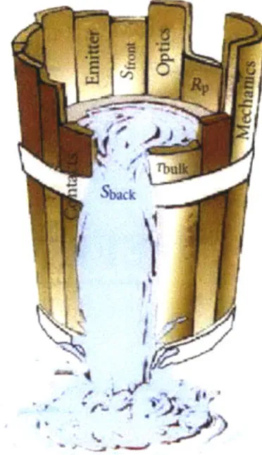
Defects present in bulk, interfaces and surfaces can have detrimental effects on solar cell performance. Consequently it is important to understand their origins and engineer solutions to mitigate their negative impacts. A famous German chemist named Justus von Liebig came up with the Law of the Minimum which essentially states that the water level in a barrel is limited
by the length of the shortest stave, emphasizing the need to identify and mitigate the most
limiting factors so improve performance. Glunz adapted it for silicon solar cells development as shown in Figure 3.1 to illustrate efficiency bottlenecks.2 8 In general, the same law is applicable to the development of TF solar cells in which identifying limiting loss mechanisms is crucial for efficiency improvements. In this respect, some critical issues of interest typically pertain to recombination processes in different regions of a solar cell, metal back contact formation and
optical light trapping. To this end, back contact, interface and bulk defect engineering are discussed in relation to Cu20 solar cell performance in this chapter as background and to motivate work in later chapters.
Figure 3.1: Liebig's Law of the Minimum adapted to solar cells, from Ref. 28
3.2
Engineering Back Contact
3.2.1 Forming Ohmic Back Contact
For a solar absorber, the back metal contact is responsible for extracting the photo-generated majority carriers (i.e., holes for p-type and electron for n-type). Consequently, forming low-resistivity ohmic contacts on a solar absorber is a critical step to reduce power loss. However, the formation of an ohmic metal-semiconductor (M-S) contact can be complicated due to a variety of reasons such the formation of a Schottky barrier, surface Fermi level pinning and chemical reactions at the M-S interface which introduces secondary phases. These issues have been discussed comprehensively by Schroder29 and a brief summary is included in this section.
The Schottky model is the simplest model which describes the barrier height, 0B at M-S interface is given as:29
B =OM -X for n-type (3.1)
#B
=Eg + X -# mfor
p-type (3.2)where X is the electron affinity of the semiconductor, $m is the work function of the metal and
E. is the bandgap of the semiconductor. To the first order, a suitable metal can be chosen in
consideration of the semiconductor's X so that
#B
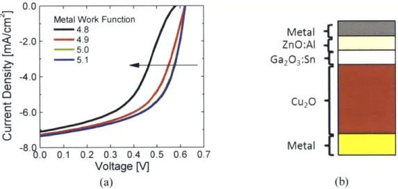
is as small as possible. Figure 3.2 shows the
SCAPS-simulated impact of metal work function on metal/Cu20/Ga2O3/ZnO:Al solar cell. The
parameters used for SCAPS simulations are similar to those report by Brandt.
30As Cu20 has ;r
= 3.2 and E. = 2.0, a metal Om = 5.1 yields the highest efficiency due to good alignment with
the valence band of Cu20. A roll-over characteristic can be observed for Om= 4.8 eV due to the
formation of a barrier with $B= 0.3 eV.
0.0
E Metal Work Function
4.8 Metal -2.0 - 4.9 ZnO:Al E - 5.0 - 5.1 Ga2
O
3:Sn -4.0-CU2-
Cu
2O c: -6.0--8.Q 'Metal 0.0 0.1 0.2 0.3 0.4 0.5 0.6 0.7 Voltage [V](a)
(b)
Figure 3.2: (a) SCAPS simulation for a metal/Cu2
0/Ga
2O3/ZnO:Al solar cell with different work function for the metal back contact and (b) device structure used for SCAPS simulations.In reality, the simple model does not predict trends observed for some semiconductors
including Ge and Si due to the formation of oxide, although it works well for silicides.
29Work
level and make
#B
independent of 0, . Following Bardeen's model, Cowley and Sze has shown that the barrier height (for n-type semiconductor) can be expressed by:#B
=v(M - X) + (I -)(Eg --#0
) (3.3)where E. is the bandgap of the semiconductor, 0 is the position of the charge neutrality level measured from the top of the valence band and y is a "pinning factor" which is related to the thickness and total permittivity of the oxide layer at the interface and the density of surface states.
While Schottky's model offers a good first-order guide for selecting an appropriate metal back contact, it is often more complicated due the presence of surface states and oxides.
Consequently, direct measurements of contact resistivity and
#B
across the M-S interfaceprovide a more realistic approach to select and evaluate ohmic contacts suitable for device applications.
3.2.2 Measuring Contact Resistivity and Schottky Barrier Height
The most common way to measure specific contact resistivity (pc ) of a M-S interface is through the transmission line model. A linear transmission line model required mesa etching to prevent unwanted conduction pathways while a circular transmission line model (CTLM) eliminates the mesa etching step, hence simplifying test-structure fabrication.32