Design of Curved Electrodes to Enable Large Stroke
-
Low Voltage Micro Actuators
by
Eric B. Newton
B.S. Engineering Physics and Mathematics
University of Wisconsin - Madison 2009S.M. Mechanical Engineering
Massachusetts Institute of Technology 2012
Submitted to the Department of Mechanical Engineering
in Partial Fulfillment of the Requirements for the Degree of
Doctor of Philosophy in Mechanical Engineering
at the
MASSACHUSETTS INSTITUTE OF TECHNOLOGY
February 2016
02016 Massachusetts Institute of Technology
All rights reserved
Signature of Author:
Certified by:
Accepted by: MASSACHUSErTS INSTITUTE OF TECHNOLOGYMAR
0
2
Z016
LIBRARIES
MCVES
Signature redacted
Eric B. Newton
Department of Mechanical Engineering
A,-
n
-September 3, 2015
Signature redacted
Martin A. Schmidt
Professor of Electrical Engineering and Computer Science, Provost
Thesis Supervisor
Signature redacted_____
.%j
Rohan Abeyaratne
Professor of Mechanical Engineering
Chairman, Committee for Graduate Students
MITLibraries
77 Massachusetts Avenue
Cambridge, MA 02139 http://Iibraries.mit.edu/ask
DISCLAIMER NOTICE
Due to the condition of the original material, there are unavoidable
flaws in this reproduction. We have made every effort possible to
provide you with the best copy available.
Thank you.
The images contained in this document are of the
,best quality available.
Design of Curved Electrodes to Enable Large Stroke
-
Low Voltage Micro Actuators
by
Eric Newton
Submitted to the Department of Mechanical Engineering
on September 3, 2015, in Partial Fulfillment of the requirements for the degree of Doctor of Philosophy in Mechanical Engineering
Abstract
Electrostatic actuators are common in many MicroElectroMechanical Systems (MEMS) devices. These actuators tend to be fabricated as two parallel planar structures, which works well for applications where the motion and electrode spacing are small. To achieve larger displacements, very large voltages are needed. Curved electrodes provide a way to create actuators that achieve large displacements and large forces at much lower voltages than comparable parallel plate designs.
This thesis describes two methods for creating curved silicon membranes that can be easily integrated into practical devices. The first method uses air pressure to plastically deform a silicon membrane at high temperature. During wafer bonding, gas is trapped behind a thin silicon membrane. High temperature annealing causes the gas to pressurize, plastically deforning the silicon membrane. A model predicting the extent of plastic deformation was matched with actual deformation measurements. The second method utilizes the strain resulting from curing epoxy. A diaphragm is formed by etching through the handle of an SOI wafer, leaving a circular silicon membrane. After filling the etched hole with epoxy and covering it, the epoxy shrinks and pulls the membrane into a curved shape.
These curved membranes have been integrated into electrostatic actuators. Pull-in was demonstrated on devices with a wide range circular membranes. The actuation is reliable and requires relatively low voltages. A first order model based on the principle of virtual work was developed that accurately predicts the onset of pull-in. Predictions are compared for several electrode profiles and in every case the critical voltages were lower than for parallel plates.
Finally, the design of a MEMS vacuum pump that incorporates curved electrostatic actuators is analyzed. Factors that affect the base pressure, such as dead volume and pumping volume, are discussed in detail. With low leak rates, base pressures as low as 0.24 Torr could be achieved in these devices in a two stage pump. Guidelines for the design and operation of future MEMS diaphragm pumps are proposed.
Thesis Supervisor: Martin A. Schmidt
Acknowledgements
I feel quite lucky to have had such a rewarding graduate experience. Throughout the last six years, I have been surrounded by people who were both very knowledgeable and happy to offer their advice on all sorts of questions. I would like to thank them for their support - I would not have finished without their help.
First and foremost, I would like to thank my adviser, Professor Martin Schmidt, who has provided constant guidance and support since I joined the group. He readily shares his
knowledge and passion of both MEMS research and the industry surrounding it. Marty has the gift for asking critical questions that have pushed me towards becoming the researcher that I am today. I would also like to thank all of my labmates Eric, Parker and Mitchell for their friendship and support. Parker and Mitchell answered countless questions about mechanical designs and have cheerfully helped me by machining simple parts. My officemate Eric Lam listened to me vent about cleanroom problems countless times, and provided a solid sounding board when I ran into research problems.
I owe a debt of gratitude to Dr. Hanqing Li. Much of what I know about
microfabrication, especially deep reactive ion etching and wafer bonding, I learned from him. His cleanroom expertise has helped me through many fabrication conundrums. On top of all of that, he had enough faith in me to recommend me to my future employer. I also want to my committee members, Evelyn Wang and Sang-Gook Kim. They provided insightful feedback during our meetings. I would also like to thank my previous adviser Professor Carol Livermore
for taking me into her research group when I arrived at MIT. She helped me adjust to graduate life and allowed me to get my first experience with MEMS. I want to thank the exceptional MTL staff for training and assistance in the clean room. I am particularly thankful to Dennis Ward and Donal Jamieson, who gave crucial insight into my fabrication process and helped troubleshoot problems when processing did not go as planned.
I would like to acknowledge my family for the continuous moral support they have provided me with throughout this process. I do not know how I would have made it through the last several years if you had not been there for me. I especially want to thank my wife Rocio for helping me with my throughout my studies. She has seen me at my worst, through quals and while trying to wrap up the thesis, and her support has never wavered. I can safely say that I would not be where I am today without her love and support.
Table of Contents
List of Figures ... 7
List of N otation ... 12
Chapter ... 15
1.1 M otivation ... 15
1.2 Previous W ork at M IT... 16
1.3 Curved Electrostatic A ctuators... 17
1.4 Thesis O utline ... 21
Chapter 2... 22
2.1 Sum m ary of curved electrode literature... 22
2.2 H igh Tem perature Plastic Deform ation ... 24
2.2.1 Sum m ary of Deform ation Process ... 26
2.2.2 M odeling plastic deform ation... 28
2.2.3 Plastic Deform ation Experim ents... 38
2.2.4 M easurem ents... 42
2.3 Epoxy Induced Contraction... 48
2.3.1 Sum m ary of deform ation process... 48
2.3.2 Deform ation Results ... 50
2.3.3 Com parison to plastic deform ation... 52
2.3.4 Controlling the curved electrode shape... 53
Chapter 3... 55
3.1 Incorporating curved m em branes into actuators ... 55
3.1.1 Curved A ctuator Process Design ... 55
3.1.2 Fabrication Process ... 58
3.1.3 Variations for Epoxy Induced Contraction ... 63
3.2 Electrostatic Testing... 65
3.2.1 Experimental Set-up, Atmospheric Actuation ... 65
3.2.2 A ctuation at vacuum conditions... 67
3.2.3 A ctuation results ... 71
Chapter 4... 77
4.1 Electrostatic Force and Pull-in for Parallel Plates... 77
4.2 Beyond the Parallel Plate M odel... 80
4.3 Sum m ary of m odeling literature for pull-in calculations ... 83
4.4 Overview of the Principle of V irtual W ork... 85
4.5 First order m odel for predicting pull-in... 87
4.5.1 Com parison of m odel to data, plastic deform ation... 90
4.5.2 Comparison of model to data, epoxy induced contraction ... 96
4.6 Varying the curved electrode shape ... 98
Chapter 5... 103
5.1 Pum p Design ... 103
5.1.1 Design Specifications for a portable vacuum pum p ... 103
5.1.2 Sum m ary of other vacuum pum ps in literature... 103
5.1.3 Com parison w ith com m ercial vacuum pum ps... 105
5.1.4 Scaling of the base pressure in vacuum pum ps ... 107
5.1.5 O ur vacuum pum p design ... 108
5.2 Base Pressure... 110
5.2.1 Dead volum e calculations...I ll 5.2.2 Design Variations... 115
5.3 M em brane Shape... 120
5.4 G uidelines for designing a M EM S vacuum pum p ... 123
Chapter 6... 130 6.1 Thesis Contributions ... 130 6.2 Further W ork ... 131 References... 132 Appendix A ... 138 6
List of Figures
Figure 1: Stages of zipper actuation for a circular membrane above a rigid curved electrode (shown in cross-section). With no voltage applied the upper electrode is flat (top). When a voltage below the critical pull-in voltage is applied, the membrane displaces, with contact starting near the edges (middle). When the critical pull-in voltage is reached, the flexible membrane snaps down onto the lower electrode (bottom). The black bumps represent anti-stiction bumps etched into the insulating oxide between the two electrodes. These bumps prevent the surfaces from sticking together. 19 Figure 2: Method for creating vacuum using a diaphragm pump, shown with curved pump chamber and
valves. Black bumps on lower surface are intended to prevent stiction between surfaces. 20 Figure 3: Examples of curved electrodes in the literature. a) Branebjerg and Graveson [14]., b)
Jeahyeoung Han et al. [15], c) Seow et al. [16], d) Wagner et al. [18], e) McIntosh et al. [20], f) Chou et al. (image shown before isotropic etch smooths surface) [21] 24 Figure 4: Above 600 0C, the yield stress for silicon is below the fracture stress, and the material can start
to flow. As the temperature rises, the yield and flow stress drop. (Left) Data taken from [23] with a calculated best fit line. (Right) Plot adapted from [23], showing constitutive behavior for
dislocation free silicon at 815 C with a crosshead displacement rate of 5x1 0- cm/min. 25
Figure 5: Examples of devices created using high temperature plastic deformation of silicon. a) Aono et al. [27], b-c) Jongbaeg et al. [28], [29], d-e) Frhauf et al. [30], [31], f) Huff [33]. 27 Figure 6: Basic steps for creating plastically deformed membranes. The blue layer is the device layer of
an SOI wafer. 28
Figure 7: Central deflection (elastic) for 40 pm thick circular membranes at 900*C using two different deformation volumes. Calculated using small deformation theory (2.3). 31 Figure 8: Comparison of uniaxial and von Mises yield criterions for 40 pm thick circular membranes at
900 'C with a deformation volume of
1
mm x 2 mm x 42 pm. 32 Figure 9: Temperature required to plastically deform. Solid lines correspond to the uniaxial yieldcondition, dashed lines use the Mises yield condition. 33 Figure 10: Geometry for plastic deformation model. The colors correspond to increasing temperature. 34 Figure 11: Balance of forces between internal pressure and flow stress. At the edge, aft is a force/length
acting on the entire circumference. 35
Figure 12: Plastic deformation predictions. Solid lines are for the small deformation volume (1 mm x 2 mm x 42 pm), dotted lines are for the large deformation volume (2 mm x 2 mm x 42 pm). 36 Figure 13: The flow stress can support a pressure difference across the membrane during plastic
deformation. The pressure difference is plotted here vs temperature for a range of membrane radii. Smaller membranes have larger flow stresses. Solid lines are for the small deformation volume (I mm x 2 mm x 42 pm), dotted lines are for the large deformation volume (2 mm x 2 mm x 42 pm).
37 Figure 14: Top view formed by overlapping masks for a single die. Cleavage guides are used to break the
wafer and release pressure after deformation. The black dotted line is used for the cross section in
Figure 15. 39
Figure 15: Cross section showing critical features of the plastic deformation test devices following the
dotted line in Figure 14. 40
Figure 17:
I
R image of the fused wafer pair, after bonding. Several of the larger membranes in the center did not deform, and appear to be in partial contact with the other wafer, forming bright and dark patterns. No visible defects appear in the IR image. 42 Figure 18: Comparison of the deformed dies to the model. The die labels refer to the membrane radiusand large/small deformation volume, i.e. 3L is a 3mm diameter membrane with a large deformation volume. Green and blue dies match the model's predictions for yield, while red and yellow do not. 0 dies refer to oval test structures. Dies with red outlines indicate did not have sealed deformation
volumes. 43
Figure 19: Comparison of plastic deformation data with predictions from model. 45 Figure 20: Optical microscope image of a 2mm plastically deformed membrane. Slip lines are visible on
the membrane surface aligned with the wafer flat. 46 Figure 21: Effect of variation in annealing temperature on the deformation magnitude. 47 Figure 22: Effect of variation of the SOI device layer thickness on the deformation magnitude. 48 Figure 23: Schematic of epoxy induced contraction. 49 Figure 24: Diagram of the vacuum chamber and specialized jig used for applying epoxy. 50
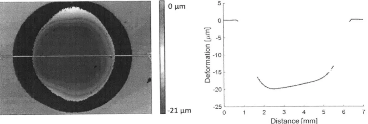
Figure 25: White light interference image showing the characteristic flat shape of the epoxy contracted membranes. A 6 mm membrane is shown here. The shape is not perfectly level due to imperfect settling of the glass cap. At the edge of the membrane the slope is high enough that not enough light is reflected back to the microscope objective to register as a measurement. 51
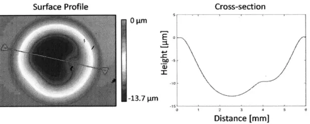
Figure 26: Deformation reliability for 6mm and 2.5mm membranes. 52 Figure 27: Surface profile (left) of a 6 mm membrane deformed using epoxy with two 400 pm ball
bearings added. The bearings are clearly visible in the surface map and the cross section (right). 53
Figure 28: Diagran showing the benefits of controlling the curved electrode shape. In the normal curved shape, the forces drop off rapidly away from the edge. In the controlled curvature shape, large forces are possible in the center as well. 54 Figure 29: Illustration of shorting paths for three potential devices. The isolation trenches surround the
diaphragm, isolating it from the wafer edge. Three designs are shown: no isolation (top), device layer isolation (middle) and complete device and handle isolation (bottom).
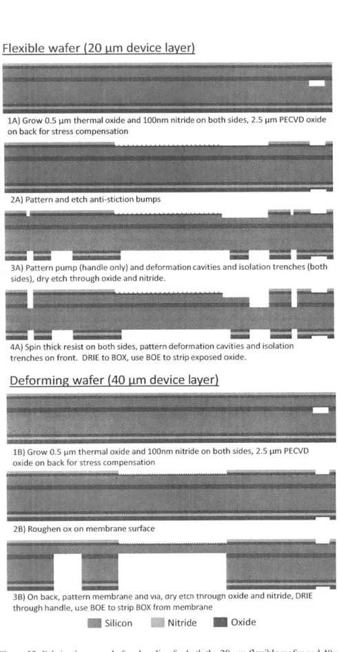
Figure 30: Top views of actuator design. The cleavage features were used for plastic deformation tests in 2.2.3, and are not used in these devices. (Left) Die schematic formed by overlapping masks. Anti-stiction bumps have been omitted for clarity. (Right) Top view showing a 10 mm diameter flexible membrane. The color variation on the membrane and via surfaces are due variations in the oxide thickness resulting from etch non-uniformity. 59 Figure 31: Cross-section of short loop electrostatic actuator design. 59 Figure 32: Fabrication steps before bonding for both the 20 pm flexible wafer and 40pm deforming
wafers. 60
Figure 33: Fabrication steps including wafer bonding and final DRIE etch. 61 Figure 34: Anti-stiction bumps were included on the deforming membranes to prevent stiction.
Variations in coloration between the two images are largely due to the angle at which the oxide is
viewed. 62
Figure 35: (Top) Processed wafers for electrostatic actuation tests. (Bottom) 10 mm diameter membrane
dies are shown on the bottom. 64
Figure 36: SEM image of the cross-section of a 2 mm electrostatic actuator. The upper membrane is the flexible layer, while the lower membrane has been plastically deformed. The device was initially
diced partially through the upper wafer, and then cleaved the rest of the way through. It is clear that the membrane edge is further out than expected, approximately 44 pm from this image. The larger
radius decreases the membrane stiffness and leads to slightly lower pull in voltages. This is
discussed further in Section 4.5.1. 65
Figure 37: Electrical layout for pull-in testing. The measurement resistor Rm allowed accurate
measurement of the voltage across the device 66 Figure 38: Repeated pull-in events with different voltages, demonstrating charge trapping in the
dielectric. Reversing the polarity restores the initial pull-in voltage. 67 Figure 39: Vacuum chamber used to test electrostatic actuators at reduced pressure. 68 Figure 40: Illustration of how grid pattern is reflected and distorted off of the actuator surface. 68 Figure 41: These images show the reflection off of a 5mm membrane with Weff = 15 pm, actuating in
vacuum. With no applied voltage (left), the grid pattern can easily be seen. Some initial bow due to the uneven oxide thicknesses causes the reflection to warp slightly. (Right) After applying the pull-in voltage the image becomes quite distorted. 69 Figure 42: H Bridge configuration using 4 optical relays. This circuit creates a square wave across the
device under test (DUT) of magnitude Vapp centered at OV. The control voltage, A = 5V, is a separate square wave that sets the switching frequency. 70 Figure 43: Square wave created by optical relays in H Bridge configuration. At higher frequencies above
-100Hz, the relays cannot switch fast enough to generate a sharp square wave. Actuation remained
below 10 Hz throughout testing. 71
Figure 44: Pull-in results from short loops. All results are from actuators have 6mm diameter, 20 pm
thick flexible membranes. 72
Figure 45: A comparison of the intended geometry (left) and the fabricated geometry for tested
electrostatic devices. 73
Figure 46: Pull-in voltages for electrostatic actuators with one plastically deformed electrode compared to the magnitude of curvature. These devices all have an effective gap (geff) of 0.43 pm. The effective gap is derived in Section 4.1 74 Figure 47: Pull-in voltages for electrostatic actuators with one epoxy contracted electrode compared to the
magnitude of curvature. These devices all have an effective gap (geff) of 0.23 pm. The effective
gap is derived in Section 4.1 75
Figure 48: Parallel plates under an applied voltage with a uniform gap (left) and a gap including a
dielectric layer (right). The upper plate is restrained by a spring with spring constant k. 78 Figure 49: Geometry for curved electrode actuation showing differential elements. The spacing between
upper and lower electrodes has been greatly exaggerated. 82 Figure 50: Assumed mode shapes are shown with increasing w compared to a curved electrode with a
shape defined by W = 1 - r22, which is a close approximation of the plastically deformed membrane shape. The curved electrode is shifted up slightly due to an assumed air gap at the edge.
89 Figure 51: Cartoon showing dimensions for plastic. deformation pull in calculations. The material in
black is oxide, blue is the lower deformed electrode, and orange is the upper flexible membrane. 91 Figure 52: Comparison of modelling results to measured electrostatic pull-in voltages. The predictions
assume a geff = 0.43 pm. 92
Figure 53: Variations in the effective air gap have a slight effect on the pull-in voltage. 93 Figure 54: Variation in pull-in voltage due to variability in the membrane diameter. 94
Figure 55: Dependence of pull in voltage on the device layer thickness. 95 Figure 56: Worst case scenario where all of the potential dimension variations combine to make the
membrane softer or stiffer. This shows the full range of expected pull in voltages due to device
variation. 96
Figure 57: Cartoon showing dimensions used for epoxy contraction pull in calculations. The material in black is oxide, blue is the lower deformed electrode, and orange is the upper flexible membrane. 97 Figure 58: Measured pull-in data (o) compared to predicted pull-in values (x). 98 Figure 59: Non-dimensionalized shapes used as curved electrodes. The dotted lines show where the
curves overlap. 99
Figure 60: Predictions of pull in voltage for the shapes considered. All electrodes are shown for both an effective gap geff= 0.5 pm (solid line) and geff=0.1 pm (dashed line), with a 6mm membrane.
100 Figure 61: Displaced volume compared to pull in voltage. Curves with lower pull-in voltages for a given
volume displaced are better for vacuum pumping. All electrodes are shown for both an effective gap
geff= 0.5 pm (solid line) and geff=0.I pm (dashed line). 101 Figure 62: A comparison of our predicted pump performance to the best performing commercial vacuum
pumps from Pfeiffer, Schwarzer Precision, KNF, Thomas, and Creare. 106 Figure 63: Diagram showing dead volume and pumped volume for a diaphragm actuator. Dead volume
includes all of the unpumped volume between the inlet and outlet ports on the left and right, while the pumped volume is the volume displaced during actuation. In this example, dead volume has
been increased due to a bubble trapped under the membrane. 107 Figure 64: Pictures of micropump. The internal pump features (top). The top side (showing electrical
vias) and bottom side (with fluid connections) are shown on the bottom. 109 Figure 65: (Top) The layout for a MEMS vacuum pump. The large circular membranes are the pump
chambers, while the smaller membranes are valves. There are eight circular vias that allow
electrical contact to the actuator layers. (Bottom) Cross-section (following the red path in the upper diagram) showing the critical features of the pump. 110 Figure 66: Surface map for membrane after pull-in, shown for 10 pin diameter anti-stiction bumps with
150 pm pitch under 6 atm of pressure (equivalent to 75 V across an effective gap of 202.6 nm. The domain modelled is 450 tm x 450 pm.
I
13 Figure 67: Deflection between anti-stiction bumps based on bump pitch. Estimated using COMSOL with6atm of pressure, equivalent to 75V across a constant gap of geff=202.6 nm corresponding to
1
00nm tall anti-stiction bumps. A fourth order polynomial best-fit line is shown, with R2 =0.999998. 114
Figure 68: Base pressures for the micropump design, shown for a 6mm diameter pump membrane. 115
Figure 69: Variations in plastic deformation magnitude and membrane radius, with the dead volume calculated from the micropump design (shown for a single pump stage). 116
Figure 70: Proportion of dead volume from four major sources: space around anti-stiction bumps after pull-in (both pump and valves), venting channels, and connection channels. The dead volume is independent of the curved electrode shape. 117
Figure 71: All of the air leaving an actuator must pass through the outlet venting channel. If it is the same
size as the other channels, it will reduce the flow out of the device. 118 Figure 72: A ZYGO white light interference microscope measurement of a 3mm electrostatic actuator
(no applied voltage). The effect of 4 pm deep venting channels is clearly visible on the lower left 10
side of the electrode surface. The membrane shown is 20 pm thick, and a 0.5 pm oxide layer on the surface is causing the curved surface. 119 Figure 73: Base pressure predictions for several membrane shapes, using the dimensions from a recent
micropump design. The defonnation magnitude, Wmax, is 25 prm for all calculations shown. The plastically deformed and cone shapes have the same volume, and thus the same base pressure. 121 Figure 74: Comparison of pull-in voltage to base pressure for several curved electrode geometries.
Additional dead volume was added to the flat electrodes because parallel plates do not pump all the
way to the edge. 122
Figure 75: Comparison of pump rate with frequency ramping (left) and constant cycle times (right). For this calculation, the pump was evacuating a
1 cm
3volume. Previous work [11] found a leak rate of
3xI0~3 sccm across the pump valves. 125
Figure 76: Steps for efficient venting of a diaphragm pump with two diaphragm valves. (Left) air fills pump chamber from the open inlet valve. (middle) The pump chamber is compressed until the pressure reaches I atm. (Right) The outlet is opened and the pump chamber vents out. 126 Figure 77: Two compression schemes are plotted here. (Left) Pump chamber remains sealed and
compresses the air from (VI, P1) to (V2, P2) isothermally. (Right) The pump chamber compresses up to I atm, then vents the air without further pressure increase. 126 Figure 78: Thermodynamic work done by a diaphragm pump with 0.141mm3 pumping volume and 4.59 x
10-3 mm3 dead volume, corresponding to a 6mm diameter, 25 jim deep plastically deformed membrane. (Left) Calculations using frequency ramping to improve flow rate. Base pressure reached after about 600 s. (Right) Calculations assume a constant
1
Hz actuation frequency. Basepressure reached in about 30000 s. 127
Figure 79: Comparison of power consumption with other commercial vacuum pumps. 129 Figure 80 - Deformation cavity mask, with 150mm wafer outline (left), with a callout to an individual die
(right). 141
Figure 81 - Pump membrane and cleavage line mask, with 150mm wafer outline (left), with a callout to
an individual die (right). 142
Figure 82 -Venting Channel Mask, with 150mm wafer outline (left), with a callout to an individual die
(right). 142
Figure 83: Electrical via mask, with 150mm wafer outline (left), with a callout to an individual die (right).
143
Figure 84 - Electrical isolation mask, with 150mm wafer outline (left), with a callout to an individual die
(right). 143
Figure 85: Anti-stiction bump mask, with 150mm wafer outline (left), with a callout to an individual die (right). Bumps are 10 ptm across with a pitch of 35 pm. 144
List of Notation
(r, 0, z): position in cylindrical coordinates
(x, y, z): position in Cartesian coordinates
V4: biharmonic operator, (V4= V2V2
)
a: angle at edge of plastically deforming membrane
SW: virtual work Su: virtual displacement
APfOW: pressure difference due to flow stress
,o: permittivity of free space (8.854 F/m)
Ei, E2: relative permittivity of material I or material 2
Ejj: strain : strain rate
K: system stiffness
2: nondimensionalized forcing term
;lj: critical forcing term resulting in pull-in [: viscosity
v: Poisson's ratio
p: material density
Pe: electrostatic pressure (F/A)
cr: flow stress
q0,9: normal stress in circumferential direction cij: stress on i face in j direction
ui'j: deviatoric stress, ai'j = aij - Ia
amax: largest absolute stress in body
arr: normal stress in radial direction
frO: shear stress in r-O plane a,: ultimate tensile stress ay: yield stress
T : pumping cycle time
-r: shear stress
<pj: mode shapes for displacement approximation a: membrane radius
A: area of electrostatic actuator c: air damping
C: capacitance
d: depth of anti-stiction bumps
D: flexural rigidity, D = Et3/(1
- v2) E: Young's modulus
Fe: electrostatic force
Fe(iw): electrostatic forcing finction
fi:
body force in ith directionF: spring force
g: electrode gap
geff: effective gap
h: height from neutral axis (h = t/2)
H(r): Heaviside function or unit step function
k: Boltzmann constant (1.381 J/K) k: spring constant
kerr: system stiffness, including electrostatic spring softening Kn: Knudsen number
m: anti-stiction pump period
ni: normal vector in ith direction
nrem: gas removed each pumping cycle
nleak: gas leaking in each pumping cycle
Pvacuum: base pressure of a vacuum pump PO: ambient pressure, usually 760 Torr P1, P2: pressure at state 1 and state 2
q: distributed load qe: charge
Qleak: leak rate
f: non-dimensional radial coordinate
R: gas constant (8.314 J/mol-K) Rh: hydraulic resistance t: time t: membrane thickness t2: thickness of material 2 T: temperature T: membrane tension
T1, T2: temperature at state 1 and state 2 U: activation energy for dislocation motion
Uc: stored energy in capacitor
UPS: stored energy in power supply
ui: displacement in ith direction V: applied voltage
VO: initial system volume
V1, V2: volume at state I and state 2
Vcap: volume of spherical cap
Vd: dislocation velocity
Vieaa: dead volume
geom: volume derived from geometric constraints
vpumped: volume pumped in one cycle
Vpj: critical pull-in voltage
Vvent: dead volume due to venting channels
w: deformation
iv(f): non-dimensional membrane displacement is1: scaled displacement of mode shape
pi
PI,1: central deflection resulting in pull-in
was: maximum displacement between anti-stiction bumps w05: oxide bow
wmax: maximum deflection of membrane; Wmax = w(r)Ir=o wvent, hvent, Ivent: width, height and length of venting channel
W: shape of curved membrane
W: non-dimensional curved electrode shape
Wcombined: non-dimensionalized combined shape of epoxy and oxide Wepoxy: non-dimensionalized epoxy contraction membrane shape WE: external work
Weff: effective deformation magnitude
W: internal work
Wmax: curved deformation magnitude
zc: critical height for pull-in instability
z: deflection of pressurized membrane, while deforming zo: initial electrode height (gap spacing)
Chapter
1
Introduction
1.1 Motivation
Microscale sensors and transducers are becoming increasingly common in everyday life. Modem smartphones have many internal sensors, including inertial sensors, gyroscopes,
compasses, and miniature microphones. Inertial sensors also appear in applications as varied as guided munitions to satellites [I]. Many safety features of modern automobiles rely on
accelerometers and gyroscopes, such as the automatic braking system (ABS), electronic stability control, and crash detection for rapid airbag deployment [2]. Small pressure sensors can be embedded in the tire wall and wirelessly alert the driver to low tire pressure [2]. Full tires decreases rolling resistance and improved fuel efficiency. Long used in office projectors, DMD chips are now appearing in many other applications such as active headlights that direct light away from other drivers eyes [3], [4]. Mechanical resonators are used for applications as varied as filtering telecommunication signals for smartphones to providing a stable timing frequency for microchips [4]. Infrared cameras are usually composed of an array of miniature bolometers, which are sensors that absorb infrared radiation [5].
The functional elements of all of these devices are MicroElectroMechanical Systems (MEMS), which are small mechanical elements that move or vibrate based on electrical inputs. These devices are fabricated in a cleanroom using many of the same processes found in the
manufacturing of integrated circuits, enabling very small planar structures to be created with sub-micron precision. These techniques have enabled very precise, small, low power sensors to be created relatively cheaply.
Many of these sensors operate in a low pressure environment. MEMS switches and mirrors need low pressures to remove squeeze film damping effects. Vacuum enables them to move quickly without fighting air resistance. Accelerometers need low pressures to reduce noise from molecular motion. To sense the minute motions of the proof mass, very low pressures are required. Resonators and gyroscopes need low pressures to reduce air damping and increase quality factor. Thermal devices, such as bolometers or thermal actuators, need vacuum to remain thermally isolated from their environment.
Low pressures in the devices mentioned above is enabled by packaging the chips in vacuum at the foundry. This is only possible when the device is self-contained or the signal being sensed can pass through the walls of the package. Radiation (such visible light for mirrors or infrared radiation in bolometers) can pass through transparent windows. External forces and motion
(accelerometers, gyroscopes) can pass through the package by shaking an internal proof mass. Electrical signals required for most devices (resonators. switches, actuators) can pass through a sealed package through vias or wire bonds.
However, there are many potential devices that are not currently feasible because they require active vacuum pumping to operate. Consider mass spectrometry, one of the cornerstones of chemical analysis. This tool ionizes small amounts of a material and subjects the ions to electric and magnetic fields. The time of flight varies based on the particle properties, and ions are separate by mass to charge ratio and measured. Many molecules can be identified this way, making this technique critical to fields as varied as environmental monitoring, chemical weapons detection, food safety and disease diagnosis [6].
Unfortunately, there is not a portable mass spectrometer. This is often the case in portable analytics. Mass spectrometer [6], [7], gas chromatographs [8], [9], and many other chemical sensors both to need both a low pressure sensing environment and a method for bring the chemicals inside the device. This means that they cannot have a hermetic seal, and must have some method of active pumping to bring the pressure of the sensor down internally. Currently, it is possible to scale the sensors down to fit in a backpack [6], but for a truly portable chemical sensing platform, a small, low power vacuum pump is required.
The main reason that small vacuum pumps have not been successful yet is that it is very challenging to achieve a large compression ratio (for a displacement pump, this is the ratio between pumped volume and unpumped "dead" volume) in a small device. It is difficult to find an actuator that combines low power with high pumping volumes and minimizes dead volume. This thesis will argue that curved electrostatic actLlators provide a way to meet all of these
criteria and cottld be an enabl ing technology for mn iaturized vacuum ptumping. Electrostatic
actuation is inherently not dissipative and thus low power. The curved electrode increases the size of the pumping volume, and careful device design can minimize the dead volume.
Curved electrostatic actuators would be useful for many other applications. Using curved electrodes provides a way to generate large displacements with low voltages and power dissipation. This could be useful for a wide range of microscale devices that are currently
limited to the narrow gap between parallel electrodes.
1.2 Previous Work at MIT
Work on a MEMS vacuum pump began with a displacement pump developed Vikas Sharma's vacuum pump [10]. The pump was developed for the Micro Gas Analyzer project. The design was a displacement pump consisting of three elements: one large piston for the pump chamber and two smaller pistons for the valves. The pistons were thick pieces of silicon attached by flexible tethers to the rest of the substrate. The device was actuated pneumatically by applying
pressure or vacuum to the external side of the pump or valve. This device was able to achieve a base pressure of 502 Torr.
This initial pump provided proved that this basic design could be used to create vacuum, and pointed to several areas for improvement. Hui Zhou continued to develop the pump for the Chip Scale Micro Vacuum Pump program [11]. The new pump was still actuated pneumatically, but design improvements allowed the pump to reach a base pressure of 164 Torr [12]. At the time, it was the lowest base pressure for any micromachined vacuum pump. The design increased the pump stroke and decreased the dead volume in order to reach lower base pressures.
Additionally, Hui improved upon the valve sealing to decrease the pump leak rate.
The initial pump created by Vikas was quite large: 50 mm x 30 mm x 2mm (3 cm3). The second generation device built by Hui was significantly smaller, at only 1.14 cm3. However, both of these pumps required an external source of pneumatic actuation. This was very helpful for testing a proof of concept device, but it limits the pump to laboratory testing. In order to create a truly portable system, the next generation of the pumps need to have integrated actuation.
1.3 Curved Electrostatic Actuators
Several qualities are desired for integrated actuators. These are:
1. Small size: The solenoids and motors that drive many commercial pumps consume most
of the device volume. For a truly portable pump, smaller actuators are desired.
2. Low power: The more power the pump consumes, the larger the power supply needs to be.
3. Easy integration: A reasonable actuator must be easily integrated into standard cleanroom processing techniques.
4. Large volume displacement: In order to reach low pressures, pumps need to be able to achieve large compression ratios. For mechanical displacement pumps, this can be done by increasing the pumping volume and decreasing dead volume.
In this next section, it will be shown that electrostatic actuation with curved electrodes can meet all of these criteria.
Electrostatic actuators operate by applying an electric potential between two electrically isolated conductive surfaces. As the surfaces charge up, the electric charges create an attractive force between the two objects. The electrostatic force (for parallel plates) is given by:
__OA (1.1)
Fe = 2g 2
where E is the permittivity of free space, E is the relative permittivity of the medium between the electrodes, A is the area of the electrodes, and g is the gap between the electrodes. This is a highly nonlinear force that is much larger in regions with a narrow gap.
Electrostatic actuation is common in MEMS because it provides a simple way to apply forces and transduce signals without the need for transduction to other physical domains (such as thermal, piezoelectric, etc). Power usage is very low because the actuator is essentially a large capacitor; it stores most of the applied energy during actuation, and releases it again when the applied field is removed. There is no dissipation other than small resistive losses due to the displacement current.
When the gap between the conductors is small, the forces generated can be quite large. However, the nonlinear relationship to the gap (g) means that electrostatic force drops off precipitously when the gap is large. This means that electrostatic actuation is not well suited for
large stroke actuators with a constant gap.
Electrostatic actuators, in geometries as varied as such as cantilevers, comb drives, or diaphragms, tend to be flat and fabricated in the plane of the substrate. This is because the
structural layers are either intrinsic to the starting wafers or deposited on a flat wafer surface. One common method for forming devices starts with a Silicon-on-Insulator (SOI) wafer. These
wafers consist of a three layer: a thick silicon base layer called a handle, a dielectric layer (usually oxide), and a thin upper silicon layer called the device layer. If the insulator is oxide, the insulator is referred to as the Buried OXide (BOX) layer. Small, thin shapes, such as cantilevers, can be etched out of the device layer and released by etching away the BOX layer. These structures can be actuated laterally in the plane of the wafer. However, larger structures, such as diaphragms, cannot be cut out vertically. They must be formed by stacking layers on the surface of the substrate and removing a sacrificial layer. For this reason, larger structures tend to only be found with constant gaps between the plates.
Zipping provides a way out of the tradeoff between large forces and large displacements by introducing a variable gap height. For cantilevers, it has been demonstrated that by creating one curved electrode, pull-in can propagate along the beam at much lower voltages than for
comparable flat beams [13].
A similar technique can be used to zip a membrane down onto a curved electrode, generating large forces and displacements. The curved shape creates a variable gap, with a narrow air gap at the edge and a much wider gap in the center of the membrane. For our geometry, this means that there are large forces near the edge of the membrane, pushing the edge down. This creates adjacent areas with narrow gap, causing the membrane to "zip" from the edge to the center.
Because the force is nonlnear, at a critical voltage the membrane will snap down completely. This is called pull-in, with the critical voltage being the pull-in voltage. This process is shown in
Figure 1.
V=0 SV. <VUIw in vpulin *\ * 0.'1
Figure I: Stages of zipper actulation for a circular membrane above a rigid curved electrode (shown in cross-section).
With no voltage applied tie upper electrode is flat (top). When a voltage below the critical pull-in voltage is
applied, the mcmibrc dispilcs, w ith contact starting near the edges (middle). When the critical pull-in voltage is reached, the flexible mcmblrane snaps down onto the lower electrode (bottom). The black bumps represent anti-stiction bumps etched into tie insUlating oxide between the two electrodes. These bumps prevent the surfaces From sticking togcther.
Using a Cirved electiode has significant benefits both lor dLchiuving low pressures and for ptim ping at low voltages.
First, consider the electrostatic properties. The variable gap allows us to reach the pulIl-in instability at a much loXw'er critical voltage than if wx e used parallel plates with comparable spacing. A full anaiysis of parallel plates versus different curved geometries is presented in Section 4.6.
Now consider the curved actuator as a pumping element. The curved shape allows the
membrane to displace a much larger volume of air than comparable parallel plate actuators. The curved electrode can be mtich deeper than a comparable parallel plate electrode and still have lowx voltage pull-in. Additionally. the smooth surfaces between the two membranes mean that they wNill contact conformallv, waith very few air pockets. This limits the dead volume betwveen
We can place several of these actuators in series together to create a diaphragm pump. By actuating these membranes in the correct order, we can move air from the inlet (device) side to
the outlet (atmosphere). The cycle is as follows:
1) 2) 3) 4)
Start with all the membranes closed Open the inlet valve and pump chamber Close the inlet valve
Open the outlet valve and close the pump chamber
These steps can be repeated shown in Figure 2.
1. All closed
2. Air pulled
in
to create vacuim on the inlet side. A diagram of this process is
(device) (atmosphere) Inlet Outlet Ito, tnp
- 2
3. Close inlet 4. Air pushed out : w. N Nt N5 - N - .3Figenac 2: Method 'or creating v aCLium using a di aph ragm pum p, shown XVWith curved pump chamber and valves.
13lack bumnps on lower surface arc intended to preveni stiction between surfaces.
To create low pressures, the pimp membranes need to displace as much volume as possible. Conversely, the valves only need to actuate lar enough to allow air to flow through them, so the curved electrode for the valves can be much shallower.
1.4 Thesis Outline
The focus of this thesis will be on developing methods for integrating curved electrostatic actuators into MEMS devices, specifically vacuum pumps. Two methods for creating curved membranes, high temperature plastic deformation and epoxy induced contraction, will be discussed in Chapter 2. Deformation results will be presented along with a model for predicting the extent of plastic deformation. Chapter 3 presents methods for integrating these curved diaphragms into simple electrostatic actuators and testing the resulting devices to find the pull-in voltage. Chapter 4 describes a first order model for estimating the pull-in voltage for curved electrodes, and compares the predictions to experimental results. The performance of other curved electrode shapes are compared as well. In Chapter 5, the performance of a diaphragm pump utilizing curved electrostatic actuators is analyzed. Factors that affect the dead volume are considered in depth. Estimates of the base pressure are compared for a variety of curved
electrode shapes. The contributions from this thesis as well as future work are discussed in Chapter 6.
Chapter 2
Creating curved silicon membranes
2.1 Summary of curved electrode literature
There are several examples in the literature of other microsystems incorporating curved
electrostatic actuators. In this section, several of them will be described in more detail. Selected diagrams and figures from these examples are shown in Figure 3.
Branebjerg and Gravesen created an early curved electrostatic electrode with a similar geometry to our plastically deformed membranes [14]. A silicon membrane was bonded to a glass plate to form a cavity, and a pressure was applied between the two electrodes to push out the membrane. Applying a voltage between the silicon membrane and gold layer on the plate causes the
membrane to pull in and contact the plate. While the voltages achieved are low, a pressurized electrode makes this design less useful for vacuum pumping applications.
Jeahyeong Han et al. created a diaphragm flow pump using curved circular electrostatic actuators
[15]. The curved electrode was created using a dimpling machine with a diamond slurry to
create dimples in the silicon substrate, followed by CMP to smooth out the surface roughness. While their device was optimized for fluid flow rather than vacuum generation, this method could provide another alternative for making curved electrodes in a vacuum pump.
Resist reflow can be used to create curved structures as well. The lower electrode was formed by depositing a LPCVD film on a silicon wafer, then etching through the substrate to release the membrane. Resist is patterned on top of the membranes, and then exposed to hot solvents to cause the resist to reflow into a curved profile. Using gold as a seed layer, nickel is electroplated on top of the resist to form the upper electrode. Using this method, Yee et al. fabricated
microphones using an electrostatic actuator with one curved electrode, perforated for air flow [16], [17]. The curved electrode lowered the pull-in voltage significantly: for a 1.3mm square actuator, the pull-in voltage decreased from 337V for a flat electrode to 240V with a curved electrode (with comparable spacing between the electrodes).
Wagner et al. created an electrostatically actuated microvalve where both the lower and upper electrodes were curved [18]. Silicon dioxide on the upper electrode caused the membrane to buckle. The lower electrode was formed either with an isotropic wet etch or using grey-tone lithography. Isotropic etches form hemispherical cavities, which are not ideal for electrostatic actuation for several reasons. Formation of curved structures depends on a carefully timed etch; variations in timing can lead to different cavity sizes and depths, and thus variable actuator performance. Additionally, the edge of the etched cavity has a sharp edge, which increases the
voltage for pull-in. Grey tone lithography can produce arbitrary resist profiles across a wafer, and transfer these shapes into the underlying substrate using an reactive ion etch (RIE) [19]. To do this, the features on a standard quartz/chrome mask are broken into square pixels, and the size of each pixel is modulated to control the amount of light that reaches the resist for exposure. Light from adjacent areas blur together; after developing the pattern, resist is left with height proportional to the size of the pixels. However, the process must be carefully calibrated to match the grey scale exposure time and RIE resist selectivity in order to create the desired geometry. McIntosh et al. created pressure sensors utilizing curved trench electrodes [20]. The electrode curvature enabled them to create a sensor with a linear capacitance to pressure relationship over a large range. They used an electrical discharge machine (EDM) to cut curved trenches in glass wafers, and anodically bonded a flexible silicon membrane to form the upper electrode.
DRIE (Deep RIE) is known to have variable etch rate, known as DRIE lag, depending on feature size and density. This normally leads to undesirable nonuniformity, but it can also be used to make variable curved geometries. Chou and Najafi [21 ]created very tightly spaced trenches with varying widths, utilizing DRIE lag to etch them to varying depths. A subsequent isotropic etch (wet or dry) removed the walls between the trenches and smoothed the curved feature. This process can create arbitrary geometries, but requires a careful characterization of tool and feature
dependent DRIE lag.
~''T'TT'''
S Vkibl.ic w,(inuluctin' diaphraign
An k~CtndwC) -1t IrIteCrx ~1t V2ihc di Foot Back d /
(
nenbran. / 4/ .. .... ... . mnembrane iragrn gap r.2 tFigure 3: IE xamplcs o curved electrodes in the 1 iterature. a) BrIanebjer and Graveson [1 4 h) JcahvyeoiIn Han et
a. [15], c) Sc ciw aL 116], d) Wagner et al 18], C) McIntosh c al 1201, ) Chon eS al. (image shown elore
isotropic etch smooths surface) [2 I
2.2
1-igh Temperature Plastic Deformation
Many materials exliit elastic plastic delormation behaior. This means that under small loads it behaves elastically, and will return to their original state
Once
unloaded. Above a critical stress, called the yield stress (a,,). the material will start to permanently cie'orm. The permanentde lormation is called plastic de lormation.
The ultimate tensile strength (on) ofa material is the maxirmum amount of stress that a material can withstand beore breaking. Ductile materials dclorm plastically before reaching a,. Brittle
materials, like silicon, crack and Cial at cYU Vithout any plastic deltrmation. Another way to think about this is that the ultimate tensile strength is reached belbre the y icid stress. [ lowever,
at elevated 'emperaturcs, the yield stress drops. At high en1-gh temperatUres, Siicon beCOmes ductile and can plastically delOrm before reaching the
fracture
stress.24 b Vah C d it C 57.
K
Unlike ductile metals, above the yield stress, single cry stal silicon has a much lower flow stress
Jf. This means that once silicon starts to deform, much less stress is required to continue straining the material than was required to reach yield. An example of this constitutive relation is shown in Figure 4.
10
0 0 125
-Yield stress (y)
100 Gy 10 21Lr n~ 2 75 C,)) Flow stress ((T 2s 0 I I I 10 0 2 4 6 500 600 700 600 900 1000 1100 Percent Strain Temperature [SC]
Figzure 4: Above 600 "C, the yield stress for silicon is below the fractUre stress, and the material can start to flow. As the temperature rises, the yield and flow stress drop. (Left) Data taken from [23] with a calcUlated best fit line. (Right) Plot adapted from [23], showing constitutive behavior for dislocation free silicon at 8 15 "C with a crosshead displacement rate of 5x 10- cm/mmn.
Some planes in a crystal, called slip planes, have less resistance to motion. When a crystalline material plastically deforms, the slip planes start to slide past one another. Even in these preferential directions, the crystal does not slide all at once. Breaking all the bonds at once and reforming them in the new position would require a massive amount of energy. Instead,
dislocations, or defects in the normally ordered structure of a crystal. allow individual bonds to break and reform, allowing crystal planes to flow past each other one atom at a time.
Both the flow stress and yield stress have been shown to be of the form [24]:
T OC
O P'exp(U
(2.1)where r is the resolved shear stress along the dislocation's direction, t is the strain rate, ii is an experimentally determined fitting parameter, U is the activation energy for dislocations, and k is the Boltzmann constant. This expression shows that the flow stress and yield stress increase with larger strain rates, and decrease at elevated temperatures. These properties have been carefully
measured [23], [24] and modelled [251.
Since the annealing process slowly heats at -5 "C/min, the load is applied gradually. This means that the membranes will strain slowly. If the strain occurs uniformly over the ramping process. the largest strain rate experienced by any device would be 1.67 x 10- cm/min. For our
predictions, we will be using Uf and a, measured with t = 5x103 cm/min [23], the lowest strain
rates available, even when our strain rate was actually lower. At high strain rates, variations in i leads to large changes in the flow and yield stresses, but at lower strain rates the changes are smaller. For this reason, it is reasonable to use cf and ay 5x] 0-3 cm/min, even though it is larger than the expected strain rate.
The yield and flows stresses are very sensitive to the concentration of dislocations in the material. The velocity of each dislocation is proportional to the applied shear stress [26]:
V OC TM (2.2)
where Vd is the velocity of the dislocation. At low dislocation densities, plastic flow is limited because only a few dislocations exist. At a constant strain rate, to achieve an incremental displacement each defect must move further. This requires larger stresses to create the necessary dislocation velocities (2.2). As the material deforms, additional dislocations are created and the velocity of individual dislocations drops. This causes the stress needed for further straining to decrease. Eventually enough dislocations have formed that they start to interfere with each other, decreasing the benefit of higher dislocation densities, and the stress needed flattens out
into the flow stress (cf). Dislocations themselves create a localized stress strain field. Once enough of them have formed, these fields inhibit further plastic flow, and the flow stress starts to
increase again. This is called stress hardening.
2.2.1 Summary of Deformation Process
By controlling the location and magnitude of the applied stress, the deformation in the silicon can be used to create a variety of curved structures. Several examples of this exist in the
literature. Selected diagrams and figures from these examples are shown in
Large parabolic "parasols" for use as X-ray lenses were formed be pressing a curved quartz mold into a silicon wafer [27]. Scanning micromirrors supported on thin tethers were permanently rotated around their supports. This was done by applying a load to the edge of the mirror at elevated temperatures in a furnace [28] and using localized resistive heaters [29]. When actuated, these out of plane comb drives rotated around the pivot point. Cantilevers and
membranes can be bent out of the wafer plane by applying a load to the end of a cantilever [30],
[31].
Most relevant to the current work is the research by Huff [32]. He used plastically deformed membranes to create a pressure control switch [33] and developed a model to predict the extent of plastic deformation in circular silicon membranes [34]. We will build on his work in the
following chapter.
ci
~)I
b .. ... C I i14 '4 f cSI Swith OpenFigure 5: Examples of devices created using high temperature plastic deformation of silicon. a) Aono et al. [271,
b-c) Jongbaeg ct al. [28], [29, d-e) Frthauf et al. [301I [3 1], F) Huff [331.
The devices modelled in this section are cirCLilar membranes that are plasticall\ deformed during xaelcr bonding. A precise volume is etched into the device layer of an SO wafer (henceforth referred to as the deformation volume and deformingz wafer). A circular membrane is formed by etching. through the handle xvafer. The deforming wafer is contacted in a nitrogren environment
to another wafer. During the high temperature anneal that fuses the wafers together, the N, expands, pressurizing the membrane and causing it to plastically deform. The expansion of the membrane decreases the pressure, lowering the stress and causing the deformation to terminate at the desired magnitude.
These steps are shown in Figure 6. A more detailed process for device, Section 2.2.3.
Deformation cavity Membrane
1. Pattern lower wafer to form membrane and deformation volume
2. Align and contact wafers in N2at 1 atm.
3. Anneal bonded pair at high temperature to deform
Figure 6: Basic steps for creating plastically deformed membranes. The blue layer is the device layer of an SOI waler.
2.2.2 Modeling plastic deformation
In
this section a model will be presented that predicts the extent of plastic deformation fora
circular membrane
undergoing
a high temperature anneal \\with a defined volume of air on the back side.First, a ew assumptions are necessary about the constitutive relationship of the deflorm 11ng
material.
Silicon is a material \with cubic sy mmetry. This means that three independent stiflness
components are needed to completely describe elastic behavior and the plastic yield depends on the orientation of the applied stresses. Material properties, such as Y oung's modulus (F). vary
w idely with direction: E has a maximum of 188 GPa in the <I l> direction and a minii mum of
I130
Ga in the <100>
direction.I low ever, we only need to consider the material properties in the plane of the delorming mem brane because the diaphragm is thin enough to be in plane stress (u3i = 0). For a 100
wa Kr, with in the plane F ranges from
130
GPa in the <100 direction to 169 G1a in the <1
0>direction. Poisson's ratio ranges from v = 0.064 in the <110> direction and v = 0.28 in the <100> direction [35].
To simplify the analysis, we will assume that the material behaves isotropically with a Young's modulus (E) and Poisson ratio (v) of 150GPa and .17, respectively. This is the average value for both parameters in the plane of the membrane, and it will be seen that this approximation
provides a reasonably fit for the experimental data.
If a crystal starts with a significant dislocation density, the initial yield stress can be depressed. In cases with very high dislocation density, the yield stress ay can disappear entirely, allowing the membrane to flow as soon as Uf is reached. RIE etches can cause damage (and create dislocations) on the surface [36]. For our devices, all etches stopped on an oxide etch stop and did not directly etch the silicon device layer. For this reason it is believed that the starting wafers
had a low dislocation density, but without knowing the effect of processing steps, both defect
free (high ay) and high defect density (ay = af) will be considered.
Predicting the extent of plastic deformation is done in two steps. First, the elastic response is calculated to determine the stresses in the membrane. If stresses satisfy the yield criterion, then
the magnitude of the pennanent plastic deformation is calculated. Otherwise, the membrane does not deform.
First, consider the elastic response. As the temperature rises, the gas inside the membrane expands and the pressure increases. For a circular plate under a uniform load, the shape of the membrane is:
w(r) = q (a2
-r2)2 (2.3)
64D
where q is the pressure load, D = Et3/(1 - v2) is the flexural rigidity, and a is the membrane
radius. It should be noted that q is not the absolute pressure inside the membrane, but the difference between internal and external pressures. (2.3) can be integrated to find the volume due to the pressurized geometry.
7Tn q2a 2n (2.4)
V eom = az 2D] azwinax
where Winax = w(r)|r-o is the maximum deflection of the membrane. Thermodynamics provides another equation for the volume. From the ideal gas law,
= P1 T2 (2.5)
P2 T1
P1, V and T1 are the initial conditions, and T2 is set by the annealing temperature.
Thermodynamics must agree with the geometric volume, so we can set equations (2.4) and (2.5) equal to each other and solve for P2 and V2. Using this final pressure, we can calculate the