HAL Id: cea-01615818
https://hal-cea.archives-ouvertes.fr/cea-01615818
Submitted on 12 Oct 2017
HAL is a multi-disciplinary open access
archive for the deposit and dissemination of
sci-entific research documents, whether they are
pub-lished or not. The documents may come from
teaching and research institutions in France or
abroad, or from public or private research centers.
L’archive ouverte pluridisciplinaire HAL, est
destinée au dépôt et à la diffusion de documents
scientifiques de niveau recherche, publiés ou non,
émanant des établissements d’enseignement et de
recherche français ou étrangers, des laboratoires
publics ou privés.
Towards contact integration for III-V/Silicon
heterogeneous photonics devices
Elodie Ghegin, Philippe Rodriguez, F Nemouchi, Ch Jany, M. Brihoum, A.
Halimaoui, I. Sagnes, B Szelag
To cite this version:
Elodie Ghegin, Philippe Rodriguez, F Nemouchi, Ch Jany, M. Brihoum, et al.. Towards contact
integration for III-V/Silicon heterogeneous photonics devices. 2016 IEEE International
Intercon-nect Technology Conference / Advanced Metallization Conference (IITC/AMC), May 2016, San Jose,
United States. pp.69 - 71, �10.1109/IITC-AMC.2016.7507684�. �cea-01615818�
Towards contact integration for III-V/Silicon
heterogeneous Photonics devices
E. Ghegin
1,2,3, Ph. Rodriguez
2, F. Nemouchi
2, Ch. Jany
2, M. Brihoum
2, A. Halimaoui
1, I. Sagnes
3, B. Szelag
21 STMicroelectronics, 850 rue Jean Monnet, 38926 Crolles Cedex, France.
2 Univ. Grenoble Alpes,
F-38000 Grenoble; CEA, LETI, MINATEC Campus, F-38054 Grenoble, France.
3 CNRS-LPN,
Route de Nozay, 91460 Marcoussis. Contact E-mail : [email protected]
Abstract—Silicon photonics is of great interest as it opens the
way to large bandwidth and high data rates. A pioneer Silicon photonics scheme consists in integrating III-V lasers on the SOI substrates containing the passive components. However, key developments are necessary to co-integrate III-V devices with CMOS very large scale integration (VLSI). In this paper we propose a CMOS-compatible integration scheme of contacts (i.e. semiconductor metallization and plug) on III-V surfaces taking into account the limitations fixed by the operating laser device. Based on metallurgical, morphological, optical and electrical studies, processes are submitted and reviewed for the purpose of forming stable and reproducible contacts with low resistivity in a 200 millimeters fab line.
Keywords—Silicon Photonics, Heterogeneously integrated III-V laser on Silicon, Contact integration
I. INTRODUCTION
Allowing data rates beyond what electronic component can offer Silicon Photonics have been identified as one promising paradigm. However, while silicon is of huge interest for the making of passive components, its indirect band gap prevents it from being an efficient light emitter. As a consequence, the making of the photons’ source requires the use of different materials. An innovative solution consists in integrating III-V lasers on SOI (Silicon on Insulator) substrates which support the passive components such as the waveguide (Fig. 1) [1], [2]. To produce such a pioneer device, one of the most critical developments relates to the integration of the contacts that are key to electrically pump the III-V laser. Indeed, in current Photonics devices the III-V laser is external and coupled to the passive components thanks to an optical fiber. The contacts present on these external lasers are comprised of Pt, Pd or Au multilayers and based on a lift-off integration [3], [4], [5]. Such a scheme is not conform to the “on-SOI-integrated-laser” standards. In order to fulfil the Silicon Photonics requirements, the innovative contacts (i.e. metallization and plug) on n-InP and p-InGaAs must:
- be integrated thanks to 200 millimeters front-end compatible processes which exclude any lift-off or related processes;
- be comprised of front-end compatible materials only, such as Ni, Ti and their alloys;
- be feasible at low thermal budget (T < 450 °C) in order not to degrade the active region of the laser composed of multi quantum wells (MQW);
- present a contact resistivity lower than 10-6 Ω.cm2. A higher contact resistivity would cause a local heating that may give rise to a wavelength shift of the produced photons.
Fig. 1: Schematic representation of a III-V Laser integrated on an SOI substrate which supports the passive photonics components in the frame of Silicon Photonics
In this paper, we review and evaluate the various technological solutions for integrating contacts that meet the previously listed requisites.
II. CONTACTS INTEGRATION SCHEME
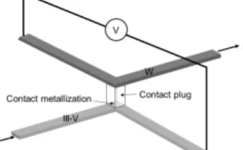
To identify the most relevant processes and to develop them, morphological and electrical test vehicles such as transmission line model structures (TLM) and cross bridge kelvin resistors (CBKR) were integrated either on n-InP or on p-InGaAs surfaces (Fig. 2).
Fig. 2: Schematic representation of a cross bridge kelvin resistor (CBKR) used for the acquisition of I(V) characteristics and for specific contact resistivity extraction
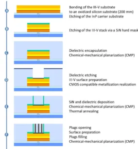
Two inches III-V substrates were reported on 200 millimeters silicon substrates enabling the processing of the wafers in an industrial 200 millimeters fab line. The process flow related to the proposed and reviewed integration is schematically shown in Fig. 3.
Fig. 3: CMOS compatible process flow for the integration of the contacts on a III-V epitaxy in the framework of Silicon Photonics
III. DETAILED DESCRIPTION OF THE PROCESS FLOW
A. Transfert of the III-V stack on the silicon substrate
The III-V wafers are transferred on oxidized silicon wafers thanks to a direct bonding process and the III-V carrier substrate is etched up to the active layers, i.e. n-InP or p-InGaAs as displayed in Fig. 4.
a) b)
Fig. 4: Picture of a 2 inches III-V substrate (a) after its bonding to a 200 millimeters oxidized silicon substrate and (b) after the etching of the III-V carrier substrate
B. Ecthing of the III-V stack via a SiN hard mask
The etching of the III-V stack requires the use of a SiN hard mask which deposition temperature and intrinsic stress must be kept as low as possible (i.e. T ≤ 300 °C and σ ≤ 100 MPa) in order not to deteriorate the III-V surfaces on which the contacts will be integrated. The inductively coupled plasma process (ICP) used for this III-V etching provides high etch rates and leaves smooth and vertical sidewalls (Fig. 5). Note that when reporting full two-inch substrates a great surface of the expensive III-V stack is lost during the etching. In order to minimize the material loss, a solution consists in bonding millimeter-scale dies on the SOI substrate thanks to dedicated holders before the etching step.
Fig. 5: FIB/SEM image of a III-V stack after its dry etching via a SiN hard mask. Note that the TEOS and W were used for the FIB etching only.
C. Dielectric encapsulation
In order to electrically isolate the contacts regions, the whole structure is encapsulated by a dielectric compound. The choice of the dielectric nature is crucial because of its vicinity from the laser’s active region in the device. A low transmittance of this material at the laser wavelength would cause unwanted optical losses; a low thermal conductivity (σ) wouldn’t enable a proper evacuation of the heat produced by the operating laser. 0 20 40 60 Al2O3 SiO2 T h e rm a l c o n d u c ti v it y [ W /m /K ] SiN 78 80 82 84 86 88 90 92 94 96 O p ti c a l tr a n s m is tt a n c e @ 1 .3 -1 .5 µ m [ % ]
Fig. 6: Thermal conductivity and optical transmittance at 1.3-1.5 µm of
SiN, SiO2 and Al2O3
As indicated in Fig. 6, Al2O3 appears to be the best compromise for the laser encapsulation. Because of the present topography, a flattening of the surface must be made thanks to a chemical-mechanical planarization (CMP). The planarization of the Al2O3 being challenging, the deposition of stacks combining SiO2, Al2O3 and SiN was retained as the most adapted solution for the dielectric encapsulation.
D. Contact metallization
1) Cavities opening and III-V surface preparation
The opening of the cavities in the dielectric stack is one of the most sensitive step in this integration flow as it must not deteriorate the n-InP or p-InGaAs surface where the ohmic contacts will be formed. For this purpose, studies are being conducted to determine the most appropriate SiN etching process. The III-V surface being very reactive when exposed to oxygen, a two-step surface preparation is carried out to suppress contaminants and oxides. The first step consists in a wet surface preparation; the second in a plasma treatment. (i) We developed a scheme combining diluted HCl and Ar or He plasma treatments to remove oxides on InGaAs without inducing any morphological damage on these surfaces [6], [7]. (ii) We demonstrated that the preparation of InP surfaces is more delicate as concentrated HCl increases significantly its roughness by anisotropically etching it (Fig. 7). We also highlighted that an Ar preclean removes efficiently the oxides present on such surfaces but modifies their crystallinity and stoichiometry [6], [8]. On the contrary, diluted H2SO4 and HCl solutions combined with a He preclean seems to be a more adapted compromise for the preparation of InP surfaces (Fig. 7) [6].
Fig. 7: AFM scans of a InP surface (a) before and after a wet surface
preparation in (b) HCl:H2O (1:2) (c) HCl:H2O (1:11) (d) H2SO4:H2O (1:9);
The Root Mean Square roughness is (a) < 0.2 nm (b) 1.7 nm (c) < 0.2 nm (d) < 0.2 nm
2) CMOS-compatible contact metallisation
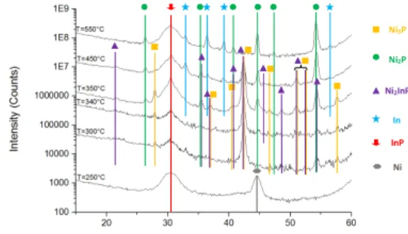
Two strategies can be followed for the formation of the CMOS-compatible metallization: (i) One can choose to deposit directly the metallization of interest on the III-V surface. The stabilization of the phase(s) is achieved by mean of an annealing process. (ii) One can also choose to deposit a metal and to perform a thermal treatment for the purpose of forming an intermetallic compound by solid state reaction with the III-V. Metallurgical studies were conducted on the Ni/InGaAs system and showed the formation of a unique hexagonal phase [9]. A similar study on the Ni/InP system underlined the appearance of various phases (Ni2P, Ni3P and Ni2InP) based on different applied thermal treatments and the formation of the In phase from 350 °C (Fig. 8) [8].
Ni2InP Ni2P Ni3P In Ni InP
Fig. 8: XRD patterns of Ni/InP samples annealed at 250 °C, 300°C, 340°C, 350 °C, 450 °C and 550 °C for 60 seconds (RTP). A 2° offset on the incident beam was applied in order to minimize the InP substrate contribution
The two contacts (i.e., on n-InP and p-InGaAs) being sequentially integrated in the laser device, thermal budget constraints have to be respected during the making of the second-stage contacts. The thermal stability of the Ni-InGaAs intermetallic was studied and exhibits strong restrictions (Fig. 9).
Fig. 9: Evolution of the sheet resistance in a Ni/InGaAs system after various thermal treatments and corresponding TEM pictures
E. , F. Metallization encapsulation and Plug integration
Subsequently to the dielectric stack deposition, cavities are opened and a surface preparation of the metallization is carried out. A diffusion barrier layer usually composed of CVD-TiN (Chemical Vapor Deposition) is deposited on the walls of the cavities. An alternative consists in depositing a CVD-F-less W which is of great interest for its electrical properties at low thicknesses (Fig. 10). This attribute opens the way for lowering the plug resistivity which is essential to minimize the overall resistance.
0 100 200 300 400 100 200 300 400 500 600 CVD - TiN CVD - W R e s is ti v it y [ µ O h m .c m ] Film thickness [Å]
Fig. 10: Resistivity of CVD-TiN and CVD F-less W as a function of the films thicknesses
Regardless the choice of the diffusion barrier composition, the cavities are then filled with W. A final CMP ends the integration of the CMOS-compatible contacts as represented in Fig. 3, step F.
IV. CONCLUSION
The integration of III-V lasers on SOI substrates appears to be a promising but challenging architecture for innovative Silicon Photonics devices. In this paper the main roadblocks towards contact integration requiring developments and key studies were clearly highlighted. Thanks to metallurgical, morphological, optical and electrical studies we were able to propose and develop schemes and processes opening the way to a CMOS-compatible contact integration on III-V surfaces.
ACKNOWLEDGMENT
The authors would like to thank B. Previtali, T. Card, N. Chevalier (CEA-LETI) and J. L. Lábár (MTA EK MFA) for their help during this study. This work was funded thanks to the French national program 'programme d’Investissements d’Avenir, IRT Nanoelec' ANR-10-AIRT-05.
REFERENCES
[1] B. Ben Bakir et al., “Heterogeneously integrated III-V on silicon
lasers,” Meeting Abstracts, vol. MA2014-02, no. 34, p. 1724, 2014.
[2] G.-H. Duan et al., “Hybrid III-V on silicon lasers for photonic
integrated circuits on silicon,” J. Sel. Top. Quantum Electron, vol. 20, pp. 158–170, July 2014.
[3] A. Baca et al., “A survey of ohmic contacts to III-V compound
semiconductors,” Thin Solid Films, vol. 308-309, pp. 599–606, 1997.
[4] A. Katz et al., “Au/Pt/Ti contacts to p-In0.43Ga0.47As and n-InP
layers formed by a single metallization common step and rapid thermal processing,” J. Appl. Phys, vol. 68, no. 3, p. 1123, 1990.
[5] G. Stareev et al., “A controllable mechanism of forming extremely
low-resistance nonalloyed ohmic contacts to group III-V compound semiconductors,” J. Appl. Phys, vol. 74, no. 12, p. 7344, 1993.
[6] P. Rodriguez et al., “Cleaning of InGaAs and InP layers for
Nanoelectronics and Photonics contact technology applications,” ECS
Transactions, vol. 69, no. 8, pp. 251–259, 2015.
[7] P. Rodriguez et al., “In situ cleaning of InGaAs surfaces prior to
low contact resistance metallization,” Microelectronic Engineering, doi:10.1016/j.mee.2015.11.013, 2015.
[8] E. Ghegin et al., “Phase formation in the Ni/InP contacts for
heterogeneous III/V-Silicon photonic integration,” Microelectronic
Engineering, doi:10.1016/j.mee.2015.12.008, 2015.
[9] S. Zhiou et al., “Influence of the substrate on the solid-state
reaction of ultra-thin Ni film with a In0.43Ga0.47As under-layer by means of full
3D reciprocal space mapping,” in IITC/MAM 2015 IEEE International, pp. 63–66, May 2015.