HAL Id: hal-01741227
https://hal.archives-ouvertes.fr/hal-01741227
Submitted on 22 Mar 2018HAL is a multi-disciplinary open access archive for the deposit and dissemination of sci-entific research documents, whether they are pub-lished or not. The documents may come from teaching and research institutions in France or abroad, or from public or private research centers.
L’archive ouverte pluridisciplinaire HAL, est destinée au dépôt et à la diffusion de documents scientifiques de niveau recherche, publiés ou non, émanant des établissements d’enseignement et de recherche français ou étrangers, des laboratoires publics ou privés.
On the front and back side quantum efficiency
differences in semi-transparent organic solar cells and
photodiodes
B. Bouthinon, R. Clerc, J. Verilhac, B. Racine, J. de Girolamo, S. Jacob, P.
Lienhard, J. Joimel, O. Dhez, A. Revaux
To cite this version:
B. Bouthinon, R. Clerc, J. Verilhac, B. Racine, J. de Girolamo, et al.. On the front and back side quantum efficiency differences in semi-transparent organic solar cells and photodiodes. Journal of Applied Physics, American Institute of Physics, 2018, 123, pp.125501. �10.1063/1.5017030�. �hal-01741227�
On the front and back side quantum efficiency differences
in semi-transparent organic solar cells and photodiodes.
B. Bouthinon1, R. Clerc2, J. M. Verilhac1, B. Racine3, J. De Girolamo1, S. Jacob1, P. Lienhard1,J. Joimel4, O. Dhez4, A. Revaux1.
1 Univ. Grenoble Alpes, CEA LITEN, MINATEC Campus, Laboratoire des Composants Electroniques Imprimés, Grenoble, France.
2 Univ Lyon, UJM-Saint-Etienne, CNRS, IOGS, Laboratoire Hubert Curien UMR5516, F-42023
St-Etienne, France.
3 Univ. Grenoble Alpes, CEA, LETI, MINATEC Campus, Département Optique et Photonique, Laboratoire des Composants pour la Visualisation, Grenoble, France.
4ISORG, 7 Parvis Louis Néel 38000 Grenoble, France
Corresponding author : raphael.clerc@institutoptique.fr
Abstract :
The External Quantum Efficiency (EQE) of semi-transparent Bulk Hetero-Junction (BHJ) organic photodiodes processed in air shows significant differences when measured from the front or back side contacts. This difference was found significantly reduced when decreasing the active layer thickness or by applying a negative bias. This work brings new elements to help understanding this effect, providing a large set of experiments featuring different applied voltages, active layers, process conditions and electron and hole layers. By the mean of detailed electrical simulations, all these measurements have been found consistent with the mechanisms of irreversible photo-oxidation, modeled as deep trap states (and not as p type doping). The EQE measurement from front and back side is thus a simple and efficient way of monitoring the presence and amplitude of oxygen contamination in BHJ organic solar cells and photodiodes.
I.
Introduction
Most of the printed Organic PhotoVoltaic (OPV) cells and Organic Photo-Diodes (OPD) relies on the concept of “solution-processed Bulk HeteroJunction” (BHJ), introduced in 1995 [1, 2], and designed to perform efficient exciton dissociation and free carriers collection. As such devices can be made semi-transparent using adequate electrodes and substrates, this technology is of particular interest for building-integrated photovoltaic [3,4,5,6,7] and integrated photovoltaic chargers for portable electronics [8,9]. One of the first semi-transparent organic solar cells has been reported in 2008 by the group of Prof. Yang Yang [6].
Moreover, this type of device can also be used for imaging application, which, of course, raises the question of the most suitable side (front or back) to use. Indeed, stand-alone photodiodes are typically illuminated by the back side, i.e. through a transparent substrate [10,11], whereas matrix of photodiodes integrated on transistors backplane, due to process constraints, are typically illuminated by the front side.
In device featuring thin active layer ( 100 nm), no significant difference in term of quantum efficiency between front and back illumination has been reported [11], except, of course, when the optical transmission of the two electrodes differs significantly [5,7]. In this latter reference [7], differences in front and back electrode external quantum efficiency were reported, especially in the short wavelength range (<400 nm), consequence of the fullerene segregation that may occur on the top electrode. However, it may be relevant to use thicker active layers. Indeed, several recent works have pointed out the advantage of using a thicker active layer [13,14], for instance to avoid the performances variability induced by the delicate control of such thin layer on a large area device, or to avoid short circuit induced by the substrate roughness or by pinholes.
However, as shown later on in this paper, when the active layer gets thicker, an unexpected difference in term of charge collection efficiency typically appears between the two illumination sides. In particular, device typically suffers from a lower efficiency when illuminated from the hole collecting layer (HCL) (front side) with respect to the illumination from the electron collecting layer (ECL) (back side).
This effect has been recently investigated in the literature. G. Dibb et al [15] have considered a similar problem, i.e. the difference of quantum efficiency between direct and inverted organic photodiodes. In this later work, direct and inverted OPD were both illuminated from the back side (conventional side). The direct architecture presents the lower efficiency (which corresponds to an illumination from the HCL side) whereas the inverted architecture characterized by a better EQE, is illuminated from the ECL side. Using CV measurements and simulations, the authors have proposed several hypothesis to explain this effect: presence of an unknown dopant, synthetics metallic residues, diffusion of chemical species from the electrode contacts or oxygen.
More recently, P. Buchele et al [16] have investigated the issue in P3HT/PCBM solution processed photodetector by the mean of experiments and simulations, explaining the difference between front and back illumination by oxygen non intentional doping.
Following these previous papers, this work brings new elements to the understanding of charge collection dissymmetry in organic solar cells or photodiode. Indeed, the experiments reported in this paper complete the set of experimental data reported in references [15] and [16]. Indeed, the low bandgap polymer used in this work is a derivative of PBDTTT (and not P3HT as in [16] or PBDTTBTZT as in [15]). Moreover, contacts are also different, and several type of contact have also been tested with the same blend. Finally, contrary to [15] and [16], the impact of the atmosphere composition during process has been considered. All these new results confirms that the efficiency dissymmetry can appear in a large range of process and materials conditions. Moreover, in addition to electrical measurements, FTIR experiments have been performed to confirm the sensitivity of the polymer used in this work to photo-oxidation induced by oxygen. Finally, based on simulations, we found that in our samples, oxygen contamination could indeed be responsible for this effect, but not for its role as a dopant (as concluded in ref. in [15] and [16] on different samples), but rather as its role of acceptor deep trap.
The paper is organized as follow. The next section (part II) presents an experimental investigation of front and back quantum efficiency difference in device featuring an inverted architecture, quantifying the impact of electric field and active layer thicknesses. Then, to investigate the role of contacts, additional devices featuring the same active layers, but different contact electrodes have been considered in part III. In section IV, the role of oxygen contamination has been assessed. Extensive comparison between simulations and experiments are performed in section V.
II.
Experimental investigation of quantum efficiency dissymmetry
To investigate the physical origin of this dissymmetry, semi-transparent organic photodiodes with an inverted architecture have been processed. The active layer is composed of a polycarbazole derivative of the polymer PBDTTT blended with a fullerene, the phenyl-C61-butyric acid methyl ester (PC60BM). This polymer has a HOMO level equal to 4.85eV and a LUMO level equal to 3.2
eV (measured by UPS/IPES technics). The active layer has been processed by slot die technique in order to modulate precisely the active layer thickness from 350 nm up to 850 nm. The active layer thickness has been intentionally made thicker than usually done for organic solar cells, in order to enhance the front and back side efficiency differences. Photodiodes have been processed on a polyethylene terephthalate (PET) substrate. The back electrode is composed of an electron collecting layer ECL screen printed on ITO. The substrate has been then annealed during 10
420 nm screen printed layer of Poly(3,4-ethylenedioxythiophene) Polystyrene sulfonate (PEDOT:PSS) and a deported silver (Ag) electrode. The substrate has been annealed during 15 minutes at 110°C between each screen printing steps. A large part of the front surface has been left uncovered by silver, allowing a good transparency of the electrode. If not specified, the device has been processed and encapsulated in air condition. The encapsulation layer is composed of a coating barrier on a PET substrate, which limits the diffusion of oxygen and water inside the active device. A schematic of the device architecture with the different layer thicknesses is shown in Figure 1.
Figure 1: Schematic of the two device architectures processed in this study with the different layer
thicknesses and their composition. (Note that the front and back EQE discrepency are investigated in inverted devices in this work, except in section III where this effect is compared in both architecture.)
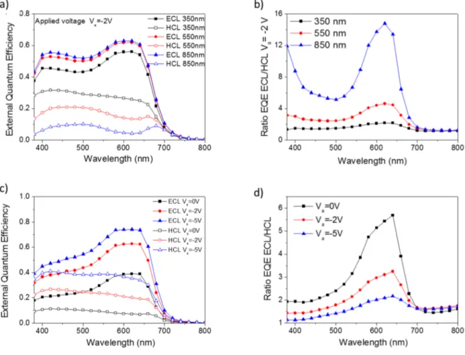
First, the external quantum efficiency (EQE) has been measured in the visible range at -2 V from the two sides (ECL and HCL) for three different active layer thicknesses: 350nm, 550nm and 850nm (Figure 2.a). The EQE ratio between the ECL and the HCL sides is plotted on Figure 2.b. It appears that the EQE is higher when the device is illuminated from the ECL side rather than from the HCL side. The EQE is measured in reverse polarization (-2 V) in order to improve the collection efficiency of the photodiode from the HCL side. In addition, the EQE dissymmetry is enhanced
when increasing the active layer thickness, and depends on the optical wavelength. The dissymmetry has been found maximum at a wavelength of 620 nm, equal to a factor of 2 (at 350 nm active layer thickness) up to 14.5 (at 850 nm active layer thickness).
Figure 2: Impact of the active layer thickness (a, b) and the applied voltage (c, d) on the difference
of quantum efficiency. In a), the EQE for the two illumination sides (HCL and ECL) measured at – 2V bias for three different active layer thicknesses: 350 nm, 550 nm and 850nm. In b), the EQE ratio between the ECL and HCL illumination side has been plotted for the three different active layer thicknesses. In c), the EQE for the two illumination sides (HCL and ECL) has been plotted at three different reverse polarizations: 0V, -2V and -5V. In d), the EQE ratio between the ECL and HCL illumination side has been plotted for three different biases. In c) and d), the active layer thickness is 550nm
Moreover, the EQE has been measured for different bias in the 550 nm active layer device: 0V, -2V and -5V, for the two illumination sides on Figure 2.c. The corresponding ratios are reported in Figure 2.d. The EQE dissymmetry is minimized when the photodiode is increasingly biased in
reverse polarization. Indeed, at 620nm, the EQE ratio is approximately equal to 6 when no polarization is applied, and drops to a factor of 2 when a negative bias of -5V is applied.
Finally, these results does not essentially change when considering the internal quantum efficiency (IQE) instead of external quantum efficiency (EQE) (as shown by simulations in supplementary material Figure S1). In fact, the internal quantum efficiency, defined as the EQE/A where A is the full device absorbance, only differs from EQE from approximately 10 %. A closer look to optical simulation results however reveals a difference of quantum efficiency when light is coming through the top or the bottom. Indeed, if we consider now the IIQE = EQE/AAL where AAL
is only the absorbance in the active layer, it can be seen from in supplementary material Figure S2 that IIQE is almost identical to IQE when light comes from the bottom, and significantly differs when light comes from the top. This is due the light absorption of the thick layer of PEDOT:PSS used in the top electrode. However, as it will be discussed later on (see section IV), the difference of light absorption is only responsible of a minor part of the EQE discrepancy, and cannot explain alone the large difference between front and back EQE, and its thickness and voltage dependency.
In conclusion, when the photodiode is biased in the reverse regime or when the active layer thickness gets thinner, the EQE dissymmetry between the two illumination sides is minimized, suggesting that the EQE ratio is reduced when the electric field inside the active layer is enhanced. Similar results has been obtained using a different fullerene molecule, the phenyl-C71-butyric acid methyl ester (PC70BM), as shown in the supplementary material Figure S3. Moreover, EQE ratios
in short circuit condition are compared between the two fullerenes as shown in the supplementary material Figure S4. The EQE ratio for the PC70BM is of the same amplitude with respect to
PC60BM, but with a different wavelength dependency, which may originates from the difference in
term of optical absorption coefficient , leading to different typical absorption length 1/. Hereinafter, this assumption is investigated.
Indeed, the optical absorption length of the active layer with the two different fullerenes has been calculated and compared with the EQE ratio in short circuit condition: with PC60BM in Figure
3.a and with PC70BM in Figure 3.b. To this aim, the optical indexes (n,k) have been extracted from
the reflection / transmission coefficients of the active layer [17]. It turns out that EQE ratio is enhanced when the absorption length is decreased, for both PC60BM and PC70BM blends. This
observation suggests that the difference of efficiency is stronger when the generation of electron /hole pairs occurs near the electrodes. More specifically, since collection through the HCL contact is less efficient than through the ECL contact, the charge collection efficiency seems weaker when pairs are generated close to the HCL.
Figure 3: Correlation between the absorption length and the front and back EQE ratio. The
calculated optical absorption length as function of wavelength is compared with the EQE ratio at 0V between the ECL and HCL illumination side. Two different fullerenes are blended with the same polymer, and a) PC60BM and b) PC70BM.
In summary, the impact of active layer thicknesses, bias and type of fullerene have been experimentally investigated. It turns out that the optical absorption length and EQE ratio are correlated, suggesting that the charge collection efficiency is degraded when electron hole pairs are generated close to the HCL electrode. This observation is in agreement with the results reported by Dibb et al [15]. Hereinafter, we attempt to identify the physical origin of this dissymmetry. As detailed later, two hypotheses have been investigated in this manuscript: diffusion of chemical species from the electrode contacts and contamination by oxygen.
III. Impact of electron and holes contact layers
The observed correlation between optical absorption length and quantum efficiency ratio has shown that the difference in term of charge collection is particularly strong when carriers are generated close to the electrodes. In addition, similar results have been obtained when the conjugated donor polymer is changed (not shown here), keeping the same device architecture. Both observations question the integrity of blend / contact interfaces. In fact, examples of degradation induced by the ECL or HCL layers can be found in the literature. For instance, in an inverted architecture, diffusion of PSS- from the PEDOT:PSS layer [18] or the photo catalyst of the polymer
induced by the ZnO in combination with light [19] have been reported. These results suggest that both contact electrodes are able to generate charges inside the active layer, such as deep traps or molecular dopants. The diffusion of chemical species from the electrodes to the active layer was also one of the assumptions invoked in [15].
400 500 600 700 1 2 3 4 5 6 R atio E Q E E C L/H C L Wavelength (nm) Ratio EQE 200 250 300 350 400 450 A bs or pt ion length ( nm ) Labs 400 500 600 700 1 2 3 4 5 6 R a tio E Q E E C L /H C L Wavelength (nm) Ratio EQE 100 150 200 250 300 Labs A b s o rp tio n le n g th (n m )
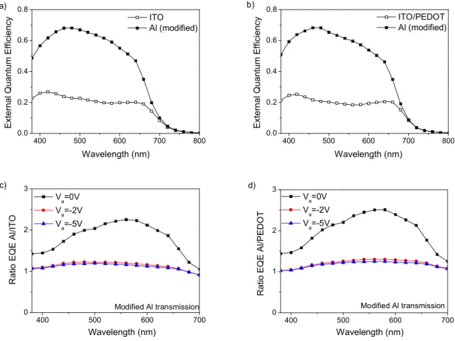
In order to investigate the role of the contact electrodes, semitransparent organic photodiodes have been processed in a direct architecture (see Fig. 1). In this case, the electron collecting electron is composed of a transparent ultra thin layer (~ 6 nm) of aluminum, i.e. a metallic electrode and not an electron collecting layer as in the previous experiments. The aluminum layer has been deposited by evaporation in a vacuum chamber. For the HCL, two types of device have been realized. In one case, only the ITO layer has been used, and in a second case, a thin PEDOT:PSS layer has been spin coated on the top of the ITO. These two devices have been introduced in order to investigate the role played by the PEDOT:PSS, which is also used in the previous samples. The active layer is 420 nm (measured by mechanical profilometer). The PC70BM
fullerene has been used in this comparison, as it enhances the EQE ratio difference.
An optical transmission spectrum of roughly 40% has been measured by UV-visible spectrometer (reported in the supplementary material Figure S5), as expected for a 6 nm thin aluminium layer. The EQE have been measured from each side. For a fair comparison, the incident light power used to calculate the EQE for the illumination through the aluminum side has been corrected to account for the excess of absorption of the aluminum layer (mentioned as “modified” on Figures 4.a and 4.b). The corresponding EQE ratios are shown in figure 4.c and 4.d, for three different polarizations: 0V, -2V and -5V. As in the case of the inverted device, the direct architecture presents a dissymmetry of efficiency between the same illumination sides. When the device is illuminated from the aluminum side (ECL side), the EQE in short circuit condition reaches an efficiency of 70% at a wavelength of 470nm whereas from the hole collecting layer an efficiency of 20 % is measured with or without PEDOT:PSS layer.
However, it has to be noticed that the EQE ratio is improved in the direct architecture devices (compared to the inverted devices): indeed, the maximum ratio is equal to 2.3 in short circuit condition at a wavelength of 580nm, whereas for the same active layer, the EQE ratio was twice more important in the case of the inverted architecture (Figure 2.b and 3.c,d). Moreover, the electric field dependency of the photocurrent has been found roughly unchanged with or without PEDOT:PSS (see in the supplementary material Figure S6), suggesting again an absence of correlation between the contact electrodes and the EQE ratio amplitude.
Figure 4: a-b) Measurement of the EQE for the two illumination sides (HCL and ECL) of direct
semi-transparent photodiode measured in short circuit condition. c-d) Corresponding EQE ratio between the ECL and HCL illumination side is calculated at three different reverse polarizations: 0V, -2V and -5V. In one case, the HCL is composed of an ITO layer only (a-c) and in the second case, the HCL also includes a PEDOT:PSS layer (b-d). The active layer is 420 nm.
Let us summarized the results obtained in this section. First of all, the difference of efficiency is still present when replacing either the electron or hole contact layers. In particular, the removal of the PEDOT:PSS does not impact the difference of EQE, which may seem surprising : indeed, as the charge collection was degraded especially when the carrier was created close to the HCL, this interface could be suspected of being a source of defects, by PSS diffusion inside the active layer for instance.
Moreover, the EQE ratio has been found improved in all devices featuring a direct architecture, compared to the inverted one. One may thus suspect the quality of the electron contact layer used in the inverted architecture. There is however another plausible explanation. Indeed, let us remind that the aluminum layer (used in the direct architecture) have been deposited by evaporation (thus in a vacuum chamber), while the electron contact layer has been deposited in air.
400 500 600 700 800 0.0 0.2 0.4 0.6 0.8 E x te rn a l Q u a n tu m E ffic ie n c y Wavelength (nm) ITO Al (modified) a) 400 500 600 700 800 0.0 0.2 0.4 0.6 0.8 b) E x te rn a l Q u a n tu m E ffic ie n c y Wavelength (nm) ITO/PEDOT Al (modified) 400 500 600 700 0 1 2 3 Modified Al transmission R a ti o E Q E A l/IT O Wavelength (nm) Va=0V Va=-2V Va=-5V c) 400 500 600 700 0 1 2 3 Modified Al transmission d) R a ti o E Q E A l/P E D O T Wavelength (nm) Va=0V Va=-2V Va=-5V
As discussed in more details later, this difference is important, and in fact explain the better results obtained using the direct architecture.
IV. Impact of oxygen contamination
Contamination by oxygen is known to be also a source of defects in polymers. In the literature [20], oxygen has been found to play a major role in the degradation of the photodiode performances, by two mechanisms: the so called “light assisted P type doping” [21, 22, 23] and polymer photo-oxidation [20].
Light assisted P-doping is usually presented as a reversible mechanism, based on the capture of free electrons (which originate from the generation of electron hole pair by light absorption), which results in the formation of a mobile hole, and a fixed negative charge, called “superoxide anions”. Oxygen molecule forms with the polymer which captured the electron, a charge transfer complex (CTC) [24, 25]. It has to be noticed that this mechanism is thermodynamically possible only when the polymer LUMO level is above the oxidation potential of the oxygen reported at 3.75eV by Nicolai et al [26].
The second mechanism caused by the presence of oxygen is the chemical degradation of the polymer itself via photo-oxidation. This degradation is irreversible, and is most likely due to the photochemical formation of carbonyl and carboxylic groups, and suspected to lead to deep trap states [20, 27, 28, 29]. In addition, these traps states are acceptor trap states, as these groups are negatively charged in the presence of electrons. The impact of oxygen on the performances of an inverted photodiode (similar to those investigated here) has been recently investigated in [31]. In this work, the front EQE of devices processed with and without oxygen plasma treatment prior to PEDOT:PSS deposition were shown to differ significantly. Using impedance spectroscopy, the authors were able to attribute this discrepancy to the presence of traps induced by oxygen.
P type doping and photo-oxidation mechanisms simultaneously occur in the presence of oxygen and light. Even if the photodiodes are encapsulated at the end of the fabrication, the potential presence of air at each process step (including the encapsulation) implies that oxygen residues may be present inside the active layer and thus could induce the two previously mentioned degradation mechanisms. In particular, P type doping as well as the formation of deep acceptor trap states caused by oxygen and light exposure could in principle both lead to the formation of a negative charged region, leading to a prejudicial electrostatic potential bending.
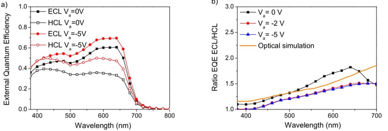
In order to investigate the impact of oxygen on front and back charge collection, devices with an inverted architecture were entirely fabricated and encapsulated in an argon filled glove box, i.e in negligible oxygen concentration atmosphere. The active layer has been processed by spin coating (and not by slot die as in previous experiments) but the target thickness has been kept at the
same nominal value 550 nm. The quantum efficiency for two different polarizations (0V and -5V) and for the two illuminations sides with their respective ratio are reported in Figure 5. Surprisingly, the photodiode performances are clearly improved with respect to photodiodes processed in air condition. In addition, the EQE ratio between the two illumination sides is strongly reduced and close to its minimum value (induced by the dissymmetry of optical transmission of the two electrodes (solid line line in Figure 5.b)). In conclusion, it appears that the absence of contaminants such as oxygen or water in the air environment where the photodiode have been processed and encapsulated, removes completely the dissymmetry of charge collection efficiency.
Figure 5: impact of the atmosphere control : a) EQE for the two illumination sides (HCL and ECL)
bias on an inverted semitransparent photodiode measured at two different reverse polarizations: 0V and -5V. The photodiode is processed and encapsulated in argon filled glove box. b) The EQE ratio between the ECL and HCL illumination side is calculated.
Figure 6: Comparison of the EQE ratio between the ECL and HCL illumination side where process
steps (P) and encapsulation (E) environments have been performed: in air or in an argon filled glove box.
To investigate more accurately the role of each process steps on the EQE ratio, a third experiment has been performed: devices have been processed in air condition, in the presence of light, but the
400 500 600 700 800 0.0 0.2 0.4 0.6 0.8 1.0 a) E x ter nal Q u antum E ffic ien c y Wavelength (nm) ECL Va=0V HCL Va=0V ECL Va=-5V HCL Va=-5V 400 500 600 700 1.0 1.5 2.0 2.5 3.0 R atio E Q E E C L/H C L Wavelength (nm) Va= 0 V Va= -2 V Va= -5 V Optical simulation b) 400 500 600 700 0 3 6 9 12 R atio E Q E E C L /H C L at 0V Wavelength (nm)
P in air, E in glove box P + E in air
encapsulation has been done in an argon filled glove box. It appears that in this latter case, the EQE dissymmetry has been reduced, but not completely removed (Figure 6). In conclusion, both the process and the encapsulation in air condition are responsible of the inclusion of air residues inside the active layer.
From these different experiments, oxygen is suspected to be the dominant factor causing charge collection dissymmetry. To confirm that the polymer used in this work can be impacted by the presence of oxygen and light via a photo-oxidation mechanism, Fourier transform infrared spectroscopy (FTIR) has been used (Figure 7). In this experiment, the active layer has been spin coated on a potassium bromide (KBr) substrate. The transmission spectrum in the infrared region is measured before and after 3 days of sunlight and air exposure. A broad absorption peak appears at 2900-3600 cm-1, which is the signature of hydroxyl (OH) group caused by the formation of
carboxyl groups. In addition, an absorption peak is observed at 1735 cm-1 which is the signature of
carbonyl groups. The apparition of these two groups, carboxyl and carbonyl groups, is the signature of the formation of covalent bond between oxygen molecules and carbon in presence of polymer [30,32]. Moreover, the absence of these two groups just after the blend deposition on the KBr substrate demonstrates that the polymer degradation mechanism occurs when the polymer is exposed to air and light. We note that the peak observed at 2300 cm-1 is related to the modification of the carbon dioxide concentration inside the analysis chamber. This experiment confirms that the polymer used in this work can be degraded by oxygen in the presence of light.
Figure 7: FTIR spectra of the polymer used in the active layer before and after 3 days in air and
exposed under an AM 1.5 light spectra.
In summary, the processing of device in a glove box has evidenced the role of air contamination in the charge collection dissymmetry inside the active layer. In addition, FTIR measurements have confirmed that the polymer was sensitive to photo-oxydation induced by
4000 3500 3000 2500 2000 1500 Carbonyl C=O T ra n s m is s io n ( a .u ) Wavenumber (cm-1) T 0 3 days exposure Hydroxyl OH C02
oxygen contamination in the presence of light. In the next section, the impact of oxygen contaminant is investigated by the mean of electrical simulations.
V. Modeling of the impact of oxygen contaminant on electrical
measurements
To further understand the role of the oxygen on the charge collection dissymmetry, electrical simulations using 1D drift diffusion, coupled with Poisson equation and 1D optical wave propagation, have been performed, following the approach proposed by Koster et al [33]. Our simulation accounts for the 1D propagation of light in the full stack, accounting for reflection, transmission, absorption and interferences. Optical indexes (n,k) have been experimentally extracted by reflection / transmission measurements on each layers [17], or taken from the literature. Layer thicknesses have been measured by mechanical profilometer.
First of all, it is clear that the difference in term of optical absorption from the front or back electrodes cannot entirely explain the large front and back quantum efficiency discrepancy. Indeed, optical transmission dissymmetry, according to simulations, is only responsible for a front/back side EQE ratio lower than 2 in the visible range (see Figure 8.b). Moreover, when considering only optical absorption, simulated EQE ratio fails to reproduce EQE dependency with wavelength and electric field. Last but not least, in absence of any traps or dopant, the theoretical value of the quantum efficiency is too large, compared to the experimental value (see Figure 8.a). This last observation confirms the electrical nature of the EQE value and front and back discrepancy.
Figure 8: a) Comparison between simulated and experimental EQE for the two illumination sides
(HCL and ECL) and their ratio (b) where no traps are included in the simulation. The inverted photodiode is processed and encapsulated in air. Symbols refer to the experimental data, solid line to simulations in absence of shallow or deep states.
As the FTIR experiments have confirmed that the polymer used in this work can be degraded by a photo-oxidation mechanism, a density of deep gap states (as proposed for instance in
400 500 600 700 0.0 0.2 0.4 0.6 0.8 1.0 simulations Ex te rn a l Q u a n tu m Ef fi c ie n c y Wavelength (nm) ECL Va=0 V HCL Va=0 V ECL Va=-5 V HCL Va=-5 V a) 400 500 600 700 1 2 3 4 5 6 R a ti o EQ E EC L /H C L Wavelength (nm) V a=0 V V a=-2 V V a=-5 V simulations b)
recombination are known to be the most effective. To simplify the model, the deep states energy distribution has been approximated by a simple single energy level. In this first simulation, no dopants or shallow traps have been implemented. Moreover, even if photo-oxidation is known to induce mostly acceptor traps, three types of deep traps have been considered at first: neutral, donor and acceptor. An acceptor trap (resp. donor) has a negative charge (resp. has no charge) when occupied by an electron, and is neutral (resp. has a positive charge) when empty. Neutral traps are supposed to remain uncharged either empty or occupied, which, of course, does not correspond to any physical situation. These unphysical defects were considered in the simulation only for the sake of comparison. Indeed, if the three type of traps induce carrier recombinations in a similar way, their impact on electrostatics differs, allowing to discriminate qualitatively the impact of recombination of carrier from the impact of active layer electrostatic charging.
It has to be noticed that the trap density has been assumed uniformly distributed in space within the active layer, assuming that oxygen has perfectly diffused inside it. This assumption is consistent with our previous analysis, which suggests that traps are more likely induced by a degradation of the full active layer, than by contacts.
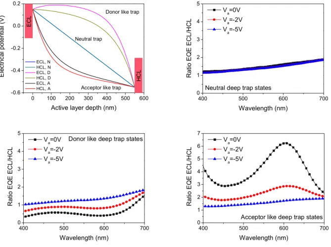
Figure 9: a) Simulated electrical potential for the three different type of gap states (neutral, donor
or acceptor) and their respective EQE ratio (b) neutral; c) donor; d) acceptor) between ECL and HCL at three different polarizations for an uniform trap concentration of 3,0 1015 cm-3.
0 100 200 300 400 500 600 -0.6 -0.4 -0.2 0.0 0.2 E C L H C L
Acceptor like trap Donor like trap
E le c tr ic al poten tial ( V )
Active layer depth (nm)
ECL, N HCL, N ECL, D HCL, D ECL, A HCL, A Neutral trap 400 500 600 700 0 1 2 3 4 5
Neutral deep trap states
R a tio E Q E E C L /H C L Wavelength (nm) Va=0V Va=-2V Va=-5V 400 500 600 700 0 1 2 3 4 5
Donor like deep trap states
R a tio E Q E E C L /H C L Wavelength (nm) Va=0V Va=-2V Va=-5V 400 500 600 700 0 1 2 3 4 5 6 7
Acceptor like deep trap states
R a tio E Q E E C L /H C L Wavelength (nm) Va=0V Va=-2V Va=-5V
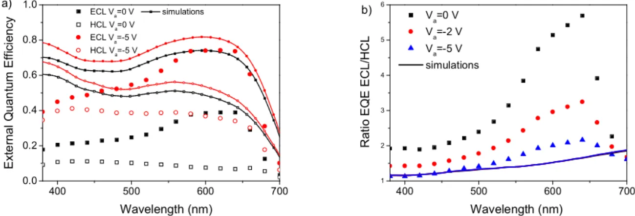
Electrical potential and EQE ratio (for different bias) have been simulated and reported in Figure 9. First of all, as expected, trap assisted recombination lead to a reduction of the quantum efficiency for all neutral, acceptor and donor traps. Moreover, the EQE ratio dependency with wavelength and electric field in the case of neutral trap states remains similar to the simulation without trap states. In addition, when charged traps are considered, a strong wavelength and electric field dependency is observed on the calculated EQE ratio. However, only the acceptor case (with a 3.01015 cm-3 concentration of acceptor deep gap states) has been found able to reproduce experimental characteristics (see Figure 10).
A closer look to simulations allows a better understanding of the physical origin of quantum efficiency dissymmetry. Indeed, while the electric field has been found uniform in the case of neutral traps within the active layer, strong electric field non uniformity appears in the simulations performed with charged traps. In the case of acceptor traps, the resulting electric field appears almost negligible close to the HCL contact. This explains why the carriers generated in the proximity of the HCL contact (and especially electrons) are more difficult to collect, and thus more impacted by recombination. This observation is consistent with the poor quantum efficiency reported when the device are illuminated by the front side. A similar phenomena occurs for donor type traps, however, the most penalized contact in this case is the ECL and not the HCL contact. It also explains why in the case of donor traps, the ECL/HCL EQE ratio is found to decrease and not to increase. This first analysis confirms that only acceptor traps can explained our experimental results, consequently, neutral and donors defects will no longer be considered in the following.
Figure 10: a) Comparison between simulated and experimental EQE for the two illumination sides
(HCL and ECL) and their ratio (b). The inverted photodiode has been processed and encapsulated in air. The active layer thickness is 550 nm. Symbols refer to experimental data, solid line to simulations, performed with a uniform concentration of 3.01015 cm-3 acceptor deep gap states.
400 500 600 700 0.0 0.2 0.4 0.6 0.8 1.0 simulation E x te rn a l Q u a n tu m E ff ic ie n c y Wavelength (nm) ECL V a=0V HCL V a=0V ECL Va=-5V HCL V a=-5V a) 400 500 600 700 0 1 2 3 4 5 6 b) R atio E Q E E C L/H C L Wavelength (nm) Va=0V Va=-2V Va=-5V Model with traps Model w/o trap
To confirm our simulation analysis, the trap assisted recombination rate and the electric field amplitude as function of the active layer depth have been plotted in Figure 11 in presence of deep acceptor traps. First of all, it turns out that the electric field is no longer uniform (as in absence of negative charges) and keeps the same spatial distribution in both front and back illumination. Moreover, the field takes significant values only at the side of the active layer close to the ECL, which implies that it is more difficult to collect charge generated close to the HCL (i.e. charge generated by the back contact). In consequence, charge generated close to the HCL are more subject to recombinations, as shown in Fig. 11.
Figure 11: Simulated electric field derived from the electrical potential (solid line), and the SRH
recombination rate (dotted line) in the active layer, when the light is sent through the electron contact layer (ECL) or through the hole contact layer (HCL). Simulations performed accounting for a uniform concentration of 3.0 1015 cm-3 acceptor deep gap states. The electron contact layer is located at x=0, while the hole contact layer is at x = 550 nm.
Figure 12: a) Comparison between simulated and experimental EQE for the two illumination sides
(HCL and ECL) and their ratio (b) at three different active layer thicknesses. The inverted photodiode has been processed and encapsulated in air. Symbols are experimental data, solid line simulations performed accounting for a uniform concentration of 3.0 1015 cm-3 acceptor deep gap
states. 0 100 200 300 400 500 0 2 4 6 8 E le c tric F ie ld E (1 0 4 V /c m ) Blend depth (nm) ECL HCL 0.0 0.4 0.8 1.2 1.6 2.0 R e c o m b in a tio n ra te R (1 0 24 /m 3 /s ) 400 500 600 700 0.0 0.2 0.4 0.6 0.8 ECL 850 nm HCL 850 nm ECL 550 nm HCL 550 nm ECL 350 nm HCL 350 nm simulation E x te rn a l Q u a n tu m E ffi c ie n c y Wavelength (nm) a) Va=-2V 400 500 600 700 0 4 8 12 16 350 nm 550 nm 850 nm simulation R a ti o E Q E E C L /H C L V a = -2 V Wavelength (nm) b)
Simulations and experiments have been compared in figure 10, 12 and 13. Device processed in air have been considered at first, in figure 9 and 11. The experimental EQE are well reproduced by simulations, not only at different polarizations (for the device with a 550 nm active layer thickness (Figure 9)), but also for different devices, featuring different active layer thicknesses (Figure 12). Remarkably, the same uniform concentration of acceptor deep trap state at 3.01015
cm-3 has been used in the two case.
Following [15], C-V experiments have also been performed (see supplementary material figure S7), allowing the estimate the doping level at 1016 cm-3, in acceptable agreement with the
value used in our simulations (3.1015 cm-3). However, only a limited part of the curve shows a linear
trend and can be used for this extraction (between 0V and -2V), as the depletion length becoming comparable to the active layer thickness, questioning the validity and accuracy of the Mott Schottky analysis in our samples.
Experimental results obtained on device processed in a filled glove box have been then compared to simulation in figure 13. Again, a very good agreement between simulations and experiments has been obtained. In this case, as expected, a lower trap concentration has been needed to fit experimental data (7.1014 cm-3). It is interesting to note that even if the trap concentration is not sufficient to induce a significant potential bending (see supplementary material figure S8) in this case (which is consistent with the experimental absence of EQE dissymmetry), however, recombinations still affect the value of quantum efficiency.
These simulations confirms that the device performances improvement observed on the sample processed in an argon filled glove box (compared to the one processed in air) can simply be explained by a difference of deep acceptor trap concentration. It further confirms the predominant role played by oxygen exposure in the degradation of performances, via the formation of deep acceptor trap states.
Figure 13: a) Comparison between simulated and experimental EQE for the two illumination sides
400 500 600 700 0.0 0.2 0.4 0.6 0.8 1.0 Simulation a) ECL Va=0V HCL Va=0V ECL Va=-5V HCL Va=-5V E x ter nal Q uantum E ffic ienc y Wavelength(nm) 400 500 600 700 1.0 1.5 2.0 2.5 3.0 b) R a tio E Q E E C L /H C L Wavelength (nm) Va= 0 V V a= -2 V V a= -5 V Simulation
filled glove box. Symbols are experimental data, solid line simulations performed accounting for a uniform concentration of 7.0 1014 cm-3 of deep acceptor trap states.
At this stage, it is clear that all experiments can be reproduced by the assumption of deep acceptor traps. However, in the literature, the impact of oxygen is sometime model as pure dopants, and not deep traps. In the following, this assumption has also been considered. To simplify, we assume doping as an efficient process, i.e. that dopant species are ionized whatever temperature and field, which of course tends to upper-estimate the impact of doping. Simulated EQE ratio at two different wavelengths (420nm and 600nm) has been plotted in Figure 14 as function of the concentration of either p type doping or deep acceptor trap states (energy level set at the middle of the gap). Results indicate that doping can indeed induce an EQE dissymmetry, such as acceptor traps. However, their impact is much less pronounced. Indeed, the EQE ratio induced by doping quickly saturates at a factor 3 for a concentration of 3.0 1015 cm-3. As in the experiments the EQE
ratio exceeds a factor 6, we conclude that the discrepancy between front and back sides illumination cannot be entirely explained by p type doping alone. An example of comparison between experiments and simulations performed with doping only is shown in the supplementary material figure S9. The different impact of doping and deep traps can be interpreted as follow. Both mechanisms induce a negative charge within the active layer, leading to potential bending (see Figure 14b) in the case of doping) and asymmetrical charge collection. However, deep acceptor traps also induce electron hole recombination, which further penalize the collection of charges.
Figure 14: a) Impact of acceptor deep traps and p type doping concentrations on front and back
EQE ratio. b) Determination of the electrical potential inside the active layer for a concentration of p type dopant of 3.0 1015 cm-3. 1 10 1 2 3 4 5 6 7 R a tio E Q E E C L /H C L a t 0 V
Doping, Trap concentration 1020/m3
P type doping 420nm 600nm Acceptor trap SRH 420nm 600nm 0 100 200 300 400 500 -0.6 -0.4 -0.2 0.0 0.2 = 420 nm = 600 nm El e c tr ic a l p o te n ti a l (V)
VI. Conclusions
In this work, the difference between the front and back quantum efficiency of organic solar cell or photodiode has been re-investigated, bringing new experimental results and new conclusions.
First of all, this effect has been quantified in a large set of samples, featuring different applied voltages, active layer thicknesses and electron and hole contact layers. Moreover, the role of oxygen has been assessed first by monitoring the difference between “air processed” and “glove box processed” device. In addition, FTIR experiments have confirmed that the polymer used in this work can be degraded by photo-oxidation induced by oxygen and light. Finally, EQE experiments have been reproduced by drift diffusion simulations, where oxygen has been taking into account as an acceptor deep trap. In particular, it has been shown that the same traps parameters can reproduce the full set of experiments, featuring different active layer thickness or applied voltage. Finally, simulations have also shown that the assumption that oxygen behaves as p type doping in the active layer cannot alone explain the large discrepancy observed in experiments.
These finding brings new elements in the understanding of the impact of oxygen contamination in the performance degradation of organic solar cell or photodiodes.
SUPPLEMENTARY MATERIAL
See supplementary material for additional information about the difference between internal quantum efficiency (IQE) vs (EQE) (Figure S1 & S2), the impact of PC70BM vs PC60BM as blend
acceptor (Figure S3 & S4), transmission spectra of the evaporated aluminum layer (Figure S5), the role of the PEDOT layer on I-V characteristic in the direct architecture (Figure S6), 1/C2 measurements performed on processed in air samples (Figure S7), potential distribution within the active layer in the low trap concentration case (Figure S8), best fit obtained in the conventional doping approximation (no traps) (Figure S9).
Acknowledgment: This work has been partially supported by the Minalogic sponsored
collaborative research project ROXTAR (FUI APP15). The authors acknowledge Simon Charlot (CEA LITEN) for his support in fabrication of OPD devices.
References:
1. Yu, G., Gao, J., Hummelen, J. C., Wudl, F., & Heeger, a. J. (1995). Science, 270(5243), 1789–1791. 2. Halls, J. J. M., Walsh, C. A., Greenham, N. C., Marseglia, E. A., Friend, R. H., Moratti, S. C., & Holmes,
A. B. (1995) Nature, 376, 498 – 500.
3. B. Norton, P.C. Eames, T.K. Mallick, M. Jun Huang, S.J. McCormack, J.D. Mondol, Y.G. Yohanis, Solar
Energy 2011, 85, 1629.
4. C.C Chen, L. Dou, R. Zhu, C.H. Chung, T.B. Song, Y.B. Zheng, S. Hawks, G. Li, P.S. Weiss, Y. Yang. ACS Nano 2012, 6, 7185.
5. Shen, L., Ruan, S., Guo, W., Meng, F., & Chen, W. Solar Energy Materials and Solar Cells, 97, 59–63. 6. J. Huang, G. Li, Y. Yang. Advanced materials 2008, 20, 415.
7. A. Kovalenko, A. Guerrero, & G. Garcia-Belmonte. ACS applied materials & interfaces, 2015 7(2), 1234-1239.
8. K.S. Chen, J.F. Salinas, H.L. Yip, L. Huo, J. Hou, A.K.Y. Jen. Energy & Environmental Science 2012, 5, 9551.
9. A. Colsmann, M. Reinhard, T.H. Kwon, C. Kayser, F. Nickel, J. Czolk, U. Lemmer N. Clarkc, J. Jasieniakc, A.B. Holmesb, D. Jonesb Solar Energy Materials and Solar Cells 2012, 98 118.
10. T. Someya, Y. Kato, S. Iba, Y. Noguchi, T. Sekitani, H. Kawaguchi, T. Sakurai. Electron Devices, IEEE
Transactions 2005, 52, 2502.
11. G.H. Gelinck, A. Kumar, J.L. van der Steen, U. Shafique, P.E. Malinowski, K. Myny, B.P. Rand, M. Simond, W. Rüttend, A. Douglasd, J. Jorritsmae, P. Heremansc, R. Andriessena, Organic
Electronics 2013, 14, 2602.
12. J. Krantz, T. Stubhan, M. Richter, S. Spallek, I. Litzov, G.J. Matt, E. Spiecker, C.J. Brabec. Advanced
Functional Materials 2013, 23, 1711.
13. Friedel, B., Keivanidis, P. E., Brenner, T. J. K., Abrusci, A., McNeill, C. R., Friend, R. H., & Greenham, N. C. Macromolecules, 2009 42(17), 6741–6747.
14. Padinger, F., Rittberger, R. S., & Sariciftci, N. S. Advanced Functional Materials, (2003), 13(1), 85–88. 15. Dibb, G. F. a., Muth, M.-A., Kirchartz, T., Engmann, S., Hoppe, H., Gobsch, G., Nelson, J. Scientific
Reports, 2013, 3, 1–7.
16. Büchele, P., Morana, M., Bagnis, D., Tedde, S. F., Hartmann, D., Fischer, R., & Schmidt, O. Organic
Electronics, 22, 29–34. (2015)
17. Smith, D. R., S. Schultz, P. Markoš, and C. M. Soukoulis. Physical Review B 65, no. 19 (2002): 195104 18. Girtan, Mihaela, and M. Rusu. Solar Energy Materials and Solar Cells 94.3 (2010): 446-450
19. Abdollahi, Y., Zakaria, A., Matori, K., Shameli, K., Jahangirian, H., Rezayi, M., & Abdollahi, T.. Chemistry Central Journal, 6(1), 100 (2012)
20. Seemann, A., Sauermann, T., Lungenschmied, C., Armbruster, O., Bauer, S., Egelhaaf, H.-J., & Hauch, J. (2011). Solar Energy, 85(6), 1238–1249.
21. Guerrero, A., Boix, P. P., Marchesi, L. F., Ripolles-Sanchis, T., Pereira, E. C., & Garcia-Belmonte, G.
Solar Energy Materials and Solar Cells (2012), 100, 185–191.
22. Liao, H.-H., Yang, C.-M., Liu, C.-C., Horng, S.-F., Meng, H.-F., Shy, J.-T., Journal of Applied Physics (2008), 103, 104506.
23. H Hintz, H Peisert, H-J Egelhaaf et T Chassé. The Journal of Physical Chemistry C (2011), vol. 115, no. 27, pages 13373, 13376.
24. Seemann, A., Egelhaaf, H.-J., Brabec, C.J., Hauch, J.A., Organic Electronics (2009)10 (8), 1424–1428. 25. Abdou, M.S.A., Orfino, F.P., Son, Y., Holdcroft, S., J. Am. Chem. Soc. (1997) 119, 4518–4525
26. Nicolai, H. T., Kuik, M., Wetzelaer, G. a H., de Boer, B., Campbell, C., Risko, C., Blom, P. W. M.
Nature Materials, (2012) 11(10), 882–7.
27. Ficker, J., Seggern, H.v., Rost, H., Fix, W., Clemens, W., McCulloch, I., Appl. Phys. Lett. (2004) 85 (8), 1377–1379.
28. A. R. Völkel, R. A. Street, and D. Knipp, Phys. Rev. B 66, 195336 (2002) 29. D. Knipp, J. E. Northrup, Adv. Mater. 21, 1–5 (2009)
30. M. Manceau, E. Bundgaard, J. E. Carlé, O. Hagemann, M. Helgesen, R. Søndergaard, M. Jørgensen et F. C Krebs. Journal of Materials Chemistry, vol. 21, no. 12, pages 4132-4141, (2011)
31. J. Euvrard, A. Revaux, A. Cantarano, S. Jacob, A. Kahn, D. Vuillaume. Organic Electronics (2018) 54 (64-71)
33. Koster, L., Smits, E., Mihailetchi, V., Blom, P. Device model for the operation of polymer/fullerene bulk heterojunction solar cells. Physical Review B, 72(8), 085205 (2005)