HAL Id: hal-01320610
https://hal.archives-ouvertes.fr/hal-01320610
Submitted on 24 May 2016HAL is a multi-disciplinary open access archive for the deposit and dissemination of sci-entific research documents, whether they are pub-lished or not. The documents may come from teaching and research institutions in France or abroad, or from public or private research centers.
L’archive ouverte pluridisciplinaire HAL, est destinée au dépôt et à la diffusion de documents scientifiques de niveau recherche, publiés ou non, émanant des établissements d’enseignement et de recherche français ou étrangers, des laboratoires publics ou privés.
Flexible White Light Emitting Diodes Based on Nitride
Nanowires and Nanophosphors
Nan Guan, Xing Dai, Agnes Messanvi, Hezhi Zhang, Jianchang Yan, E
Gautier, Catherine Bougerol, Christophe Durand, Joël Eymery, Maria
Tchernycheva
To cite this version:
Nan Guan, Xing Dai, Agnes Messanvi, Hezhi Zhang, Jianchang Yan, et al.. Flexible White Light Emitting Diodes Based on Nitride Nanowires and Nanophosphors. ACS photonics, American Chemical Society„ 2016, 3 (4), pp.597-603. �10.1021/acsphotonics.5b00696�. �hal-01320610�
Flexible white light emitting diodes based on
nitride nanowires and nanophosphors
Nan GUAN1, Xing DAI1, Agnes MESSANVI1,2,3, Hezhi ZHANG1, Jianchang YAN1,4,E. GAUTIER2,5, Catherine BOUGEROL2,6, François H. JULIEN1, Christophe DURAND2,3, Joël EYMERY2,3,*, and Maria TCHERNYCHEVA1,*.
1 Institut d’Electronique Fondamentale, UMR 8622 CNRS, Université Paris Saclay, 91405
Orsay, France
2 Université Grenoble Alpes, 38000 Grenoble, France
3 « Nanophysique et Semiconducteurs » group, CEA, INAC-SP2M, 17 rue des Martyrs,
38000 Grenoble, France
4 Institute of Semiconductors, Chinese Academy of Sciences, 100083 Beijing, China 5 CEA, INAC-SPINTEC, 17 rue des Martyrs, 38000 Grenoble, France
6 « Nanophysique et Semiconducteurs » group, CNRS, Institut Néel, 25 rue des Martyrs,
38000 Grenoble, France
*corresponding author email: maria.tchernycheva@u-psud.fr
joel.eymery@cea.fr
KEYWORDS nanowire, flexible, white LED, nitride
ABSTRACT
We report the first demonstration of a flexible white phosphor-converted light emitting diodes (LEDs) based on p-n junction core/shell nitride nanowires. GaN nanowires containing 7 radial In0.2Ga0.8N/GaN quantum wells were grown by metal-organic chemical vapor deposition
on a sapphire substrate by a catalyst-free approach. To fabricate the flexible LED, the nanowires are embedded into a phosphor-doped polymer matrix, peeled off from the growth substrate and contacted using flexible and transparent silver nanowire mesh. The electroluminescence of a flexible device presents a cool-white color with a spectral distribution covering a broad spectral range from 400 to 700 nm. Mechanical bending stress down to a curvature radius of 5 mm
White light emitting diodes (LEDs) have received worldwide attention in recent years, motivated by their significant role in reducing global energy consumption thanks to the high efficiency of solid-state lighting. Two approaches have been mainly developed. The first approach combines red, green and blue LEDs that must be carefully balanced to generate stable white light. However the dominant technology in consideration of price-performance merits relies on the second approach, which combinesa single blue nitride LED (440-460 nm) with a part of blue light down-converted with yellow phosphors (560 nm), such as for example cerium-doped yttrium aluminum garnet (YAG:Ce)1,2.
Recently, a new class of three-dimensional LEDs based on nitride nanowires (NWs) has emerged and is today intensively studied by academic laboratories and industrial groups as a potential competitor to thin film LEDs3,4. Regarding white NW LEDs, the main effort has been concentrated on the phosphor-free approach using nitride emitters with different In content to produce white light by color mixture. This approach is generally realized using axial NW LEDs grown by molecular beam epitaxy since this growth technique allows to achieve high In content required for long wavelength emission5-12. Vertical ZnO NW based LEDs with a broad visible emission band has been investigated as well13. The possibility to combine blue NW LEDs with phosphor down conversion has also been recently suggested14.
There is a strong interest to develop flexible light emitters in order to extend the LED usage to other types of applications such as for example wearable displays, curved or flexible television screens, biomedical devices and in general non-flat light sources15-18..Nowadays, the
key technology for flexible white emitters is dominated by white phosphor-converted organic LEDs (OLEDs) and white OLEDs by mixing of different colored emitters19-24. Thanks to the efforts of the past decades, OLEDs are now commercialized and offer specific advantages such as their low cost, their compatibility with various flexible substrates and a relative ease of processing. However, they still suffer from a poor time stability and from a rather low wall-plug efficiency at high luminance, especially for the blue component of the color mixture25-28. On the contrary, nitride semiconductors have excellent performance in the blue spectral range in terms of luminance and efficiency and offer a typical lifetime of 105 hours29. Therefore, there is a strong interest to develop an alternative to organic emitters by fabricating flexible white sources using nitride technology.
Flexible nitride LEDs were manufactured from 2D layers by micro-structuring and making use of a transfer process, which typically employs either laser lift-off or etching of a sacrificial layer17,30-33. Alternatively, nanostructures such as NWs or micro-pyramids have been used to fabricate blue and green flexible LEDs34-38.In addition to nitrides, ZnO NW arrays grown directly on a flexible substrate have been used to demonstrate LEDs with a broad visible emission band39-41.One additional interest in downscaling the emitter size is the possibility to achieve quasi-continuous extended emitters with a small volume of the active material without the need for light-spreading plates used in display backlighting systems based on standard nitride LEDs42. Recently, we have demonstrated flexible bi-color LEDs based on vertical nitride NWs encapsulated into a flexible polymer membrane38. However, no flexible white phosphor-converted NW LED has ever been reported so far.
Here we demonstrate and characterize flexible phosphor-converted white LEDs based on core/shell n-p junction NWs grown by catalyst-free metal-organic chemical vapor deposition (MOCVD). The active region contains 7 radial InGaN/GaN quantum wells producing a blue electroluminescence peaked at ~437 nm. To form the flexible devices, the NWs are embedded into polydimethylsiloxane (PDMS) mixed with YAG:Ce nanophosphors, peeled-off from their growth substrate and contacted using a silver nanowire transparent mesh. Large area (~5×6mm2) flexible devices are fabricated. The flexible LEDs exhibit a cool-white electroluminescence (EL) with a broad wavelength spectrum from 400 to 700 nm covering almost the entire visible range. The device bending down to radii of 5 mm does not show any performance degradation. The maximal measured external quantum efficiency (EQE) of the white flexible LED is 9.3% and the wall plug efficiency is 2.4%. This technology opens prospects for future efficient, high-brightness and large area flexible white light sources.
EXPERIMENTAL METHODS
Self-assembled GaN NWs with core/shell n-p junction based on radial InGaN/GaN multiple quantum wells (MQWs) were used for device fabrication as a blue light source. These wires were grown on c-sapphire substrates by MOCVD in a closed coupled showerhead reactor. The method to grow catalyst-free 𝑐 -axis GaN NWs consists of the following steps: (i)in situ pretreatment of the sapphire surface (bake and ammonia nitridation) to promote the formation of a N-polar surface, (ii)in situ thin SiNx layer deposition acting as a partial mask, (iii) nucleation of
GaN seeds, and then (iv) growth of GaN NWs at 1040°C and 800 mbar combining a low V/III ratio (with trimethylgallium (TMGa) and ammonia (NH3) as III and V precursor, respectively)
and a high silane (SiH4) flux to favor the vertical growth (see details in ref. 43). A highly
n-doped GaN segment (~10 µm, 1020 cm-3) was grown first, followed by a nointentionally n-doped GaN segment (~15 µm, 1019 cm-3). Then, 7 InGaN/GaN quantum wells were radially grown around the GaN NWs at 400 mbar using triethylgallium (TEGa), trimethylindium (TMIn), and ammonia (NH3)44,45. The InGaN wells (resp. GaN barriers) were grown at 720°C (resp.
900°C) with a targeted thickness of 3 nm (resp. 10 nm) and an In content of about 20%. The quantum wells were covered with a p-doped thick GaN shell grown at 920°C using biscyclopentadienyl-magnesium precursor (Cp2Mg) followed by an activation dopant annealing
(20 min, 750°C under N2) leading to a few 1017 cm-3hole concentration. Note that the quantum
wells and the p-GaN shell do not grow on the highly n-doped base part of the GaN NWs due to the spontaneous formation of a SiNx passivation layer on the wire sidewalls related to silane
injection46. Fig. 1a) and b) show scanning electron microscopy (SEM) images of as-grown NWs with a typical wire density of about 106 cm-2 and a diameter in the core/shell part varying from 700 nm to 2 µm. The internal NW structure is illustrated in the schematic of Figure 1b). The radial growth of the MQWs and p-GaN is evidenced in Fig. 1c) showing a transversal cross-section image obtained by scanning transmission electron microscopy (STEM) using high-angle annular dark-field (HAADF) detector. The wire slice is prepared by focus ion beam technique with an orientation perpendicular to the wire growth c-axis. The STEM image taken along the [0001] zone axis allows to estimate the typical thickness of wells and barriers to be 3.5 and 14 nm, respectively. The thickness of the p-GaN shell is about 160 nm. Structural defects (mainly dislocation and stacking faults) are visible on the shell part (white lines) as previously reported in Ref. 47.
Figure 1. a) 30° tilted SEM image of core/shell InGaN/GaN NW grown on c-sapphire. b) Detail of a single wire showing the core/shell QW region and its schematics. c) Transversal cross-sectional STEM-HAADF image taken along the c-zone axis showing the shell structure with the MQWs and p-GaN.
A commercial nanophosphor YAG:Ce (3.3 %wt) has been selected for demonstration purpose (see the SEM image in the inset of Fig. 2)). It absorbs the blue LED radiation through the allowed 4f1→5d1 Ce3+ transition and emits yellow light via the reverse mechanism. These nanophosphors represent a benchmark for LED phosphors with a strong absorption for blue LED, a fast decay time that prevents saturation quenching and no time degradation due to the environment or optical excitation. The quantum efficiency of such materials is generally larger than 85 %, but many optimizations using other ions (Eu2+, Mn4+…) and ceramics (oxides, halides…) are still under way to maximize the conversion efficiency and the color rendering48. The inset of Fig. 2 shows the SEM image of the nanophosphors with a grain size smaller than 500 nm, which is completely compatible with the space around the wire assembly of Fig. 1a). The emission and excitation of the selected nanophosphor has been measured by a Hitachi F-4500 spectrophotometer in PDMS, water and acetonitrile to check their dependency on the environment (via the dielectric effect and different agglomeration due to the matrix ionicity and mixing conditions). The typical emission (ex502 nm) and excitation (em568 nm) spectra of
nanophosphors in PDMS are shown in Fig. 2 (mass ratio YAG:Ce phosphor/PDMS=1:20). The excitation spectrum reveals two broad bands at about 350 and 500 nm wavelengths, respectively, arising from the 4f (4f1) to 5d (4f0 5d1) transitions in the electronic configuration of Ce3+. The 500 nm peak has two components at about 450 and 500 nm coming from the interaction of the phosphors with PDMS or agglomeration (see the discussion in supplementary materials with the measurements in water and acetonitrile). These bands, as discussed later, match with the blue emission of commercial (In)GaN chips and also match the electroluminescence of the core/shell NW LED used for phosphor pumping in this investigation. The emission spectrum has a similar large full width at half maximum (FWHM) of 0.4 eV with a maximum centered at 568 nm wavelength compatible with the realization of a white light emitter.
Figure 2. Emission (ex502 nm) and excitation (em568 nm) spectra of Y3Al5O12:Ce3+
(3.3 % wt.) nanophosphors embedded in PDMS. The inset shows an SEM image of the nanophosphors.
Fig. 3 illustrates the fabrication steps of the flexible white LEDs. First, a Ni/Au (3nm/3nm) layer is sputtered on the InGaN/GaN shell after protection of the lower n+-GaN part by a photo-resist. After the lift-off of the photo-resist, the Ni/Au layer is annealed at 400 °C under oxygen. This step is crucial to achieve an ohmic top contact with the silver nanowire transparent mesh. PDMS doped with YAG:Ce phosphor (mass ratio YAG:Ce phosphor : PDMS=1:20) is then spin-coated on the NW array to fill the space between the NWs. It should be noted that the phosphor powder has been milled before being mixed into PDMS to reduce the agglomeration of phosphors. Nevertheless some phosphor lumps with a diameter ~10 µm could be found in PDMS. The PDMS/NW composite film (~25-30µm) is peeled off and the shell side of NWs is attached to an arbitrary host substrate. Then a Ti/Al/Ti/Au metallization is applied to the n+-GaN side. The NW/PDMS membrane is again removed from the substrate and attached to a metal foil, which plays the role of an external flexible contact connecting the n+-GaN side. The PDMS residues are etched to uncover the NW top parts. Silver NWs are then spin-coated to form the top transparent flexible electrode connecting the p-GaN side of the NWs. Finally, the LED surface is capped with PDMS mixed with YAG:Ce phosphor to enhance the light conversion. The surface of the fabricated white LED is 5×6 mm2.
A reference flexible blue LED sample has been fabricated for comparison using another piece of the same InGaN/GaN NW wafer and following the same procedure as described above but without the phosphor addition. The EL spectrum of the reference blue LED under 9 V bias is shown in Fig. 5. The blue peak at 437 nm wavelength is ascribed to the emission of the core-shell QWs and the green peak at ~479 nm wavelengthoriginates from the axial QW emission, as previously discussed in Ref. 49.
Figure 3. Fabrication process flow of the flexible white LEDs based on free-standing polymer-embedded NWs.
RESULTS AND DISCUSSION
The electrical properties of the flexible LEDs were characterized in a probe station using a Keithley 2636 source meter. The current density-voltage (J-V) curve of the flexible white LED is shown in Figure 4. Two scales are presented showing the current per NW (estimated from the density of contacted NWs according to statistics performed on the SEM images) and the current density in the active radial quantum wells. In order to estimate the current density in the active region, we have assumed as a first approximation that the total surface of the p-GaN shell region of all contacted NWs contributes to the current. This assumption is likely to result in an underestimation of the actual current density. Indeed, because of the resistivity of the p-doped GaN shell the current is expected to be mainly concentrated in the upper part of the core/shell region, which is contacted by the silver NWs. Assuming no current spreading in the p-doped GaN shell, the current density values in Fig. 4 would be increased by a factor of 5. As seen in Fig. 4, the J-V characteristics show a rectifying diode-like behavior with an opening voltage around 3 V. The reverse leakage current remains below 0.6 A/cm2 for biases up to -7 V. The EL can be detected at positive biases larger or equal to 3.5 V. For comparison, the J-V characteristics of the reference blue LED are shown in Figure. S3.
Figure 4. J-V characteristicsof the flexible white LED. The inset shows the same J-V curve in logarithmic scale.
The EL of the white LED and of the reference blue LED has been measured at room temperature. Figure 5 shows the EL spectra together with the PL of the nanophosphors embedded in PDMS. The EL spectrum of the white LED presents a broad wavelength distribution from 400 nm to 700 nm covering almost the entire visible spectrum range. The dominant emission in the EL spectrum coming from the phosphorous luminescence is peaked at 489 nm and spreads up to 700 nm. A shoulder corresponding to the remaining unconverted blue EL of the NWs peaked at 437 nm is also observed.
Figure 5. EL spectra under 9 V bias of the blue NW LED (blue curve) and of the flexible white LED (green curve), PL spectrum of the nanophosphors embedded into PDMS excited at 502 nm wavelength (red curve).
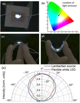
The operation of the flexible LED has been tested under different bending conditions. Fig. 6 shows photographs of the emitting flexible white LED in a flat configuration (panel a) and with bending radii of 5 mm (panel c) and -5 mm (panel d). The emission color appears as cool-white. No significant change of either the current or the EL spectrum has been observed upon bending. After 10 bending cycles, no appreciable change appeared in the J-V or EL characteristics compared to the original LED performance. No degradation of the current and the EL emission was observed after 50 days storage of the LED in ambient conditions without any external encapsulation.
We have estimated the XYZ tristimulus values of the Commission International de l’Eclairage (CIE) 1931. The XYZ color space values were calculated from the EL spectrum by the CIE color-matching functions. The chromaticity coordinates x and y were obtained as follows: 𝑥 =𝑋+𝑌+𝑍𝑋 and 𝑦 =𝑋+𝑌+𝑍𝑌 . The device emission characteristics are illustrated in the CIE 1931 chromaticity diagram shown in Fig. 6b) under an injection current of 3.9 A/cm2, corresponding to a bias of 5 V. The LED color locates at x = 0.3011, y=0.4688 outshining cool-white light with a correlated color temperature (CCT) of 6306 K and with a color rendering index (CRI) of 54.
Figure 6. Photographs of the operating flexible white LED under bending radii of (a) infinity (c) 5 mm (d) -5 mm. (b) CIE 1931 chromaticity diagram of flexible white LEDs under injection current density of 3.9 A/cm2 (chromaticity coordinates x=0.3011, y=0.4688; CCT= 6306 K; CRI=54). (e) Intensity distribution diagram of the flexible white LED (red)and that of a reference ideal Lambertian source (blue) as a function of the emission angle.
The dependence of the electroluminescence (EL) intensity on the injection current has been investigated. Fig. 7 displays the EL spectra for increasing biases ranging from 4 V to 9 V. The spectral distribution covers a broad spectral range from 400 to 700 nm with a peak at around 490 nm. The blue NW EL is visible in the spectra as a shoulder at 437 nm. No significant shift of the peak wavelength can be observed when increasing the injection current.
The emitted power of the flexible white LEDwas estimated using a power-meter with a calibrated flat spectral response. Fig. 6 e) shows the measured intensity distribution diagram as a function of the emission angle. At 50% of the peak intensity, the light is confined in a 45° angle. The measured intensity distribution diagram of the reference blue LED is shown in Figure S5. Both of the white and blue LEDs have a Lambertian source like behavior.The white LED was then positioned at a distance of 1.1 cm from the power-meter with a sensor diameter of 1.6 cm. As a result, only the emission with a light cone angle of 72° is detected. The LED emission under the maximal applied bias of 11 V (current density 20.84 A/cm2) measured by the power-meter sensor is 7.5 mW.
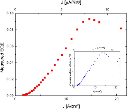
Fig. 8 shows the external quantum efficiency (EQE) and wall-plug efficiency (WPE) as a function of the injection current density based on the measured emission power. The EQE is defined as EQE =𝑛𝑝 ℎ 𝑜𝑡𝑜𝑛
𝑛𝑒− , where 𝑛𝑝ℎ𝑜𝑡𝑜𝑛is the number of photons emitted from the white LED
and 𝑛𝑒−is the number of electrons passing through the device. From the EL spectrum of the
white LED, 𝑛𝑝ℎ𝑜𝑡𝑜𝑛is calculated by the following formula: 𝑛𝑝ℎ𝑜𝑡𝑜𝑛 = 𝐼(𝜆) ℎ𝑐 𝜆
𝑑𝜆 where 𝐼(𝜆) is the measured optical intensity distribution normalized to get the integrated power equal to the experimental value𝑃𝑜𝑝𝑡𝑖𝑐 and ℎ𝑐𝜆 is the photon energy at wavelength λ. The WPE is defined as
WPE = 𝑃𝑜𝑝𝑡𝑖𝑐
𝑃𝑒𝑙𝑒𝑐𝑡𝑟𝑖𝑐 , where 𝑃𝑜𝑝𝑡𝑖𝑐 is the optical power of the white LED measured by the
power-meter and 𝑃𝑒𝑙𝑒𝑐𝑡𝑟𝑖𝑐 is the injected electrical power.
At maximum the value of the EQE is 9.3% and that of the WPE is 2.4% under an injection current density of 14.6 A/cm2. It should be noted that these value are underestimated because of the underestimation of the actual emission power of the LEDs. Accounting for the limited solid angle used in the power measurements and for the intensity distribution diagram shown in Fig. 6e), the actual values of the emission power, EQE and WPE should be multiplied by a factor of 1.42, i. e. 10.7 mW, 13.2% and 3.4% for the power, EQE and WPE, respectively. The EQE exhibits a droop starting from 14.6A/cm2 current density under the assumption that the total surface of the p-GaN shell region of all contacted NWs contributes to the current. (If no current spreading in the p-doped GaN shell is assumed, the droop appears at higher current density values of 73 A/cm2.)The WPE and EQE characteristics of the reference blue LED are shown in Figure. S4.
Figure 8. Room temperature EQE deduced from the measured optical power versus the injection current density (lower scale) and the current per NW (upper scale). The inset shows the WPE.
The absolute quantum efficiency versus the wavelength of the YAG:Ce phosphors is reported in Figure S2. The maximal yield of ~60% is achieved at a wavelength of 440 nm. This measured absolute quantum efficiency is consistent with an estimation from the wall-plug efficiency of the blue and white LEDs. Indeed, the conversion efficiency of the nanophosphor can be estimated as the following definition:
η𝑝ℎ𝑜𝑠𝑝ℎ𝑜𝑟 = 𝑊𝑃𝐸𝑤 ℎ 𝑖𝑡𝑒
𝑊𝑃𝐸𝑏𝑙𝑢𝑒 where 𝑊𝑃𝐸𝑏𝑙𝑢𝑒 and 𝑊𝑃𝐸𝑤ℎ𝑖𝑡𝑒 are the WPE values of the blue NW
LED and of the white LED, respectively. Using their maximal values (𝑊𝑃𝐸𝑏𝑙𝑢𝑒 = 4.2%𝑊𝑃𝐸𝑤ℎ𝑖𝑡𝑒 = 2.4% ), the estimated nanophosphor conversion efficiency is
η𝑝ℎ𝑜𝑠𝑝 ℎ𝑜𝑟 = 57.1%.
CONCLUSION
In summary, flexible white phosphor-converted LEDs based on p-n junction core/shell nitride nanowires have been demonstrated. Blue light from the inorganic semiconductor NW LEDs is down-converted with a yellow phosphor mixed in a flexible transparent polymer matrix embedding the NWs to generate a cool-white light. Metal foil and Ag-nanowires provide respectively the down and top electrical contacts ensuring high conductivity and mechanical flexibility. No degradation of the current and the EL emission was observed during bending or after 50 days storage in ambient conditions without any external encapsulation. This technology opens interesting possibilities for future high efficient flexible white lighting applications as well as for curved and flexible displays.
Acknowledgements
This work has been financially supported by ANR-14-CE26-0020-01 project “PLATOFIL”, EU H2020 ERC project “NanoHarvest” (grant no. 639052) and French national Labex GaNex (ANR-11-LABX-2014). The device fabrication was realized at CTU-IEF-Minerve technological platform, member of the Renatech RTB network. The authors thank also J.
Dussaud for technical MOCVD support. We also thank G. Le Blevennec and O. Renard for phosphor supply as well as P. Chenevier for spectrophotometry measurements.
References
[1] Nakamura, S. Present performance of InGaN based blue/green/yellow LEDs, Proc. SPIE 3002, 1997, 26–35.
[2] Pimputkar, S.; Speck, J. S.;DenBaars, S. P.;Nakamura,S. Prospects for LED lighting, nature photonics, 2009, 3, 180.
[3] Li, S.; Waag, A. GaN based nanorods for solid state lighting, J. Appl. Phys.,2012, 111, 071101.
[4] Kang, M.; Lee, C.; Park, J. B.; Yoo, H.; Yi, G. Gallium nitride nanostructures for light-emitting diode applications, Nano Energy, 2012, 1, 391.
[5] Armitage, R.; Tsubaki, K. Multicolour luminescence from InGaN quantum wells grown over GaN nanowire arrays by molecular-beam epitaxy, Nanotechnology, 2010, 21, 195202.
[6] Guo, W.; Banerjee, A.;Bhattacharya, P.;Ooi, B. S.; InGaN/GaN disk-In-nanowire white light emitting diodes on (001) silicon, Appl. Phys. Lett., 2011, 98, 193102.
[7] Guo, W.; Zhang,M.;Banerjee,A.; Bhattacharya, P. Catalyst-Free InGaN/GaN Nanowire Light Emitting Diodes Grown on (001) Silicon by Molecular Beam Epitaxy, Nano Lett., 2010, 9, 3355–3359.
[8] Lin, H.; Lu ,Y.; Chen, H.; Lee,H.; Gwo, S.InGaN/GaN nanorod array white light-emitting diode, Appl. Phys. Lett., 2010, 97, 073101.
[9] Sadaf, S. M.; Ra, Y.H.;Nguyen, H. P. T.; Djavid,M.; Mi,Z. Alternating-Current InGaN/GaN Tunnel Junction Nanowire White-Light Emitting Diodes, Nano Lett., 2015, 10,6696–6701.
[10] Nguyen, H. P.,Djavid, M. S.; Woo, Y.; Liu,X.; Connie, A.T.; Sadaf, S. ;Wang, Q.; Botton, G.A.;Mi, I. Z. Engineering the carrier dynamics of InGaN nanowire white light-emitting diodes by distributed p-AlGaN electron blocking layers,Scientific Reports,2015, 5, 7744.
[11] Nguyen, H. P.;Zhang, S.;Ashfiqua, T. C.;Kibria, M. G.; Wang, Q.; Shih, I.; Mi, Z. Breaking the Carrier Injection Bottleneck of Phosphor-Free Nanowire White Light-Emitting Diodes,Nano Lett., 2013,11, 5437–5442.
[12] Nguyen, H. P.; Wang, Q.; Mi, Z.Phosphor-Free InGaN/GaN Dot-in-a-Wire White Light-Emitting Diodes on Copper Substrates, Journal of Electronic Materials,2014, 43, 868-872.
[14] Schimpke, T.; Mandl, M.; Stoll, I.; Pohl-Klein, B.; Bichler, D.; Zwaschka, F.; Strube-Knyrim, J.; Huckenbeck, B.; Max, B.; Müller, M.; Veit, P.; Bertram, F.; Christen, J.; Hartmann, J.; Waag, A.; Lugauer, H.;Strassburg, M. Phosphor-converted white light from blue-emitting InGaN microrod LEDs, Phys. Status Solidi A, 2016, 1–8, DOI 10.1002/pssa.201532904
[15] Lee, S. Y.;Park, K. I.;Huh, C.;Koo, M.;Yoo, H. G.;Kim, S.;Ah, C. S.;Sung, G. Y.;Lee, K. J. Water-resistant flexible GaN LED on a liquid crystal polymer substrate for implantable biomedical applications, Nano Energy, 2012, 1,145–151.
[16] Kim,R. H.;Kim, D. H.;Xiao, J.;Kim, B. H.;Park, S. I.;Panilaitis, B.;Ghaffari, R.;Yao, J.;Li, M.;Liu, Z.;Malyarchuk, V.; Kim, D. G.;Le, A. P.;Nuzzo, R. G.;Kaplan, D. L.;Omenetto, F. G.;Huang, Y.;Kang, Z.;Rogers, J. A. Waterproof AlInGaP optoelectronics on stretchable substrates with applications in biomedicine and robotics, Nat. Mater., 2010, 9, 929–937.
[17] Goßler, C.;Bierbraue, C.;Moser, R.;Kunzer, M.; Holc, K.;Pletschen, W.; Kohler, K.;Wagner, J.;Schwaerzle, M.;Ruther, P.;Paul, O.;Neef, J.;Keppeler, D.;Hoch, G.;Moser, T.;Schwarz, U. T. GaN-based micro-LED arrays on flexible substrates for optical cochlear implants, J. Phys. D: Appl. Phys., 2014, 47, 205401.
[18] Sher, C.;Chen, K.;Lin, C.;Han, H.;Lin, H.;Tu, Z.;Tu, H.;Honjo, K.;Jiang, H.;Ou, S.;Horng, R.;Li, X.;Fu, C.;Kuo, H. Large-area, uniform white light LED source on a flexible substrate, Optics Express, 2015, 23, A1167-A1178.
[19] Reineke, S.;Thomschke, M.;Lüssem, B.;Leo, K.; White organic light-emitting diodes: Status and perspective, Rev. Mod. Phys., 2013, 85, 1245.
[20] Baldo, M. A.; O'Brien, D. F.; You, Y.; Shoustikov, A.; Sibley, S.; Thompson, M. E.; Forrest, S. R. Highly Efficient Phosphorescent Emission from Organic, Nature, 1998, 395, 151-154.
[21] Sebastian, R.;Frank, L.;Gregor, S.;Nico, S.;Karsten, W.;Björn, L.; Karl, L. White organic light-emitting diodes with fluorescent tube efficiency, Nature, 2009, 459, 234-238.
[22] Kido, J.; Kimura, M.; Nagai, K.; Multilayer White Light-Emitting Organic Electroluminescent Device, Science, 1995, 267, 1332–1334.
[23] Reineke, S.;Lindner, F.;Schwartz, G.;Seidler, N.;Walzer, K.;Lussem, B.;Leo,K. White organic light-emitting diodes with fluorescent tube efficiency, Nature,2009, 459, 234.
[24] Rosenow, T. C.;Furno, M.;Reineke, S.;Olthof, S.;Lussem, B.;Leo, K. Highly efficient white organic light-emitting diodes based on fluorescent blue emitters, J. Appl. Phys. 2010, 108, 113113.
[25] Adamovich, V. High-performance phosphorescent white-stacked organic light-emitting devices for solid-state lighting, Journal of Photonics for Energy, 2012, 2, 021202.
[26] So, F.; Kondakov, D. Degradation Mechanisms in Small-Molecule and Polymer Organic Light-Emitting Diodes, Advanced Materials, 2010, 22, 3762–3777.
[27] Thejokalyani, N.; Dhoble, S. J. Organic Light-Emitting Materials and Devices, Renewable Sustainable Energy Rev.,2014, 32, 448−467.
[28] Lee, C. W.;Lee, J. Y. Above 30% external quantum efficiency in blue phosphorescent organic light-emitting diodes using pyrido[2,3-b]indole derivatives as host materials, Adv Mater., 2013, 25, 5450.
[29] Jiang, H. X.;Lin, J. Y. Nitride micro-LEDs and beyond -a decade progress review, Opt. Express, 2013, 21, A475−84.
[30] Chun, J.;Hwang, Y.;Choi, Y.;Jeong, T.;Baek, J. H.;Ko, H. C.;Park, S.; Transfer of GaN LEDs from sapphire to flexible substrates by laser lift-off and contact printing, IEEE Photonics Technology Letters, 2012, 24, 2115-2118.
[31] Sher, C.;Chen, K.;Lin, C.;Han, H.;Lin, H.;Tu, Z.;Tu, H.;Honjo, K.;Jiang, H.;Ou, S.;Horng, R.;Li, X.;Fu, C.;Kuo, H.; Large-area, uniform white light LED source on a flexible substrate, Opt Express,2015; 23, A1167-78.
[32] Lee, S. Y.;Park, K.;Huh, C.;Koo, M.;Yoo, H. G.;Kim, S.;Ah, C. S.;Sung, G. Y.;Lee, K. J.Water-resistant flexible GaN LED on a liquid crystal polymer substrate for implantable biomedical applications, Nano Energy, 2012, 1, 145.
[33] Choi, W.; Park, H. J.; Park, S.; Jeong, T. Flexible InGaN LEDs on a polyimide substrate fabricated using a simple direct-transfer method, IEEE PTL, 2014, 26, 2115.
[34] Choi, J. H.; Cho, E. H.; Lee, Y. S.;Shim, M.; Ahn, H. Y.; Baik, C.; Lee, E. H.;Kim, K.; Kim, T.; Kim, S.; Cho, K.; Yoon, J.;Kim, M.; Hwang, S.Fully Flexible GaN Light-Emitting Diodes through Nanovoid-Mediated Transfer, Adv. Opt. Mater., 2014, 2, 267.
[35] Wang, L.;Ma, J.;Liu, Z.;Yi, X.;Zhu, H.;Wang, G. In Situ Fabrication of Bendable Microscale Hexagonal Pyramids Array Vertical Light Emitting Diodes with Graphene as Stretchable Electrical Interconnects, ACS Photonics,2014, 1, 421−429.
[36] Chung, K.; Beak, H.; Tchoe, Y.; Oh, H.; Yoo, H.; Kim M.; Yi, G.;Growth and characterizations of GaN micro-rods on graphene films for flexible light emitting diodes, APL Mater., 2014, 2, 092512.
[37] Lee, C.; Kim, Y.; Hong, Y. J.; Jeon, S.; Bae, S.; Hong, B. H.; Yi, G. Flexible Inorganic Nanostructure Light-Emitting Diodes Fabricated on Graphene Films, Advanced Materials,2011, 23, 4614.
[38] Dai, X.;Messanvi, A.;Zhang, H.;Durand, C.;Eymery, J.;Bougerol, C.;Julien, F. H.;Tchernycheva,M. Nano Letters, 2015, 10, 6958–6964.
[39] Bano, N., Zaman, S., Zainelabdin, A., Hussain, S., Hussain, I., Nur, O. and Willander, M., 2010. ZnO-organic hybrid white light emitting diodes grown on flexible plastic using low temperature aqueous chemical method. Journal of Applied Physics, 108(4), p.043103.
[40] Sun, X.W., Huang, J.Z., Wang, J.X. and Xu, Z., 2008. A ZnO nanorod inorganic/organic heterostructure light-emitting diode emitting at 342 nm. Nano Letters, 8(4), pp.1219-1223.
[41] Nadarajah, A., Word, R.C., Meiss, J. and Könenkamp, R., 2008. Flexible inorganic nanowire light-emitting diode. Nano letters, 8(2), pp.534-537.
[42] Morkoç, H. GaN-based Optical and Electronic devices, Wiley, Handbook of Nitride Semiconductors and Devices, 2009, 3.
[43] Koester, R.;Hwang, J.S.;Durand, C.;Dang, D.L.S.; Eymery, J. Self-assembled growth of catalyst-free GaN wires by metal–organic vapour phase epitaxy, Nanotechnology, 2010, 21, 015602
[44] Koester, R.;Hwang, J.;Salomon, D.;Chen, X.;Bougerol, C.;Barnes, J.;Le, D.;Dang, S.;Rigutti, L.;Bugallo, A.D.L.;Jacopin, G.;Tchernycheva, M.;Durand, C.;Eymery, J.;M-Plane Core–Shell InGaN/GaN Multiple-Quantum-Wells on GaN Wires for Electroluminescent Devices, Nano Lett., 2011, 11, 4839.
[45] Chen, X. J.;Perillat-Merceroz, G.;Sam-Giao, D.;Durand, C.; Eymery, J. Homoepitaxial growth of catalyst-free GaN wires on N-polar substrates, Appl. Phys. Lett., 2010, 97, 151909.
[46] Eymery, J.;Salomon, D.;Chen, X.;Durand, C. Process for Catalyst-Free Selective Growth on a Semiconductor Structure, 2012, Patent WO2012136665.
[47] Koester, R.; Hwang, J.; Salomon, D.; Chen, X.; Bougerol, Catherine.; Barnes, J.; Dang, D. L. S.; Rigutti, L.; Bugallo, A. de L.; Jacopin, G.; Tchernycheva, M.; Durand, C.; Eymery, Joël. M-Plane Core–Shell InGaN/GaN Multiple-Quantum-Wells on GaN Wires for Electroluminescent Devices, Nano Lett., 2011, 11, 4839–4845.
[48] Setlur, A. A. Phosphors for the LED-based Solid State Lighting, The Electrochemical Society Interface,2009, 16, 32.
[49] Jacopin, G.;Bugallo, A. de L.;Lavenus, P.;Rigutti, L.;Julien, F. H.;Zagonel, L. F.;Kociak, M.;Durand, C.;Salomon, D.;Chen, X. J.;Eymery, J.;Tchernycheva M. Single-Wire Light-Emitting Diodes Based on GaN Wires Containing Both Polar and Nonpolar InGaN/GaN Quantum Wells , Applied Physics Express, 2012, 5, 014101.
FOR TABLE OF CONTENTS USE ONLY
Flexible white light emitting diodes based on nitride nanowires and nanophosphors Nan GUAN1, Xing DAI1, Agnes MESSANVI1,2,3, Hezhi ZHANG1, Jianchang YAN1,4,E. GAUTIER2,5, Catherine BOUGEROL2,6, François H. JULIEN1, Christophe DURAND2,3, Joël EYMERY2,3,*, and Maria TCHERNYCHEVA1,*.
1 Institut d’Electronique Fondamentale, UMR 8622 CNRS, Université Paris Saclay, 91405 Orsay, France
2 Université Grenoble Alpes, 38000 Grenoble, France
3 « Nanophysique et Semiconducteurs » group, CEA, INAC-SP2M, 17 rue des Martyrs,
38000 Grenoble, France
4 Institute of Semiconductors, Chinese Academy of Sciences, 100083 Beijing, China 5 CEA, INAC-SPINTEC, 17 rue des Martyrs, 38000 Grenoble, France
6 « Nanophysique et Semiconducteurs » group, CNRS, Institut Néel, 25 rue des Martyrs,
38000 Grenoble, France
*corresponding author email: maria.tchernycheva@u-psud.fr
joel.eymery@cea.fr
KEYWORDS nanowire, flexible, white LED, nitride
Schematic diagram (left) and photo (right) of the bended flexible white LED ABSTRACT
We report the first demonstration of a flexible white phosphor-converted light emitting diodes (LEDs) based on p-n junction core/shell nitride nanowires. GaN nanowires containing 7 radial In0.2Ga0.8N/GaN quantum wells were grown by metal-organic chemical vapor deposition
on a sapphire substrate by a catalyst-free approach. To fabricate the flexible LED, the nanowires are embedded into a phosphor-doped polymer matrix, peeled off from the growth substrate and contacted using flexible and transparent silver nanowire mesh. The electroluminescence of a flexible device presents a cool-white color with a spectral distribution covering a broad spectral