S1
A Close Look at Charge Generation in Polymer:Fullerene Blends with
Microstructure Control
Mariateresa Scarongella,
aJelissa De Jonghe-Risse,
aEster Buchaca-Domingo,
bMartina Causa’,
cZhuping Fei,
dMartin Heeney,
dJacques-E. Moser,
aNatalie Stingelin,
band Natalie Banerji*
a,cSupporting Information
a
Institute of Chemical Sciences & Engineering, Ecole Polytechnique Fédérale de Lausanne (EPFL), SB ISIC GR-MO, Station 6, CH-1015 Lausanne, Switzerland.
b Centre for Plastic Electronics and Department of Materials, Imperial College London, Exhibition Road,
Lon-don, SW7 2AZ, United Kingdom.
cDepartment of Chemistry, University of Fribourg, Chemin du Musée 9, CH-1700, Switzerland.
d
Centre for Plastic Electronics and Department of Chemistry, Imperial College London, Exhibition Road, Lon-don, SW7 2AZ, United Kingdom.
S2
1. Experimental Details Samples.
The pBTTT polymer (Mn = 34 kDa; Mw = 66 kDa) was synthesized as previously reported,1 while PCBM for
the corresponding blends was purchased from Solenne and used without further purification. Heptanoic acid me-thyl ester (Me7), dodecanoic acid meme-thyl ester (Me12) and tetradecanoic acid meme-thyl ester (Me14) additives were purchased from Aldrich and Fluka. Solutions were prepared weighing a 1:1 or 1:4 (by mass) mixture of pBTTT and PCBM, and then adding between 1 and 10 molar equivalents of the respective additive per monomer unit of the polymer. Solutions of a pBTTT:PCBM and pBTTT:additives:PCBM blends were prepared in 1,2-ortho-dichlorobenzene (1,2-oDCB, Aldrich). The total concentration of the pBTTT:PCBM mixture was 20 mg/mL. All solutions were left stirring for more than 4 hours at 100 °C to fully dissolve the active material. For transient ab-sorption and fluorescence up-conversion spectroscopy, films were then deposited on glass by wire-bar coating from hot solutions (~85-90 °C) onto substrates kept at either RT or 35 °C (the latter is required to ensure the for-mation of the full co-crystal). For electro-absorption spectroscopy, the various blends were deposited onto pat-terned ITO substrates, and aluminium counter electrodes were thermally evaporated on top of the active poly-mer:fullerne layer. Prior to all measurements, oxygen was removed by keeping the samples for 24 hours in vacu-um. They were then either sealed in an inert measuring chamber (containing Argon) for transient absorption measurements, or sealed with an epoxy resin in the glovebox for electro-absorption and fluorescence up-conversion spectroscopy. The film thickness was approximately 100-110 nm with a maximum absorption (optical density) in the visible range of about 0.5, as measured with a PerkinElmer Lambda 950 spectrophotometer.
Transient Absorption Spectroscopy.
The transient absorption (TA) spectra were recorded using femtosecond pulsed laser pump-probe spectroscopy. Excitation at 540 nm was used to selectively excite the pBTTT polymer in the pBTTT:PCBM blends. This pump beam was generated with a commercial two-stage non-collinear optical parametric amplifier (NOPA-Clark, MXR) from the 778 nm output of a Ti:sapphire laser system with a regenerative amplifier providing femtosecond pulses at a repetition rate of 1 kHz. Compression of the NOPA output with two prisms lead to 50-60 fs pulse du-ration. Alternatively, the samples were excited at 390 nm (where there is significant PCBM absorption), after frequency doubling the fundamental 778 nm beam in a BIBO crystal (about 150 fs pulse duration). The pulse energy at the sample was adjusted within the tens of nano-joule range and the beam diameter was around 0.8 mm
(determined precisely with a BC106-Vis Thorlabs beam profiler, 1/e2 cut-off). The fluence (in general < 10
µJ/cm2) was adjusted to have a similar flux of absorbed photons for all measurements, taking into account the
absorbance at the excitation wavelength and the photon energy. The TA spectra shown in this manuscript were
recorded with a flux of 1.7×10¹³ photons/cm2, where bimolecular recombination effects are negligible. The TA
dynamics shown in this manuscript and used for the global analysis were recorded at 1×10¹³
photons/cm2, after
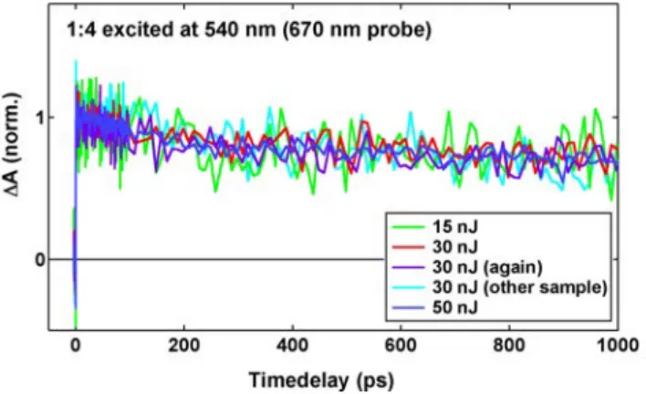
ensuring for each sample the complete absence of 1) intensity effects by comparison to the (identical) dynamics at slightly higher and lower power, and 2) degradation. An example is given in Figure S1, which shows identical normalized dynamics measured at lower and higher pump energy than the used 30 nJ, as well as for two consecu-tive scans and for another sample of similar composition.
Figure S1. Example showing the reproducibility of the TA dynamics of a 1:4 sample excited at 540 nm and
S3
The probe beam for the TA measurements consisted of a white light continuum (400-1050 nm), generated by
passing a portion of the 778 nm amplified Ti:sapphire output through a 5 mm thick CaF2 plate (in constant motion
to avoid burning). Either a 750 nm low pass or a 850 nm high pass filter was used to remove the remaining fun-damental intensity from the white light. The visible and nIR parts of the spectrum were thus recorded separately. The probe intensity was always less than the pump intensity (< 10 nJ) and the spot size was much smaller (about 0.2 mm). The probe pulses were time delayed with respect to the pump pulses using a computerized translation stage. The probe beam was split before the sample into a signal beam (transmitted through the sample and crossed with the pump) and a reference beam. The signal and reference were detected with a pair of 163 mm
spectro-graphs (Princeton instruments, SpectraPro 2500i) equipped with a 512×58 pixels back-thinned CCD (Hamamatsu
S07030-0906) and assembled by Entwicklungsbüro Stresing, Berlin. To improve sensitivity, the pump light was chopped at half the amplifier frequency, and the transmitted signal intensity was recorded shot by shot. It was corrected for intensity fluctuations using the reference beam. The transient spectra were averaged until the desired signal-to-noise ratio was achieved (5000-6000 shots). The polarization of the probe pulses was at magic angle relative to the pump.
All TA spectra were corrected for the chirp of the white-light probe pulses. Dynamics corresponding to differ-ent probe wavelengths were obtained by taking cross sections through the chirp-corrected TA spectra recorded at about 350 different time delays in the -1 ps to 1 ns range. They were analysed globally, i.e. using the same time
constants for the simultaneous analysis of the TA dynamics taken every 5 nm throughout the spectrum.2 We have
chosen not to impose any specific model on our results, but instead to globally fit multiexponential functions to the dynamics, despite that there might not be a direct physical meaning to using such functions. Nevertheless, the multiexponential analysis perfectly suits the purpose for the level of analysis required here. It allows estimating the time scale on which a process is occurring. Moreover, the sign of the pre-exponential factor indicates whether the process associated with the time constant leads to a rise or a decay of the TA signal at a given probe wave-length. By plotting the pre-exponential factors as a function of probe wavelength (yielding amplitude spectra), the evolution of different signatures in the TA spectrum can be correlated at one glimpse.
Electro-Absorption Spectroscopy.
The electro-absorption (EA) spectra were obtained in reflectance mode on full solar cell devices with a compa-rable setup as described for the TA experiments, with the probe beam passing through the ITO, the active layer and then being reflected off the aluminium electrode. The white light probe (400-700 nm) was generated in a 3 mm sapphire disc from the 778 nm output of an amplified femtosecond laser (the same as described in the TA section). A 750 nm low pass and a bandpass filter (315-750 nm) were used to remove the residual 778 nm. The probe beam was split before the sample into a signal beam (focused on the sample and reflected off the alumini-um electrode into the detector) and a reference beam reaching a second detector. The signal and reference were
detected with a pair of 163 mm spectrographs (Andor Technology, SR163) equipped with a 512×58 pixels
back-thinned CCD (Hamamatsu S07030-0906) and assembled by Entwicklungsbüro Stresing, Berlin. A similar shot-by shot detection scheme as for the TA spectroscopy was implemented, but this time the electric field applied across the solar cell with a function generator (Tektronix AFG 2021) was modulated. Thus, a square voltage pulse (up to
6V) in reverse bias (100 μs duration) was applied at half the probe frequency of 1 kHz, and the reflected probe
light was measured shot-by-shot in the presence and in the absence of electric field, averaged over 3000 shots.
Fluorescence Up-Conversion Spectroscopy.
The time-evolution of the fluorescence from the pBTTT and pBTTT:PCBM films was measured on the femto-second time scale using the fluorescence up-conversion technique. The setup, based on a modified FOG100
sys-tem (CDP Lasers & Scanning Syssys-tems), has been described in detail elsewhere,3 except that a Mai Tai HP
(Spec-tra-Physics) mode-locked Ti:sapphire laser system was used to have a tunable excitation wavelength. Its 800 nm or 1000 nm output (100 fs pulse duration, 80 MHz repetition rate) was frequency doubled for sample excitation at
400 nm or 500 nm, respectively. The pump intensity per pulse was about 4 mW, yielding a fluence of 3 µJ/cm2
(with a spot diameter of 50 µm). Any intensity effects were negligible. The measured sample fluorescence was
enhanced by sum-frequency generation with a delayed gate pulse in a non-linear BBO crystal. Phase matching conditions were tuned in order to probe the fluorescence dynamics at different emission wavelengths. The up-converted signal was then dispersed in a monochromator and its intensity measured with a photomultiplier tube operating in the photon counting mode. The polarization of the pump beam was at magic angle relative to that of the gate pulses. To minimize degradation, the encapsulated samples were continuously rotated during the
up-S4
conversion measurements. At least three scans of the dynamics in the -5 ps to 1000 ps range were averaged at each emission wavelength. No degradation of the samples was observed between scans. For each sample, the normalized fluorescence time profiles obtained at various emission wavelengths were analyzed globally by ad-justing a trial function to the measured data points using a nonlinear least-squares fitting procedure. The dynamics could in all cases be well reproduced by the convolution of a Gaussian-shaped instrument response function (IRF) with the sum of several exponential terms. The analytical expression for this function has been described
else-where.4 The width of the IRF was found to be around 100 fs.
2. Additional Structural Data
Figure S2. Electron spectroscopic images (ESI) of pBTTT:PCBM (top), pBTTT:Me7:PCBM (middle) and
pBTTT:Me12:PCBM (bottom) films, illustrating that addition of 10 molar equivalents of the additives causes the fullerene and polymer to phase separate. The density difference we observe indicates average variations of 50 nm and 100 nm in pBTTT:Me7:PCBM and pBTTT:Me12:PCBM, respectively, although smaller domains are likely to be present. Three distinct phases can be distinguished: sulphur rich domains (polymer-rich; green), carbon rich domains (fullerene-rich; red) and strongly intermixed phase (co-crystal-phase; yellow). Essentially no phase con-trast is obtained for pBTTT:PC61BM film cast at 35 °C, illustrating that the binary is finely intermixed.
S5
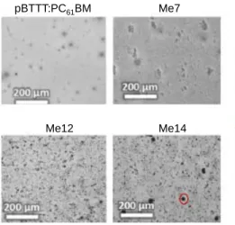
Figure S3. Visible light microscope images of pBTTT:PCBM, pBTTT:Me7:PCBM (Me7), pBTTT:Me12:PCBM
(Me12) and pBTTT:Me14:PCBM (Me14), all containing 10 molar equivalents of the additive. The presence of additives increases the surface roughness of the films and leads to large fullerene domains (the visible black spots), when long chain additives such as Me12 and Me14 are used. Via scanning transmission X-ray microscopy (STXM) absorbance measurements, these domains can be identified as PCBM-rich (see Buchaca-Domingo et al., Mater. Horiz. 2014, 1, 270; ref. 24 in the main text).
3. Verification of the PCBM Content in the Me 12 Blend
Figure S4. Steady-state absorption spectra of the 1:1 (35°C), the Me 7 (1:10:1) and the Me 12 (1:10:1) blends
measured as thin films and after re-dissolution of the films in chlorobenzene. We noticed a decrease of the rela-tive PCBM absorption below 400 nm for the samples containing 10 molar equivalents of Me 12 or Me 14 (see main text), although the amount of fullerene used in the film processing was the same as for the 1:1 and Me 7 samples. To verify that the PCBM was still present in those blends, we re-dissolved the Me 12 sample in chloro-benzene, and indeed recovered the fullerene absorption to the same level as in re-dissolved 1:1 and Me 7 blends.
pBTTT:PC61BM Me7 Me12 Me14 Energy (eV) Absorbance (OD) Absorbance (OD) Energy (eV) pBTTT PCBM pBTTT:PCBM pBTTT PCBM Me14 284 288 292 296 350 400 284 288 292 296 350 400 0.5 1.0 1.5 2.0 2.5 3.0 0.2 0.3 0.4 0.5 0.6 0.7 0.1
S6
4. Additional TA Data with 390 nm Excitation
Figure S5. TA spectra at selected time delays for the 1:1 (35°C and RT) and 1:4 pBTTT:PCBM blends following
excitation at 390 nm. Thicker solid lines are smoothed and overlaid to the raw experimental data.
5. Amplitude Spectra for the 1:1 and 1:4 Blends
Figure S6. Amplitude spectra associated with the time constants (shown in the legend) obtained by
multi-exponential global analysis of the TA dynamics for the fully intercalated 1:1 (35°C) and 1:4 (35°C) sample, ex-cited at 390 or 540 nm. Thicker solid lines are smoothed and overlaid to the raw experimental data.
S7
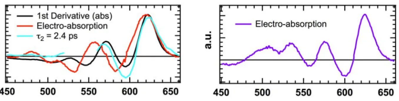
6. Enlarged Insets of Figure 5A and 5C from Main Text
Figure S7. The left panel shows the first derivative of the steady-state absorption spectrum (black), the
electro-absorption spectrum measured on a solar cell with an applied bias of 6 V (red), and the amplitude spectrum asso-ciated with the 2.4 ps time constant obtained by global analysis of the TA data with 540 nm excitation (cyan), all measured for the 1:1 pBTTT:PCBM film (by weight) processed at 35 °C (fully intercalated). The right panel shows the electro-absorption spectrum measured on a solar cell with an applied bias of 6 V (violet), for the 1:4 pBTTT:PCBM film (by weight) processed at 35 °C (co-crystalline phase and neat PCBM clusters).
7. Electro-Absorption Data for Neat pBTTT and the 1:1 Blend
Figure S8. (A) Electro-absorption spectra measured on solar cell devices of neat pBTTT and the intercalated 1:1
(35°C) pBTTT:PCBM blend, with 6V applied bias. (B) Quadratic dependence of the EA amplitude at 620 nm as a function of externally applied voltage bias. There is indication that the EA spectrum of neat pBTTT is weaker and less sharp than for the 1:1 blend (although a precise quantitative comparison is not possible because the film thickness and absorbance could not be rigorously controlled). We also note that, due to batch-to-batch variability, the absorption spectra of the films used for the EA spectroscopy were slightly different compared to the ones used for the TA experiments. In particular, the spectrum of neat pBTTT had a slightly more pronounced shoulder on its red side, which might explain the slightly enhanced EA band at 620 nm, not seen in the TA experiments.
S8
8. Molecular Structure of the pBTTT:PCBM Co-Crystal
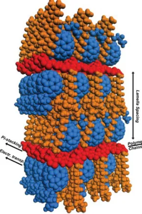
Figure S9. Space-filling structure of a pBTTT:fullerene co-crystal, based on the simulated unit cell. The polymer
backbones, polymer side chains and fullerene molecules are red, orange and blue, respectively. Reproduced with permission from Ref. S5. Copyright © 2012 WILEY-VCH Verlag GmbH & Co. KGaA, Weinheim.
9. Electrostatic Simulations
In order to better understand the evolution of the EA signature observed in our TA data, we used simple electro-static considerations applied to the particular geometry of the pBTTT:PCBM co-crystal phase. The EA signature most visible in the TA spectra (600-650 nm region) results from transitions in pBTTT, while the weaker contribu-tion of PCBM is masked by the GSB of the polymer. We will therefore limit the discussion to the EA induced in the polymer chains by photo-generated charges. Since the local field generated by a point charge decays with
distance according to 1/a2 (and E2 decays even faster with 1/a4), only the pBTTT chromophores located in closest
proximity to a charge will experience a significant Stark effect. By inspection of the crystal structure shown in Figure S9, those are the ones located on both sides of the positive charge (hole) on the same chain, and the ones
on the chains π-stacked above and below the hole. The field created by the hole across the lamella spacing of ~3
nm is much weaker. Similarly, we neglect the effect of the field generated by the negative charge (electron) on the pBTTT chromophores, as this will mainly affect the close-by fullerene molecules. We treat the charges as point charges and do not take into account their delocalization in the PCBM clusters or polymer chromophores.
In its proximity, the positive charge will dominate the field experienced by neighboring chromophores. When the hole can be considered as a free charge (i.e. when the electron is sufficiently far), the electric field around the hole will radiate outwards uniformly in all directions (a is the distance from the charge, q is the unit charge
(1.6·10-19 C) and
ε0 is the permittivity of free space (8.85·10-12 As/Vm, we did not correct for polymer medium)):
E+free = q 4
πε0
1 a2 ! " # $ % &S9
When the electron approaches the hole, it will influence the field around the positive charge depending on how close it is (the distance between charges is denoted as d). By using vector addition, we will calculate the magni-tude of the electric field as a function of d in the vicinity of the positive charge (the EA scales with the square of this field, thus its direction does not matter). We consider positions A and B (aligned with the dipole formed by the two charges, looking either between the charges or on the other side of the hole), as well as position C (in the plane perpendicular to the dipole). Finally, position D is also perpendicular to the dipole, but in the plane taken in the middle of the two charges:
The fields due to the positive and negative charge point in opposite directions, which means that they will par-tially cancel. When the electron-hole distance approaches zero, the field experienced on the outside of the dipole vanishes. As the negative charge moves further away, the field at position A increases until it reaches the value corresponding to the free positive charge.
EAtot = q 4
πε0
1 a2 − 1 d+a(
)
2 " # $ $ % & ' 'Figure S10 A
The fields due to the positive and negative charge point in the same direction, so the total field will be enhanced inside the dipole. The effect of the negative charge is greater than in case A, because position B is closer to it. Looking at the dependence on a (distance from the hole), the magnitude of the field first decreases going away from the positive charge and increases again when approaching the negative charge. As the distance d between the charges increases, the field between them becomes smaller and tends to the value of the free hole.
E
totB=
q
4
πε0
1
a
2+
1
d
− a
(
)
2⎛
⎝⎜
⎞
⎠⎟
1.0x10⁹ 0.8 0.6 0.4 0.2 0.0 Electric field (V/cm) 1.0 0.8 0.6 0.4 0.2 Distance a (nm) d = 0 nm d = 0.2 nm d = 0.5 nm d = 1 nm d = 2 nm d = 5 nm d = inf Position AS10
Figure S10 B
The fields due to the positive and negative charge are almost perpendicular. The effect of the negative charge is to weakly tilt the field in its direction and to slightly reduce its magnitude. Close to the hole (when a is small), the perturbation caused by the negative charge is much less pronounced than in positions A and B. It becomes more pronounced with increasing a. As in case A, the field at position C vanishes when the distance d between the charges tends to zero, and increases with d towards the value of the free hole.
E
C tot=
q
4
πε0
1
a
2−
a
a
2+
d
2(
)
3/2⎛
⎝
⎜
⎜
⎞
⎠
⎟
⎟
2+
d
a
2+
d
2(
)
3/2⎛
⎝
⎜
⎜
⎞
⎠
⎟
⎟
2 Figure S10 CWe are now looking at the plane in the middle of the charges (so that a is no longer the distance from the posi-tive charge, but the distance from the centre of the dipole). The fields due to the posiposi-tive and negaposi-tive charge cancel in the direction perpendicular to the dipole, but add up in the direction aligned with it. There is overall an increase of the total field magnitude, which is very important when the distance d between the charges is small, but drops rapidly to the value of the free charges as d is increased. The field in positing D due to free charges is small, because D is far away from either charge. For a small electron-hole separation, there is a quite shallow distance dependence on a, which means that even chromophores a little further away can be affected by the field.
1.0x10⁹ 0.8 0.6 0.4 0.2 0.0 Electric field (V/cm) 1.0 0.8 0.6 0.4 0.2 Distance a (nm) d = 0.5 nm d = 1 nm d = 2 nm d = 5 nm d = inf Position B 1.0x10⁹ 0.8 0.6 0.4 0.2 0.0 Electric field (V/cm) 1.0 0.8 0.6 0.4 0.2 Distance a (nm) d = 0 nm d = 0.2 nm d = 0.5 nm d = 1 nm d = 2 nm d = 5 nm d = inf Position C
S11
E
totD=
q
4
πε0
d
d
24
+
a
2⎛
⎝⎜
⎞
⎠⎟
3/2 Figure S10 DImplications for the evolution of the EA signature
Electron-hole pairs that are generated within the intimately mixed co-crystal phase are geometrically forced to be close and are presumably significantly bound (Figure S9). The dipole formed by the charge pair is perpendicu-lar to the pBTTT backbones (Figure 2C of the main text). As discussed above, the polymer segments closest to the hole, which will dominate the EA response, are the ones located on both sides of the positive charge on the
same chain, and the ones on the chains π-stacked above and below the hole. They are thus all in position C with
respect to the electron-hole dipole (in the plane perpendicular to it). There are no polymer segments between the two charges (position B), and the ones in position A are separated by the lamella spacing distance, and thus too far away to significantly contribute to the EA. There might be some contribution from position D, if the polymer chains are not perfectly straight. Assuming an initial charge separation distance (d) of 1 nm (which is reasonable based on the size and arrangement of the pBTTT and PCBM molecules), the field at position C is significant and explains the presence of the EA signature in the TA spectra of fully intercalated samples at early time delays (Figure S10 C). In fact, the neighboring polymer segments at position C, located at a distance (a) of about 0.2-0.5 nm away from the hole, experience an electric field very close to the one that would be created around a free hole (i.e. the influence of the electron is small, see Figure S11). The early EA signature form charges promptly gener-ated in the co-crystal phase should therefore have comparable amplitude to the one expected for separate charges.
Figure S11
In the fully intercalated 1:1 blend (only co-crystal phase present), there is a weak decay of the EA signal with a time constant of 2.4 ps (see main text). This could be related to relaxation of the charges (for example a change in the extent of delocalization of the hole), or to migration of some charges (which do not geminately recombine) within the co-crystalline region. Considering Figure S9, the holes can migrate along the polymer chains or along the π-stacks (the former is probably favored), while the electrons can only migrate in the direction parallel to the
1.0x10⁹ 0.8 0.6 0.4 0.2 0.0 Electric field (V/cm) 1.0 0.8 0.6 0.4 0.2 Distance a (nm) d = 0.2 nm d = 0.5 nm d = 1 nm d = 2 nm d = 5 nm d = inf Position D
S12
π-stacks (because they are hindered in the other directions by the polymer backbones and side-chains). In any
case, there will not only be an increase of the electron-hole distance (d) as the charges separate, but the dipole will also rotate with respect to the frame of the co-crystal, so that neighboring molecules will find themselves in positions A, B, C and D (instead of only C and maybe D). It is difficult to quantitatively estimate the overall ef-fect of the total experienced field in view of the dipole separation and rotation. The observed weak decay of the EA can nevertheless be rationalized by taking into account mainly position D (which affects segments even quite far away from the dipole), and where the field decreases most steeply as the charges separate (Figure S10 D and S11).
For the 1:4 blend, additional fullerene clusters are present, which drive the electrons towards them, thus favor-ing spatial charge separation and preventfavor-ing geminate charge recombination. For the partially intercalated three-phase microstructures (e.g. obtained with Me 7), there are also neat pBTTT domains present, which will most probably attract the holes towards them. The systems therefore evolve from a situation where the EA stems from an electron-hole pair in the co-crystal phase, to a situation where it stems from a free hole, which either remains in the co-crystal phase (1:4 blend) or has migrated to a free pBTTT domain (Me 7). As shown in Figure S11, once the hole is separated by about 5 nm from the electron it can be considered as free, and the electric fields in posi-tions A, B and C become equal, while the contribution of position D has vanished. We have seen above that the EA amplitude for a charge pair in the co-crystal geometry (mainly from position C) is very comparable to the one expected for a free hole. Therefore, the migration of the charges to neat domains should not significantly affect the evolution of the EA signature, except for the weak reduction already observed in the 1:1 blend (due to relaxa-tion and posirelaxa-tion D). This is indeed the case for the 1:4 blend, but the EA signature completely vanishes within < 1 ps for the three-phase microstructure of the Me 7 sample. The fast EA decay in this sample is related to the
nature of the polymer segments surrounding the free hole, i.e. to the much weaker EA caused by polymer
seg-ments in the neat domains compared to polymer segseg-ments in the co-crystal phase (see main text). When charges are generated at the domain boundaries of neat phases by delayed electron and hole transfer in the partially inter-calated or predominantly phase separated blends processed with Me 7, Me 12 and Me 14, the hole is also found in neat pBTTT domains, explaining the observed absence of the EA signature.
10. References
(S1) Mcculloch, I.; Heeney, M.; Bailey, C.; Genevicius, K.; I, M.; Shkunov, M.; Sparrowe, D.; Tierney, S.; Wagner, R.; Zhang, W. M.; Chabinyc, M. L.; Kline, R. J.; Mcgehee, M. D.; Toney, M. F. Nat. Mater. 2006, 5, 328.
(S2) van Stokkum, I. H. M.; Larsen, D. S.; van Grondelle, R. BBA-Bioenergetics 2004, 1657, 82.
(S3) Morandeira, A.; Engeli, L.; Vauthey, E. J. Phys. Chem. A 2002, 106, 4833.
(S4) Furstenberg, A.; Vauthey, E. J. Phys. Chem. B 2007, 111, 12610.
(S5) Miller, N. C.; Cho, E.; Junk, M. J. N.; Gysel, R.; Risko, C.; Kim, D.; Sweetnam, S.; Miller, C. E.; Richter, L. J.; Kline, R. J.; Heeney, M.; McCulloch, I.; Amassian, A.; Acevedo-Feliz, D.; Knox, C.; Hansen, M. R.; Dudenko, D.; Chmelka, B. F.; Toney, M. F.; Brédas, J.-L.; McGehee, M. D. Adv. Mater. 2012, 24, 6071.