HAL Id: hal-03052274
https://hal.archives-ouvertes.fr/hal-03052274
Submitted on 10 Dec 2020
HAL is a multi-disciplinary open access
archive for the deposit and dissemination of
sci-entific research documents, whether they are
pub-lished or not. The documents may come from
teaching and research institutions in France or
abroad, or from public or private research centers.
L’archive ouverte pluridisciplinaire HAL, est
destinée au dépôt et à la diffusion de documents
scientifiques de niveau recherche, publiés ou non,
émanant des établissements d’enseignement et de
recherche français ou étrangers, des laboratoires
publics ou privés.
Backscatter Internet-of-Things
Karan Gumber, Corinne Dejous, Simon Hemour
To cite this version:
Karan Gumber, Corinne Dejous, Simon Hemour. Harmonic Reflection Amplifier for Widespread
Backscatter Internet-of-Things. IEEE Transactions on Microwave Theory and Techniques, Institute
of Electrical and Electronics Engineers, In press, �10.1109/TMTT.2020.3038222�. �hal-03052274�
IEEE TRANSACTIONS OF MICROWAVE THEORY AND TECHNIQUES 1
Abstract— The highly power-efficient Backscattering communication scheme holds solid potentials to lead the Internet of Things technologies. However, the asymmetric radio frontend architectures that ensure cheap and pervasive communicating things and tags at one end of the link, overburdens the other end of the link ("reader") with complicated and expensive hardware. This turns out to prevent the integration of the technology in the wide spectrum of consumer electronic devices (e.g. RF smartphone platforms). By separating TX and RX frequency bands, harmonic backscattering scheme drastically loosens the technological constraints towards integration. We propose here the use of a single tunnel diode to build a harmonic reflection amplifier (HRA), using the non-linear behavior of the negative differential resistance region to both generate harmonics and amplify the signals. The circuit also behaves like a common backscatter, with same-frequency backscattering modulation for operation with legacy readers. Operating below 150mV, the HRA drains 144µW dc power with a measured positive conversion gain of 18dB.
Index Terms— Backscatter radio, harmonic reflection
amplifier, RFID, self-interference, tunnel diode. I. INTRODUCTION
ITH the emergence of the fifth generation (5G) technologies, the year 2020 came across 30 billion connected devices, or 5.1 connected devices per person on average [1], which anticipates a proliferation of Internet-of-Things (IoT) platforms that could range from small portable electronics devices such as smartphones and sensors to large electric vehicles. Backscatter communication is a promising technology towards true ubiquitous IoT, as it simplifies the many “thing” complexity [2]. In this asymmetric communication scheme, RF signal is generated on one side only (the reader), whereas the tag backscatters the modulated signal to the reader with identification and other preferred information [3].
Most readers work in monostatic configuration where a transmitter (Tx) and receiver (Rx) share the same antenna. The low Tx to Rx isolation resulting from contiguous intra-band
operation leads to self-interference (SI) or self-jamming signal leakage. Unfortunately, the anti-jamming interference circuits and/or high dynamic radio front end that have to be used to circumvent SI are expensive [4]. Self-jamming mitigation can either use interference from directional coupler [5] or quasi-circulator [6]. Substantial methods have been employed, including LNA post-distortion [7], feed-forward cancellation [8], and impedance tuning [9].
In [10], the mitigation of SI in monostatic configuration is done by using a directional coupler with impedance mismatch reflector incorporated into the antenna. Similarly, the anti-jamming signal in [11] has been achieved with the combination of power divider, combiner and vector multiplier. However, the performance of this method is entirely dependent on the dynamic range of vector multiplier. To cancel the leakage signal in [12], a compensation signal was generated using an ultra-wideband poly-phase power divider, which is added vectorially before the receiver front end. Signal conditioning has been used in [13], in which a sample of Tx signal is combined with an Rx signal with opposite phase to counter the SI. The adaptive SI cancellation algorithm was discussed in [14] that automatically alters the self-jamming signal depending upon the changes in the tag environment.
All these methods provide rejection of the Tx leakage, but at the cost of increased reader Rx complexity. These solutions are also bulky in physical size and simultaneously limit the sensitivity of the system.
An alternative technique to reduce self-jamming is separating the Tx/Rx frequencies, similar to the frequency-division duplex system. The Tx leakage that influences the Rx frequency is filtered at Tx output, conversely, the leakage outside the Rx frequency is filtered at Rx input. Therefore, in the recent years, alternative solutions have been exploiting passive transponders/tags [15], [16] to generate harmonics for enabling communication that greatly reduces direct reflections and self-interference. The idea has even been proposed for active [17] circuit. However, dual-band operation is not new and have been explored for the RFID transponder [18]-[20], but the generation of harmonics comes at a cost of conversion loss that significantly impact the link budget, and thus the communication distance. Table I and Fig. 1 compare the proposed outcome with the previously reported reflection amplifier in terms of power consumption, gain and power added efficiency (η) (PAE) etc. [21]-[40], while Table II compares the performance of the proposed harmonic backscatterer with
Harmonic Reflection Amplifier
for Widespread Backscatter Internet-of-Things
Karan Gumber, Member, IEEE, Corinne Dejous, Member, IEEE and Simon Hemour, Senior Member,
IEEE
W
Manuscript submitted on July 21, 2020; revised October 27, 2020. This work was supported in part from the French State in the frame of the “Investments for the future” Programme IdEx Bordeaux, reference ANR-10-IDEX-03-02, and LabEx AMADEus (ANR-10-LABX-0042-AMADEUS). (Corresponding authors: K. Gumber; S. Hemour.)
K. Gumber, C. Dejous, and S. Hemour are with IMS Research center, Department of science and technology, University of Bordeaux, Bordeaux INP, CNRS UMR5218 Talence, France, 33400 (e-mail: [email protected],[email protected], [email protected]).
1 10 100 -120 -100 -80 -60 -40 -20 0 20 1 10 100 -120 -100 -80 -60 -40 -20 0 20 Pow er (dBm) Distance (m)
Power moving away from Tag @ 414.6 MHz -Path Loss @ 414.6 MHz
-Path Loss @ 829.2 MHz
Power moving away from reader @ 414.6 MHz
Pow
er
(dBm)
Distance (m)
Power moving away from Tag @ 829.2 MHz
[22] [23] [24] [25] [26] [27] [29] [28] [30] [31] [33] [36] [38] [39] This Work This Work: Conversion Efficiency 0.001 0.01 0.1 1 10 100 1000 0 10 20 30 40 Pdc (mW) Po wer Add ed Eff ici ency (%)
Fig. 1. Comparing the various state-of-the-art reflection amplifiers in terms of efficiency and output power vs dc power consumption.
previously reported harmonic tags [19], [41]-[46].
A harmonic tunneling tag concept is illustrated in Fig. 2, where the tunnel diode is employed as a nonlinear element. The signal illuminates the tag at the fundamental frequency (f0), and
the non-linear element in the tag generates and re-radiate the signal back to the reader, both at the fundamental frequency (f0)
and at the second harmonic (2f0).
The present study is an expanded version of [47], which proposed a topology based on a non-linear, negative resistance
TABLE II:COMPARISON OF STATE-OF-THE-ART HARMONIC BACKSCATTER
Ref. Type 2nd Harmonic Freq. (GHz) CG (dB)
This work Active 0.414>0.829 -24 to +29 [19] Passive 7 -17 [41] Passive 1.6 -26 [42] Passive Active 0.929 -15 (without amplifier) -8 (with amplifier) [43] Semi-passive 1.8 -23 [44] Passive 2.4 -26.5 [45] Passive 2 -19.9 [46] Passive 1.736 -30
based tag that can completely overshadow the SI and also provide a conversion gain of around 18 dB at 2f0 with power
consumption of 144 µW, measured at an excitation signal of -50 dBm. In addition, the HRA allows simultaneous use of both the frequency bands to enable legacy compatibility with non-harmonic readers. It also increases the throughput in a crowded frequency spectrum and thus it has emerged as a potential solution in a cluttered environment for long-range RFID tags.
The originality of the work lies in stability analysis of the proposed HRA. The concept of stability in negative resistance devices is explained theoretically and supported by simulation as well as measurement results. The capacity of the HRA to perform binary phase-shift keying (BPSK) is also elaborated in the expanded version. In addition, the effect of the incident TABLE I:COMPARISON OF STATE-OF-THE-ART REFLECTION AMPLIFIERS AVAILABLE IN LITERATURE
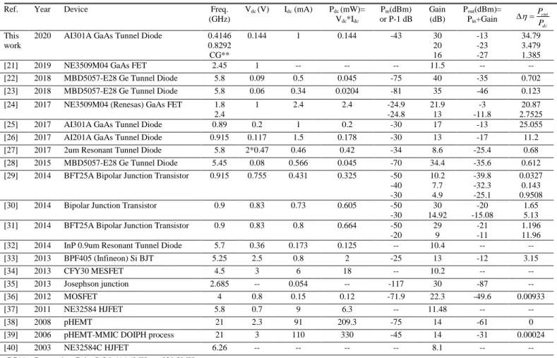
Ref. Year Device Freq.
(GHz) Vdc (V) Idc (mA) Pdc (mW)= Vdc*Idc Pin(dBm) or P-1 dB Gain (dB) Pout(dBm)= Pin+Gain out dc P P This work
2020 AI301A GaAs Tunnel Diode 0.4146
0.8292 CG** 0.144 1 0.144 -43 30 20 16 -13 -23 -27 34.79 3.479 1.385
[21] 2019 NE3509M04 GaAs FET 2.45 1 -- -- -- 11.5 -- --
[22] 2018 MBD5057-E28 Ge Tunnel Diode 5.8 0.09 0.5 0.045 -75 40 -35 0.702
[23] 2018 MBD5057-E28 Ge Tunnel Diode 5.8 0.06 0.34 0.0204 -81 35 -46 0.123
[24] 2017 NE3509M04 (Renesas) GaAs FET 1.8
2.4 1 2.4 2.4 -24.9 -24.8 21.9 13 -3 -11.8 20.87 2.7525
[25] 2017 AI301A GaAs Tunnel Diode 0.89 0.2 1 0.2 -30 17 -13 25.055
[26] 2017 AI201A GaAs Tunnel Diode 0.915 0.117 1.5 0.178 -30 13 -17 11.2
[27] 2017 2um Resonant Tunnel Diode 5.8 2*0.47 0.46 0.42 -34 8.6 -25.4 0.68
[28] 2015 MBD5057-E28 Ge Tunnel Diode 5.45 0.08 0.566 0.045 -70 34.4 -35.6 0.612
[29] 2014 BFT25A Bipolar Junction Transistor 0.915 0.755 0.431 0.325 -50
-40 -30 10.2 7.7 4.9 -39.8 -32.3 -25.1 0.0327 0.143 0.9508
[30] 2014 Bipolar Junction Transistor 0.9 0.83 0.73 0.605 -50
-30 30 14.92 -20 -15.08 1.65 5.13
[31] 2014 BFT25A Bipolar Junction Transistor 0.9 0.83 0.8 0.664 -50
-20 29 9 -21 -11 1.196 11.96
[32] 2014 InP 0.9um Resonant Tunnel Diode 5.7 0.36 0.173 0.125 -- 10.4 -- --
[33] 2013 BPF405 (Infineon) Si BJT 5.25 2.5 0.8 2 -25 13 -12 3.15 [34] 2013 CFY30 MESFET 4.5 3 6 18 -- 10.2 -- -- [35] 2013 Josephson junction 2.685 -- 0.054 -- -117 30 -87 -- [36] 2012 MOSFET 4 0.8 0.15 0.12 -71.9 22.3 -49.6 0.00933 [37] 2011 NE32584 HJFET 5.8 0.7 9 6.3 -- 11.48 -- -- [38] 2008 pHEMT 21 2.3 91 209.3 -75 14 -61 0
[39] 2006 pHEMT-MMIC DOIPH process 21 3 110 330 -45 14 -31 0.00024
[40] 2003 NE32584C HJFET 6.26 -- -- -- -- 8.1 -- --
IEEE TRANSACTIONS OF MICROWAVE THEORY AND TECHNIQUES 3 T u n n el D io d e Matching Network L 2 C1 L 1 DC Block RFin@f0 RFout@f0 RFout@2f0 R F b loc k C2 Vbias DC Biasing and Stabilization L 3 Cancellation circuit-less reader (separate Tx and Rx frequency) Fig. 2. The harmonic tunneling RFID dual-band communication system that is able to communicate at fundamental and harmonic frequency.
power on the reflection gain, conversion gain and input impedance of the HRA are experimentally demonstrated. The impedance characterization of the AI301A bare tunnel diode in the simulations and measurements has been carried out.
The paper is organized in five sections: Section II provides the details on the characterization of bare tunnel diode, while Section III and IV demonstrate the measurement results based on static and dynamic-bias modulation, respectively. Finally, based on analysis and preceding results, conclusions are made in Section V.
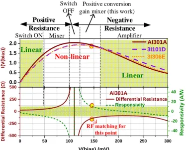
II. CHARACTERIZATION OF A BARE TUNNEL DIODE The first step before fabricating any prototype based on tunnel diode is to determine the dc current-voltage (IV) characteristic of the bare tunnel diode. The dc IV characteristics of the three tunnel diodes (AI301A, 3I101D and 3I306E) are shown in Fig. 3, they were measured over a bias voltage (Vb)
ranging from 0 mV to 300 mV. The differential resistance and current responsivity [48] of AI301A are also shown in Fig. 3. Table III shows a comparison of these three diodes based on spice parameters, each with its biasing voltage and the corresponding negative.
As depicted from the IV curve, the tunnel diode AI301A shows a negative differential resistance (NDR) region from 110 mV to 300 mV, where the output current starts reducing with the increase in Vb. When biased in the NDR region, the tunnel
diode can operate as an amplifier. For a given dc bias (meaning dc power loss), a positive differential resistance would dissipate RF power (RI2), while a negative differential resistance would
increase RF power (-RI2) and this property makes it different
from other diodes.
For these measurements, the E3648A high precision biasing supply from Keysight is used to bias the diode, which was controlled using the Command Expert, Standard Commands for Programmable Instruments. For high precision extraction of voltage and current consumption of AI301A tunnel diode, 34410 and 34401 digital multi-meters (DMM) are employed. The number of power line cycles (PLC) of 34410 DMM is set at 10 and 34401 DMM is set at 6 digits slow, which corresponds to 100 PLC integration time and 6.5-digit resolution. The biasing voltage across the diode is varied from 1mV to 300mV at a step of 1mV, and the delay between two consecutive steps is set to 3 sec. 𝐼(𝑣) = ∑𝑖=𝑁𝑖=0𝑎𝑖𝑣𝑖, 𝑁 𝜖 ℕ. (1) Positive Resistance Negative Resistance Switch ON Linear Non-linear Linear Mixer Switch OFF Amplifier Positive conversion gain mixer (this work)
0.0 0.5 1.0 1.5 2.0 I(V(b ias )) AI301A 3I101D 3I306E 0 50 100 150 200 250 300 -500 -250 0 250 500 AI301A Diffrential Resistance:1/i'(Vbias) Responsivity:i''(Vbias)/2i'(Vbias) V(bias) (mV) Diff rent ial Res ist an ce ( Ω ) -40 -20 0 20 40 Resp on siv ity (A/W)
1
RF matching for this point 0.0 0.5 1.0 1.5 2.0 I(V(b ias )) AI301A 3I101D 3I306E 0 50 100 150 200 250 300 -500 -250 0 250 500 AI301A Diffrential Resistance Responsivity V(bias) (mV) Diff rent ial Res ist an ce ( Ω ) -40 -20 0 20 40 Resp on siv ity (A/W) D if fe re nt ia l R es is ta nc e ( ) Differential Resistance I( V (bi a s))Fig. 3. Measured dc characteristics of the tunnel diodes AI301A, 3I101D and 3I306E. The 7th order polynomial fitting of the measured dc IV characteristic allowed to estimate the differential resistance of AI301A |-Rtd|= 147 Ω and the
responsivity ℜ= 11.9 A/W that are highlighted, for biasing at 144 mV. Shaded region represents linear characteristics, where ℜ ≤│7.5 │A/W.
TABLE III:PERFORMANCE COMPARISON OF THREE DIFFERENT TUNNEL DIODES Parameters Circuit I- AI301A Circuit II-3I101D Circuit III-3I306E Vbias (mV) 144 214 164.5 I(Vbias) (mA) 1 0.68 1.073
Power consumed (uW) 144 145.5 176.5
Negative resistance -147 -158 -137
Peak current @25°C 1.6 – 2.4 mA 1.7 – 2.4mA 1.8 – 2.2mA
Voltage at peak current <180mV <160mV <170mV
Parasitic capacitance < 12 pF 2.5 – 10pF 4 – 12pF
Parasitic inductance <1.5nH <1.3nH NA
technology GaAs GaAs GaAs
The 7th order polynomial fitting was extrapolated [49]:
𝐼(𝑣) = −5.83𝑣7+ 14.12𝑣6− 12.87𝑣5+ 5.10𝑣4−
0.53𝑣3− 0.18𝑣2+ 0.04𝑣 − 1.47 ∙ 10−5 (2)
Over the negative Rtd region (Fig. 3) the device exhibits a
peak-valley voltage (ΔV) and current (ΔI) difference of around 190 mV and 1.62 mA, respectively, which sets the maximum RF “output” power of the diode to about -12 dBm, as calculated from [50]:
max 3 16
P V I (3) Frequency multiplication can be obtained when the NDR
varies nonlinearly with the voltage. The optimum doubler efficiency can be obtained, when the diode is biased at the edge of the NDR region, as the IV characteristic is almost symmetrical at the bias point [51] and the current responsivity is high. Alternately, biasing the device at the NDR midrange, anti- symmetrical around the bias point, with a constant value of Rtd and lower responsivity absolute value, would lead to
highest tripling efficiency. In this work, aiming a doubler amplifier, the bias point was chosen as 144 mV, |-Rtd|= 147 Ω.
Operating on the peak current, Vb = 110 mV, |-Rtd| >1500 Ω,
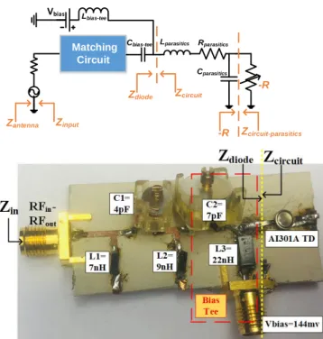
Zantenna Zcircuit-parasitics -R Matching Circuit Zdiode Zcircuit Zinput -R Vbias Cparasitics Rparasitics Lparasitics Lbias-tee Cbias-tee
Fig. 4. A fundamental block diagram and fabricated prototype of a harmonic reflection amplifier.
III. HARMONIC TUNNELING TAG STATIC MEASUREMENT The measurement campaign aimed to experimentally validate the capacity of harmonic tunneling tag in terms of achievable reflection gain at the fundamental frequency and conversion gain at the second harmonic. The basis of any measurement relies on its simulation framework, which is elaborated first. A. Simulation framework
The simulation work of the proposed design is carried out in the Advance Design System (ADS) by building the Symbolically Defined Device (SDD) model of tunnel diode from its IV characteristics. The transient simulations are performed to make sure that the HRA does not start to oscillate at any biasing voltage. The matching network was built to obtain the desired output signal at the frequency of interest. The matching network includes a dual-band LC resonator indicated in Fig. 2. The matching network performs two functions (a) make sure that the negative impedance of the diode is successfully transformed into antenna impedance (b) ensure the selectivity of desired dual-frequency band. The negative resistance seen towards the diode is -147 Ω, and the input impedance of the HRA is approx. -49 Ω, when the incident power is -60dBm. This impedance transformation is carried by the matching circuit to ensure stability as well as to transfer maximum power.
The simulated S-parameters of the full circuit (excluding diode) are shown in Fig. 5. The circuit has been optimized to exhibit negative resistance at only 450 MHz and 900 MHz frequencies. Simulation is then compared to S1P (one-port S parameter) measurements of the physical tunnel diode at the optimum bias point.
The performance of the overall HRA is characterized by reflection gain, which is given as:
0 200 400 600 800 1000 -50 -40 -30 -20 -10 0 Magnitude (dB) Frequency (MHz) S11 S21
Fig. 5. Simulated S parameter of circuit without tunnel diode, representing two resonances at the desired frequency band.
2 2 diode circuit in diode circuit Z Z Z Z (4) where Zcircuit is the load impedance connected to the reflection
amplifier. Note that the Zcircuit should also consider the antenna
impedance at the input port; Zdiode is the input impedance of the
tunnel diode (Fig. 4). The reflection gain of HRA must exceed unity as the input resistance of tunnel diode is negative [53]. If Zdiode approaches -Zcircuit, then │Гin│2 tends to infinity.
Oscillations can start if the magnitude of negative impedance of the diode exceeds the magnitude of the positive load impedance of the circuit [54], [55]:
Re
Zcircuit
Re
Zdiode
(5) where Re[Zdiode] < 0. To avoid such uncontrolled oscillations,the load impedance magnitude of the circuit designed must be always greater than the negative impedance magnitude of diode, which is given by:
Re
Zcircuit
Re
Zdiode
0 (6) where Re[Zdiode] < 0, and the highest reflective gain is obtainedonly if |Re[Zdiode]| is kept different from Re[Zcircuit] by a very
small margin.
The simulated real and imaginary impedance of the tunnel diode SDD model at different bias points is shown in the upper graph of Fig. 6 (a) and Fig. 6 (b), respectively. A quite good agreement is observed with the measured real and imaginary impedance of the AI301A tunnel diode represented in the lower graph of Fig. 6 (a) and Fig. 6 (b).
-300 -200 -100 0 0 200 400 600 800 1000 -400 -300 -200 -100 0
Simulated Impedance using SDD model 100mV 120mV 140mV 160mV 180mV Re [Zdiode ] Frequency (MHz)
Measured Impedance of Bare Diode
100mV 120mV 140mV 160mV 180mV (a)
IEEE TRANSACTIONS OF MICROWAVE THEORY AND TECHNIQUES 5 -300 -200 -100 0 0 200 400 600 800 1000 -300 -200 -100 0
Simulated Impedance using SDD
100mV 120mV 140mV 160mV 180mV Im [ Zdiod e ] Frequency (MHz)
Measured Impedance of Bare Diode
100mV 120mV 140mV 160mV 180mV (b)
Fig. 6. (a). Real and (b) imaginary impedance of the tunnel diode at various biasing using the simulated SDD model, and measured AI301A bare diode.
In order to achieve high gain at the frequency of interest, the impedance of matching network is tuned very close to the negative input impedance of tunnel diode, while respecting the non-oscillation conditions.
B. Experimental setup
For prototyping and testing, the AI301A soviet tunnel diode is used which is cheap, rugged and easily available. It is also important to mention that more efficient tunnel diodes can operate at a lower biasing point. The experimental prototype of the proposed circuit can be seen in Fig. 4(b). It was fabricated using Rogers RO3010 substrate with thickness 1.28mm, dissipation factor 0.0022 and relative permittivity 10.2. The fabricated hardware was composed of AI301A tunnel diode, variable capacitances from Vishay, and inductors from Coilcraft.
The various components of the HRA are tuned and optimized using harmonic balance and transient simulation in ADS to ensure maximum reflection and conversion gain at fundamental and 2nd harmonic frequency, while at the same time disabling
the oscillatory conditions. The working operation of HRA is summarized in Fig. 7.
The type of operation performed by the HRA depends on the input signal. With a single frequency band at f0, which can
either be centered at 414.6 MHz or 829.2 MHz, the amplifier performs a dual-band operation, by boosting the signal at fundamental frequency f0, and at the second harmonic
frequency. In p u t O u tp u t
H
R
A
Input, F0=414.6 MHz Output, 2F0=829.2 MHz Input, F0=829.2 MHz Output, 2F0=1658.4 MHz F0 F0 2F0 Reflection Gain Conversion Gain O u tp u t Reflection Gain Reflection Gain Conversion Gain Conversion GainFig. 7. The basic working principle of the harmonic reflection amplifier.
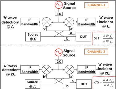
Signal Source 1X IF Bandwidth IF Bandwidth 'a' wave incident @ fn 'b' wave detection @ fn b a b Signal Source IF Bandwidth IF Bandwidth 'a' wave incident @ 2fn 'b' wave detection @ 2fn a b a b 2X CHANNEL-1 CHANNEL-2 a @ 11 @ n n b f S a f @ 2 @ n n b f CG a f Source @ fn Source @ fn DUT DUT
Fig. 8. Block diagram of one port network analysis, showing two channels with ‘a’, ‘b’ waves that measure the incident (@fn) and reflected (@fn and @2fn)
waves.
For such characterization, a one-port network analysis with frequency offset is performed (Fig. 8). Since one-port conversion gain is usually not available on vector network analyzer, it has to be computed from the raw fn a wave
(measurements @ fn with source at fn), and the 2. fn b wave
(measurements @ 2fn with source at fn). Note that special care
should be given in the calibration and error coefficient handling, as forward error term should be taken into account at fn, while reverse wave error term should be considered at 2fn.
Conversion gain for higher harmonics follow the same methodology. Practically, these measurements are done with Keysight E5080 vector network analyzer (VNA), for incident power ranging from Pin, min = -90 dBm to Pin, max = -20 dBm. C. Tuning the negative differential resistance and the conversion gain
The negative resistance of tunnel diode is exploited with respect to biasing voltage. The change in the biasing voltage tunes the negative differential resistance of tunnel diode, which in turn produces the reflection and conversion gain. The gains as a function of biasing voltage is shown in Fig. 9.
0 100 200 300 -40 -20 0 20 40 Magnitude (dB) Vbias (mV) Reflection Gain @f0414.6MHz Conversion Gain @2f0829.MHz>414.6MHz
Fig. 9. Measured reflection and conversion gain as a function of the bias voltage for an input frequency of 414.6MHz and an input power of -50 dBm.
-60 -40 -20 0 20 -80 -70 -60 -50 -40 -30 -20 -60 -40 -20 0 Zi n (o hm) Re[Z] @ f0 Im[Z] @ f0 Input Power (dBm) Re[Z] @ 2f0 Im[Z] @ 2f0
Fig. 10. Measured real (brown) and imaginary parts (green) of the HRA impedance at both frequencies f0 (=414.6 MHz) and 2f0 (=829.2 MHz) for various incident powers, when optimum bias of 144 mV is applied.
As depicted from Fig. 9, one can easily achieve the desired gain just by tuning the biasing voltage. This experiment is conducted to show the reproducibility of the measurement results across different tunnel diodes (same part number). If any other diode with the same part number is employed it can produce similar results, but may be with change in bias point. D. Frequency behavior and stability conditions
The optimum behavior of the proposed HRA is found for a bias voltage of Vb=144 mV. Under this dc condition, the
measured input impedance of the bare AI301A tunnel diode is:
27 44 @ 0=414.6 MHz 8 4 @ 2 0=829.2 MHz diode j f Z j f
To assess the overall stability of the circuit, the input impedance has to be measured as seen from the antenna to verify that there is no frequency for which it goes to the instability region. The stability test is conducted in Fig. 10, where the real impedance of the HRA is plotted against incident power. As shown in Fig. 10, when the incident power approaches near 50dBm, the HRA impedance reduces from -50 Ω towards the instability region.
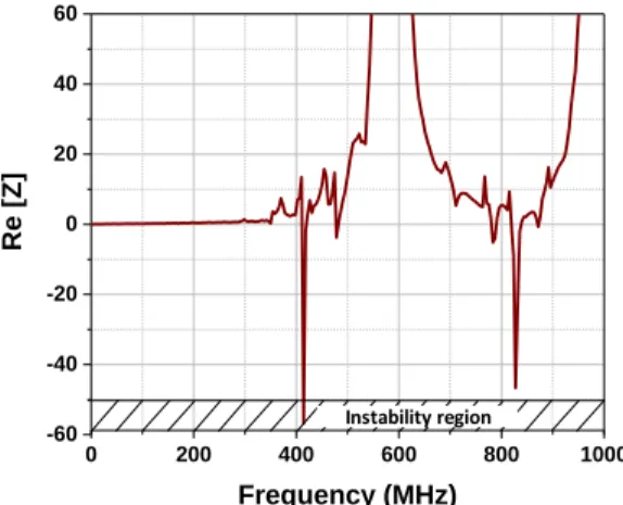
0 200 400 600 800 1000 -60 -40 -20 0 20 40 60 Re [ Z] Frequency (MHz) Instability region
Fig. 11. Measured input impedance of the HRA before final biasing for an incident power of -50 dBm, when optimum bias of 144 mV is applied. Under such conditions, self-injection locking would be expected at f0, because the impedance of the HRA falls below -50 Ω. The shaded portion represents the unstable region, if the antenna impedance (Zantenna) = 50 Ω.
10 25 50 100 250 -10j 10j -25j 25j -50j 50j -100j 100j -250j 250j +5dB +30dB +20dB Reflection Gain (dB) Unstability region +10dB
Fig. 12. Contour chart of the reflection gain (eq. 4) and stability criteria (eq.5) for a source-pull calculation of any possible antenna impedance considering the input impedance (47-j×1.3 Ohm) of the circuit at 414MHz for power below -60dBm.
It can also be confirmed from the Fig. 11 that shows the measured real part of the HRA impedance for an incident power of -50 dBm before final tuning. It is observed two sharp resonances with values below -50 Ω at f0, approximately -48 Ω
at 2f0. Under such condition free-running oscillation would
occur at f0, while an incident signal at the vicinity of f0 would
trigger an injection locked oscillation [56]-[58]. E. Antenna impedance impact on the operation
The antenna impedance mostly varies in practical case towards higher real impedance value because equivalent series resistance increases with the added loss of the surrounding antenna. Therefore, there is no risk for instability if the surrounding happened to impact the antenna impedance. Fig 12 shows the impact of antenna impedance on the stability of the proposed HRA. It can be observed from the contour plot, that the HRA always remains stable if the antenna impedance is higher than 50 Ω. If the antenna impedance is close to 50 Ω, it yields the maximum reflection gain (as high as 30dB)
F. Influence of the incident power on stability
As the HRA is designed to operate at a negative impedance very close to the antenna impedance, it is also necessary to verify the stability versus incident signal RF power level. It can be explained by considering Fig. 10 and Fig. 13, where Fig. 10 represents the variation of real and imaginary parts of the HRA input impedance at both frequencies as a function of the incident power level.
This can be observed in Fig. 13, which depicts the reflection gain (S11) and conversion gain of the HRA as a function of the incident power. From very low incident power (90 dBm) to -50dBm, the equivalent (linear) resistance seen by the input signal is very close to -50Ω, related to a high and constant value of S11. Note that in the case of unstable behavior, the S11 would keep rising as the incident power increases.
Furthermore, it can be observed in Fig. 13 that near -50 dBm, the reflection gains at f0 and 2f0 are maximum, as well as the
IEEE TRANSACTIONS OF MICROWAVE THEORY AND TECHNIQUES 7 * @ 414.6 fund parasitic MHz * @829.2 fund parasitic MHz 2 * @41 4.6 H parasitic MHz 2 * @82 9.2 H para sitic MH z -80 -70 -60 -50 -40 -30 -20 -40 -20 0 20 40 Ma g n it u d e ( d B ) Input Power (dBm) S11@[email protected] S11@2f0@ 829.2MHz CG@ 829.2MHz>414.6MHz [email protected]>829.2MHz
Fig. 13. Measured input reflection coefficient (S11) at fundamental frequency f0 (green), and at 2f0 (brown), and 2ndharmonic conversion gains with respect to f0 (blue) and 2f0 (orange) as a function of incident RF power.
│Re[Zdiode]│comes very close to Re[Zcircuit], that provides high
reflective gain │Гin│ as indicated in (4). Beyond -50 dBm
incident power level, the real part of the impedance at f0 and 2f0
increases from -50 Ω and mismatch takes place, (shown in Fig. 10 and Fig. 11). The higher the mismatch of real impedance, the lower the reflection and conversion gains.
Both reflection and conversion gains originate from different physical mechanisms of the tunnel diode. The conversion gain results from the fast varying input impedance, which is linked to the second order I(V) curve variation, i.e. the dc current responsivity represented in Fig. 3. Thus, the nonlinearity of tunnel diode generates the inter-modulation product and higher harmonics, which is power dependent, since more incident RF power will lead to greater impedance variation, hence more conversion. The negative input impedance of the circuit (linked to the differential resistance of the tunnel diode) is responsible for amplification of every existing signal, i.e. for the incident wave (reflection gain) as well as the generated harmonics (conversion gain).
Of course, as the frequency increases, the signal is more subject to parasitic losses which lead to lower conversion gain, as it is the case for 829.2 MHz to 1658.4 MHz conversion gain. The measurements reported in Fig. 13 are used to investigate the P1-dB and P3-dB compression points. The measured P1-dB incident power Pin-1 dB of -43 dBm at f0 and 2f0 corresponds to a
maximum linear Pout of -13 dBm and -23 dBm respectively. The one port analysis of the HRA consistent with ‘a’, ‘b’ waves at the frequency band f0 = 414.6 MHz and exploiting the
frequency offset mode with a multiplicative factor of 2 is shown in Fig. 14. The ‘a’ and ‘b’ wave centered at f0 = 414.6 MHz are
measured in Channel I corresponding to Fig. 8, whereas ‘b’ wave centered at 2f0 = 829.2 MHz is measured in the Channel
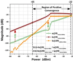
II by exploiting frequency offset mode. The data extracted from these three waves help to find the reflection and conversion gains as depicted in Fig. 15. Both ‘a’ and ‘b’ shows a very linear behavior from very low incident power (-90 dBm) to -50dBm, that imply constant reflection gain (S11) in this region.
-90 -80 -70 -60 -50 -40 -30 -20 -120 -100 -80 -60 -40 -20 0 S11=b@f0>414.6 MHz / a@f0>414.6 MHz CG=b@2f0>829.2 MHz / a@f0>414.6 MHz Ma g n it u d e ( d B ) Power (dBm) a@f0>414.6 MHz b@f0>414.6 MHz b@2f0>829.2 MHz Region of Positive Convergence -65 -22 S11 CG
Fig. 14. One port analysis of the HRA to find reflection and conversion gains from ‘a’, ‘b’ waves at fundamental frequency f0=414.6 MHz.
The conversion efficiency is given as the ratio of b@2f0/
a@f0. As it is shown in Fig. 14 when ‘b’ wave at 2f0 starts
increasing from ‘a’ wave at f0, it is marked as the region of
positive conversion gain for second harmonic that lies at 829.2 MHz. This region starts originating when the incident power impinging on the HRA comes close to -65 dBm, and it continues up to -22 dBm incident power. Similarly, this positive region of conversion gain for the 829.2 MHz fundamental frequency that corresponds to the second harmonic at 1658.4 MHz is shown in Fig. 13. This region is very small, it is only restricted to the incident power ranging from -47 dBm to -43 dBm, where the conversion gain at the second harmonic that lies at 1658.4 MHz goes above 0 dB.
Indeed, when the incident power is large enough, (here from -50 dBm), the tunnel diode ceases to operate in “small signal”, the input signal starts flowing over the positive resistance part of the curve and does not benefit further from the ideal (nonlinear & negative) response. This in turn modifies both the gain and input impedance of the HRA that pushes HRA into saturation and leads to a decrease of the gains.
It was observed that the HRA exhibits a reflection gain over the dual frequency band. The measured reflection and conversion gains for three incident powers are shown in Fig. 15. It is observed a peak reflection gain of 25 dB or even greater over both the frequency bands (f0 and 2f0) at incident power of
-50 dBm. At the same incident power, it provides a controllable conversion gain at the second harmonic of approximately 18 dB and -16.5 dB at 829.2 MHz and 1658.4 MHz, respectively. G. Selection of device
The selection of device is of concern for the fabrication of amplifier, where stability is of paramount importance. Three different diodes are shortlisted for the purpose of fabricating an amplifier, which has very similar IV characteristics as depicted in Fig. 3. After fabricating the three prototypes with three different diodes, we found the 3I101D provides excellent reflection as well as conversion gain. While, conducting the
stability test, it is unstable starting from very low power to -40dBm, which can be observed from Fig. 16. The other diode 3I306E passed the stability test as shown in Fig. 16, but was unable to provide good reflection and conversion gain. Therefore, the AI301A was chosen that has combination of both stability and efficiency. To verify the reproducibility of measurement results across different AI301A tunnel diodes (using same part number), two additional prototypes were tested using AI301A. All the prototypes tested using AI301A were very stable and produced good reflection and conversion gain.
H. Power link budget
The link budget is a method to diagnose the entire system. It determines the gain and losses in a system by calculating the RF power level at each point [59]. It governs the margin in system performance and can locate point of failure. The evaluation of the proposed system is performed in two cases shown in Fig. 17. In Case I (shown in Fig. 17 (a)), the reader and tag both transmit and receive fundamental frequency i.e. 414.6 MHz. However, in case II (shown in Fig. 17 (b)), the reader illuminates the tag at the fundamental frequency, while the tag re-radiates the second harmonic, i.e. 829.2 MHz, to the reader. The power link budget of the entire system in both cases is shown in Fig. 18, which is given as:
Pread= PT + GR + GT - LT -Pmod - LFS + GHRA (7)
all the above terms are explained in Table IV, where the value of the first five terms are assumed, the sixth term LFS is
-80 -60 -40 -20 -60 -40 -20 0 20 Re[ Z] @ f0 (ohm) Power (dBm) 3I101D 3I306E
AI301A-different part number
AI301A-different part number
AI301-used in proposed work
Instability region
Fig. 16. Measured real impedance of the HRA for three different prototypes (employing different tunnel diodes at frequency f0 (=414.6 MHz) for various incident powers.
calculated using free-space path loss (FSL) equation provided in Table IV, and the value of last term is extracted from Fig. 13. The fifth term, modulation loss (Pmod) occurs due to the change
in circuit impedance from state ‘0’ (Z= 5.6-j×0.2 Ω) to state ‘1’ (Z= –51.6-j×3.2 Ω), which defines how the tag modulates the reader signal back to reader. The last term, gain provided by the HRA also depends upon the type of operation. If the system is operating as Case I (Fig. 17 (a)), HRA provides reflection gain, whereas, if system is operating as Case II (Fig. 17 (b)), HRA provides conversion gain.
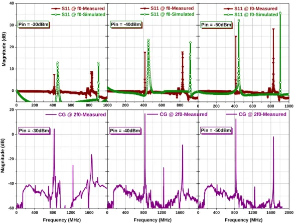
0 200 400 600 800 1000 0 10 20 30 40 200 400 600 800 0 200 400 600 800 1000 0 400 800 1200 1600 -60 -40 -20 0 20 0 400 800 1200 1600 0 400 800 1200 1600 2000 Magni tude (dB ) S11 @ f0-Measured S11 @ f0-Simulated Pin = -50dBm Pin = -50dBm Pin = -40dBm Pin = -30dBm Pin = -40dBm S11 @ f0-Measured S11 @ f0-Simulated S11 @ f0-Measured S11 @ f0-Simulated Magni tude (dB ) Frequency (MHz) CG @ 2f0-Measured Pin = -30dBm Frequency (MHz) CG @ 2f0-Measured Frequency (MHz) CG @ 2f0-Measured (a) (b) (c)
Fig. 15. Simulated (green) and measured (brown) reflection gain at fundamental frequency and measured conversion gain (purple) at the second harmonic frequency for the incident power (Pin) of (a) -30 dBm, (b) -40 dBm, and (c) -50 dBm. In the conversion gain graph, the frequency in x-axis is the frequency of the output signal
IEEE TRANSACTIONS OF MICROWAVE THEORY AND TECHNIQUES 9 TABLE IV:DESCRIPTION OF VARIOUS LINK BUDGET COMPONENTS
Link Budget component Term. Value
Forw ard
Power transmit by reader PT 15dBm
Reader antenna gain GR 4dBi
Free space loss @ 414.6 MHz = -27.55+20log(MHz)+20log(metre)
Power incident at tag (Pinc)= PT + GR - [email protected] Reve rse (Tag to read er)
Tag antenna gain GT 2dBi
Miscellaneous Loss at tag LT 1dB
Modulation Loss Pmod 6dB
Case I: Reflection gain provided by the HRA @ 414.6 MHz
Case II: Conversion gain provided by the HRA @ 829.2 MHz [email protected] [email protected] MHz> 414 MHz Fig. 13 (green) Fig. 13 (blue) Case I: Free Path loss @ 414.6 MHz
Case I: Free Path loss @ 829.2 MHz
[email protected] [email protected]
Case I: Power back to reader (Pread) @ 414.6 MHz
Pread = Pinc + GT - LT -Pmod - [email protected] + [email protected](RG)
Case II: Power back to reader (Pread) @ 829.2 MHz
Pread = Pinc + GT - LT -Pmod - [email protected] + [email protected]>414.6MHz(CG)
Initial Power PT=15dBm
Reader Antenna Gain GR=4dBi
HRA Tag Tag Antenna Gain
GT=2dBi
Miscellaneous loss (LT)= 1dB
Reader
Free Path Loss
[email protected] Reflection Gain [email protected] Modulation Loss Pmod=6dB Initial Power PT=15dBm
Reader Antenna Gain GR=4dBi
HRA Tag Tag Antenna Gain
GT=2dBi
Reader
Free Path Loss
Conversion Gain
[email protected]>414.6MHz
Free Path Loss
[email protected] Modulation Loss Pmod=6dB (a) (b) Case I Case II Miscellaneous loss (LT)= 1dB
Fig. 17. Complete system for calculating the power link budget in the forward and reverse path (a) Case I: reader transmits f0 (414.6 MHz) and tag re-radiates f0 (414.6 MHz), where tag provides reflection gain (b) Case II: reader transmits f0 (414.6 MHz) and tag re-radiates 2f0 (829.2 MHz), where tag provides conversion gain. Transmit Power Reflection Gain Conversion Gain
Noise Floor
Reader Tag Reader Tag
Tx Path loss @f0 Rx Path loss @2f0 Tx Path loss @f0 Rx Path loss @f0 0 25 50 75 100 125 150 -120 -100 -80 -60 -40 -20 0 20 25 50 75 100 125 150 Po wer (dBm) Reader-Tag Distance (a) (b)
Fig. 18. Forward and backward link budget for active RFID communication system (a) corresponds to Fig. 17 (a), (b) corresponds to Fig. 17 (b).
Above equation (7) is used to calculate the maximum read range of complete system, which also depends on the readers receive sensitivity. The reader sensitivity is good enough so that the signal reflected by the tag must be successfully detected by the reader. For the proposed link budget, we assume readers receive sensitivity is around -90 dBm. The maximum theoretical read range of active HRA is around 150m and 35m, which is shown in Fig 18 (a) and Fig. 18(b), corresponding to Case I (Fig. 17 (a)) and case II (Fig. 17 (b)), respectively.
IV. HARMONIC TUNNELING TAG DYNAMIC MODULATION The inherent negative resistance of tunnel diode enables HRA to be employed as a high gain modulator in backscattered low powered RFID systems. We introduced dual-band reflection amplifier in the previous section, it can modulate the backscatter signal by ON-OFF keying (OOK). It is more spectrally efficient than Frequency Shift Keying, as no energy is spent on the transmission of zero, but it is more prone to noise and interferences [60], [61].
In the proposed HRA, both the frequency bands are either ON or OFF simultaneously, leading to a compatibility with legacy system that do not operate using harmonic backscatter communication. The response of the HRA to the arbitrary waveform 0101101011101100 OOK modulation is shown in Fig. 19 with an incident wave power of -50dBm. It can be seen that the reflected power at fundamental frequency alternates between 0 dBm and 28 dBm, which leads to a more than 25 dB contrast between the ON-OFF states. Moreover, the wave generated from the fundamental at the second harmonic alternates at -20 dBm and 10 dBm, which means that even higher contrast is obtained. More contrast means the signal offers higher immunity to noise and interfering signals.
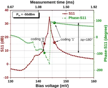
-10 0 10 20 30 0 10 20 30 40 50 -30 -20 -10 0 10 20 S11@f0 Ma gn itu de (d B) Time (ms) CG@2f0
Fig. 19. Relative output power (reflection gain) corresponding to an arbitrary bit sequence OOK modulation at f0=414.6 MHz, the ‘0’ state corresponds to circuit impedance Z= 5.6-j×0.2 Ω, whereas the ‘1’ state corresponds to Z= – 51.6-j×3.2 Ω (upper graph) and relative output power at 2f0= 829.2 MHz (conversion gain) where the ‘1’ corresponds to the input power at the fundamental being converted to the second harmonic frequency (lower graph). The ‘0’ state corresponds to no bias voltage, whereas the ‘1’ state corresponds to 144 mV.
Fig. 20. Capability of the HRA to perform BPSK by maintaining the magnitude symmetry of 16.8 dB, but with a phase difference of 180°, at two different biasing points Vb1= 142 mV (T1=1.262 ms) and Vb2= 146 mV (T2=1.277 ms),
respectively.
Phase Shift Keying (PSK) modulation can also be considered allowing constant power to be transferred to the transponder regardless of modulation state [62]. More specifically, BPSK is guaranteed with this circuit, as two phases responses are obtained for the same gain. The phase of the backscatter signal and reflection gain at f0 for the incident power of -50dBm is
shown in Fig. 20.
For Fig. 20, since the VNA could not control the dc bias, indirect measurement was performed. The bias generator was set to bias the HRA with slow ramp function from 0 to 300 mV, while VNA measurements have been done in time domain (thus on exact time corresponds to an exact bias). It is shown that a gain of 16.8 dB can be obtained for two different bias (ϕ=-97° when Vb =142 mV and ϕ=83°, when Vb =146 mV).
The phase stability as a function of the incident power is also measured to evaluate the impact of backscattering resilience to channel variation (Fig. 21). It is seen that the phase is quite stable at both frequencies.
-80 -70 -60 -50 -40 -30 -175 -150 -125 -100 -75 -50 Phas e ( de gree s) Incident Power (dBm) S11 @ f0>414.6 MHz S11 @ 2f0>829.2 MHz
Fig 21. Measured phase of the HRA at both frequency bands, f0 =414.6 MHz (wine) and at 2f0 =829.2 MHz (green) for various incident power, when optimum bias of 144 mV is applied.
V. CONCLUSION
This work describes the design and testing of a harmonic reflection amplifier using a tunnel diode that can amplify, backscatter and modulate the incident RF power in legacy RFID applications. It also operates in dual-band for transmitting information using the inherently generated 2nd harmonic. Its
ability to operate in dual-band improves the sensitivity of a communication link by avoiding the self-jamming leakage and also acts smartly in a crowded frequency spectrum. The demonstrated HRA is ideally suited for RFID applications that deserve high data rates with improved read range. The conversion gain as high as +18 dB at the 2nd harmonic opens the
way to integrate the proposed tunneling tag with inter-band mobile communication. The low power consumption and considerable reflection/conversion gains make the proposed HRA an idyllic candidate for RFID and inter-band 5G communication.
REFERENCES
[1] Red Pixie - The World of Data infographic Black and Blue.
[2] X. Gu, S. Hemour, and K. Wu, “Reconfigurable nonlinear circuit for wireless power harvesting and backscattering,” European Microw. Conf., Paris, France, Oct. 2019.
[3] A. Ramos, A. Lazaro and D. Girbau, "Semi-Passive Time-Domain UWB RFID System," IEEE Trans. Microw. Theory Techn., vol. 61, no. 4, pp. 1700-1708, April 2013
[4] A. Boaventura, J. Santos, A. Oliveira, and N. B. Carvalho, “Perfect isolation: Dealing with self-jamming in passive RFID systems,” IEEE Microw. Mag., vol. 17, no. 11, pp. 20–39, Nov. 2016.
[5] W-K. Kim, M-Q. Lee, J-S. Kim, H-S. Lim, J-W. Yu, B-J. Jang and J-S. Park, “A passive circulator with high isolation using a directional coupler for RFID,” IEEE MTT-S Int. Microw. Symp. Dig., 2006, pp. 1177–1180. [6] N.-C. Kuo, B. Zhao, and A. Niknejad, “Near-field power transfer and
backscattering communication to miniature RFID tag in 65 nm CMOS technology,” IEEE MTT-S Int. Microw. Symp. Dig., Jun. 2016, pp. 1–4. [7] A. Safarian, A. Shameli, A. Rofougaran, M. Rofougaran, and F.D.
Flaviis, “RF identification (RFID) reader front ends with active blocker rejection,” IEEE Trans. Microw. Theory Techn., vol. 57, no. 5, pp. 1320– 1329, May 2009.
[8] J.-Y. Jung, C.-W. Park, and K.-W. Yeom, “A novel carrier leakage suppression front-end for UHF RFID reader,” IEEE Trans. Microw. Theory Techn., vol. 60, no. 5, pp. 1468–1477, May 2012.
[9] S. Jung, M. Kim, and Y. Yang, “A reconfigurable carrier leakage canceler for UHF RFID reader front-ends,” IEEE Trans. Circuits Syst. I, Reg. Papers, vol. 58, no. 1, pp. 70–76, Jan. 2011.
[10] H. L. Lee, D.-H. Park, J.-W. Yu, and M.-Q. Lee, “Compact antenna module with optimized TX-to-RX isolation for monostatic RFID,” IEEE Microw. Wireless Compon. Lett., vol. 27, no. 12, pp. 1161–1163, Dec. 2017.
[11] M. Forouzandeh and N. Karmakar, “Self-interference cancelation in frequency-domain chipless RFID readers,” IEEE Trans. Microw. Theory Techn., vol. 67, no. 5, pp. 1994–2009, May 2019.
[12] M. Forouzandeh and N. Karmakar, “Application of wideband differential phase shifters with wide phase range in chipless RFID readers,” IEEE Trans. Microw. Theory Techn., vol. 67, no. 9, pp. 3636-3650, Sep. 2019 [13] M. Sajid and S. Chiu, “Canceling self-jammer and interfering signals in
an RFID system,” Aug. 16 2011, US Patent 8,000,674.
[14] R. Rimini, P. D. Heidmann, and J. P. Burke, “Method and apparatus for adaptive non-linear self-jamming interference cancellation,” Jun. 3 2014, US Patent 8,744,377.
[15] Y. Ma and E. C. Kan, “Accurate indoor ranging by broadband harmonic generation in passive NLTL backscatter tags,” IEEE Trans. Microw. Theory Tech., vol. 62, no. 5, pp. 1249-1261, May 2014.
[16] Y. Ma, X. Hui, and E. C. Kan, “Harmonic-wisp: A passive broadband harmonic RFID platform,” IEEE MTT-S Int. Microw. Symp. Dig. Jun. 2016, pp. 1–4.
[17] F. Amato and S. Hemour, “The harmonic tunneling tag: a dual band approach to backscattering communication,” IEEE Int. Conf. RFID
130 140 150 160 0.67 1.08 1.50 1.92 -10 0 10 20 30 40 coding '0' Pin = -50dBm Measurement time (ms) S11 Phase-S11 Bias voltage (mV) S11 (dB) coding '1' =180° -200 -100 0 100 Ph ase -S11 (de gree)
IEEE TRANSACTIONS OF MICROWAVE THEORY AND TECHNIQUES 11 Technol. Application, Pisa, Italy Sep. 2019.
[18] X. Gu, L. Guo, S. Hemour, and K. Wu, “Analysis and exploitation of diplexer-based fully passive harmonic transponder for 5G applications,” IEEE MTT-S Int. Microw. Symp. Dig., Dublin, Ireland, 2018.
[19] X. Gu, L. Guo, S. Hemour, and K. Wu, "Diplexer-Based Fully Passive Harmonic Transponder for Sub-6-GHz 5GCompatible IoT Applications," IEEE Trans. Microw. Theory Techn, vol. 67, no. 5, pp. 1675-1687, 2018. [20] X. Gu, L. Guo, S. Hemour, and K. Wu, "Novel diplexer-based harmonic transponder for 5G-compatible IoT applications," IEEE Wireless Power Transfer Conf. (WPTC), pp. 1-4, 2018.
[21] S. Khaledian, F. Farzami, B. Smida, and D. Erricolo, “Two-way backscatter communication tag using a reflection amplifier,” IEEE Microw. Wireless Compon. Lett., vol. 29, no. 6, pp. 421-423, Jun. 2019. [22] F. Amato, C. W. Peterson, B.P. Degnan, and Gregory D. Durgin,
“Tunneling RFID tags for long-range and low-power microwave applications,” IEEE J. Radio Freq. Identif., vol. 2, no. 2, pp. 93-103, Jun. 2018.
[23] F. Amato, H. M. Torun, and G.D. Durgin, “RFID backscattering in long range scenarios,” IEEE Trans. Wireless Commun., vol. 17, no. 4, pp. 2718-2725, Apr. 2018.
[24] F. Farzami, S. Khaledian, B. Smida, and D. Erricolo, “Reconfigurable dual-band bidirectional reflection amplifier with applications in van atta array,” IEEE Trans. Microw. Theory Techn., vol. 65, no. 11, pp. 4198-4207, Nov. 2017.
[25] F. Farzami, S. Khaledian, B. Smida, and D. Erricolo, “Ultra-low power reflection amplifier using tunnel diode for RFID applications,” IEEE Int. Symp. Antennas Propag., pp. 2511–2512 Jul. 2017.
[26] S. Khaledian, F. Farzami, D. Erricolo, and B. Smida, “A full-duplex bidirectional amplifier with low dc power consumption using tunnel diodes,” IEEE Microw. Wireless Compon. Lett., vol. 27, no. 12, pp. 1125– 1127, Dec 2017.
[27] J. Lee, and K. Yang, “RF power analysis on 5.8GHz low-power amplifier using resonant tunneling diodes” IEEE Microw. Wireless Compon. Lett., vol. 27, no. 1, pp. 61-63, Jan. 2017.
[28] F. Amato, C. W. Peterson, B. P. Degnan, and G. D. Durgin, “A 45 uw bias power, 34 dB gain reflection amplifier exploiting the tunneling effect for RFID applications,” IEEE Int. Conf. on RFID, pp. 137–144, Apr. 2015. [29] J. Kimionis, A. Georgiadis, M. Tentzeris, and A. Collado, “Enhancement
of RF tag backscatter efficiency with low-power reflection amplifiers,” IEEE Trans. Microw. Theory Techn., vol. 62, no. 12, pp. 3562-3571, Dec. 2014.
[30] J. Kimionis, M. Tentzeris A. Georgiadis, and A. Collado, “Inkjet-printed reflection amplifier for increased-range backscatter radio,” IEEE Eur. Microw. Conf. (EuMC), Oct. 2014.
[31] J. Kimionis, A. Georgiadis, S. Kim, A. Collado, K. Niotaki, and M. Tentzeris, “An enhanced-range RFID tag using an ambient energy powered reflection amplifier,” IEEE MTT-S Int. Microw. Symp. (IMS), June 2014, pp. 1–4.
[32] J. Lee, J. Lee, and K. Yang, “Reflection-type RTD low-power amplifier with deep sub-mW dc power consumption” IEEE Microw. Wireless Compon. Lett., vol. 24, no. 8, pp. 551-553, Aug. 2014.
[33] P. Chan and V. Fusco, “Full duplex reflection amplifier tag,” IET Microw., Antennas Propag., vol. 7, no. 6, pp. 415–420, Apr. 2013. [34] A. Lazaro, A. Ramos, R. Villarino, and D. Girbau, “Time-domain UWB
RFID tag based on reflection amplifier,” IEEE Antennas and Wireless Propag. Lett., vol. 12, pp. 520–523, 2013.
[35] V. Vesterinen, J. Hassel, and H. Seppa, “Tunable impedance matching for josephson junction reflection amplifier,” IEEE Trans. Appl. Supercond., vol. 23, no. 3, June 2013.
[36] J.-F. Bousquet, S. Magierowski, and G. Messier, “A 4-GHz active scatterer in 130-nm CMOS for phase sweep amplify-and-forward,” IEEE Trans. Circuits and Systems I: Regular Papers, vol. 59, no. 3, pp. 529– 540, March 2012.
[37] P. Chan and V. Fusco, “Bi-static 5.8 GHz RFID range enhancement using retrodirective techniques,” IEEE Eur. Microw. Conf. (EuMC), Oct 2011, pp. 976–979.
[38] H. Cantu, V. Fusco, and S. Simms, “Microwave reflection amplifier for detection and tagging applications,” IET Microw., Antennas Propag., vol. 2, no. 2, pp. 115–119, Mar. 2008.
[39] H. Cantu and V. Fusco, “A 21 GHz reflection amplifier MMIC for retrodirective antenna and RFID applications,” Inst. of Engineering and Tech. Seminar MM-Wave Products Tech., pp. 66–70, Nov. 2006. [40] S. Chung, S. Chen, and Y. Lee, “A novel bi-directional amplifier with
applications in active Van Atta retrodirective arrays,” IEEE Trans. Microw. Theory Tech., vol. 51, no. 2, pp. 542-547, Feb. 2003.
[41] Y. Ma and E.C. Kan, “Accurate indoor ranging by broadband harmonic generation in passive NLTL backscatter tags,” IEEE Trans. Microw. Theory Techn., vol. 65, no. 15, pp. 1249-1261, May. 2014.
[42] Lin , J. Bito, J.G. D. Hester, J. Kimionis, R.A. Bahr, and M.M. Tentzeris, “On-Body Long-Range Wireless Backscattering sensing system using inkjet-/3-d-printed flexible ambient RF energy harvesters capable of simultaneous dc and harmonics generation,” IEEE Trans. Microw. Theory Techn., vol. 65, no. 1, pp. 5389-5400, Dec. 2017.
[43] X. Chen, Y. Chen, H. Zhang, N. Yan, J. Wang, H. Min, and L-R. Zheng, “Long read range class-3 uhf rfid system based on harmonic backscattering,” Electron. Lett., vol. 54, no. 22, pp. 1262-1264, Nov. 2018.
[44] V. Palazzi, F. Alimenti, P. Mezzanotte, G. Orecchini, and L. Roselli, “Zero-power, long-range, ultra low-cost harmonic wireless sensors for massively distributed monitoring of cracked walls,” in IEEE MTT-S Int. Microw. Symp. Dig., Honolulu, HI, USA, Jun. 2017, pp. 1335–1338. [45] K. Rasilainen, J. Ilvonen, A. Lehtovuori, J.-M. Hannula, and V. Viikari,
“On design and evaluation of harmonic transponders,” IEEE Trans. Antennas Propag., vol. 63, no. 1, pp. 15–23, Jan. 2015.
[46] A. Lazaro, R. Villarino, and D. Girbau, “A passive harmonic tag for humidity sensing,” Int. J. Antennas Propag., vol. 2014, Jul. 2014, http://dx.doi.org/10.1155/2014/670345.
[47] K. Gumber, F. Amato, C. Dejous, and S. Hemour, “Nonlinear negative resistance-based harmonic backscatter,” IEEE MTT-S Int. Microw. Symp. Dig., Los Angeles, USA, Aug. 2020.
[48] S. Hemour, Y. Zhao, CHP Lorenz, D. Houssameddine, Y. Gui, C-M. Hu, and K. Wu, “Towards low power high efficiency RF and microwave energy harvesting,” IEEE Trans. Microw. Theory Techn., vol. 62, no. 4, pp. 965-976, Apr. 2014.
[49] CHP Lorenz, S. Hemour, W. Li, Y. Xie, J. Gauthier, P. Fay, and K. Wu, “Breaking the efficiency barrier for ambient microwave power harvesting with heterojunction backward tunnel diodes,” IEEE Trans. Microw. Theory Techn., vol. 63, no. 12, pp. 4544-4555, Dec. 2015.
[50] A. A-Khalidi, K. H. Alharbi, J. Wang, R. Morariu, L. Wang, A. Khalid, J. Figueiredo, and E. Wasige, “Resonant tunneling diode terahertz sources with up to 1mW output power in the J-band,” IEEE Trans. THz Sci. Technol., vol. 10, no. 2, pp. 150–157, Mar. 2020.
[51] R. J. Hwu, A. Djuandi, and S. C. Lee, “Negative differential resistance frequency conversion with gain,” IEEE Trans. Microw. Theory Tech., vol. 41, no. 5, pp. 890-893, May 1993.
[52] F. S. Barner, and G. F. Eiber, “An ideal harmonic generator,” Proc. IEEE, vol. 53, pp. 693-695, Jul. 1965
[53] Y. Zhao, S. Hemour, T. Liu, and K. Wu, “Negative resistance based electronic impedance tuner,” IEEE Microw. Wireless Compon. Lett., vol. 28, no. 2, pp. 144-146, Feb. 2018.
[54] C. C. Hoffins and K. Ishii, “Conditions of oscillation for waveguide mounted tunnel diodes,” IEEE Trans. Microw. Theory Techn., vol. 12, no. 2, pp. 176–183, Mar. 1964.
[55] C. Kidner, I. Mehdi, J. R. East, and G. I. Haddad, “Power and stability limitations of resonant tunneling diodes,” IEEE Trans. Microw. Theory Techn., vol. 38, no. 7, pp. 864-872, Jul. 1990.
[56] C.E. Saavedra, B.R. Jackson, and S.S.K. Ho, “Self-oscillating mixers: a natural fit for active antennas,” IEEE Microw. Mag., vol. 14, no. 6, pp. 40–49, Sep. 2013.
[57] J. Zhang, Y. Wang, and Z. Chen, “Integration of a self-oscillating mixer and an active-antenna,” IEEE Microw. Guided Wave Lett, vol. 9, no. 3, pp. 117-119, Mar. 1999.
[58] C. Toker, “Self-oscillating tunnel diode mixer having conversion gain,” IEEE Trans. Microw. Theory Techn., vol. 20, no. 9, pp. 616-618, Sep. 1972.
[59] A. Lazaro, D. Girbau, and D. Salinas, “Radio link budgets for UHF RFID on multipath environments,” IEEE Trans. Antennas Propag., vol. 57, no. 4, pp. 1241-1251, Apr. 2009.
[60] J. Lee, J. Lee, and K. Yang, “An on-off mode RTD oscillator operating at extremely low power consumption,” IEEE Trans. Nanotechnol., vol. 11, no. 5, pp. 863-865, Sep. 2012.
[61] J. Wang, A. A-Khalidi, L. Wang, R. Morariu, A. Ofiare, and E. Wasige, “5-Gb/s 50-cm wireless link using a high power compact III-V 50-GHz transmitter,” IEEE Trans. Microw. Theory Techn., vol. 66, no. 11, pp. 4698-4705, Nov. 2018.
[62] S. Khaledian, F. Farzami, B. Smida, and D. Erricolo, “A power efficient implementation of in-band full-duplex communication system (ReflectFX),” Int. Symp. Signal Image Video and commun., Tunis, Tunisia, Nov. 2016 pp. 242-246.
Karan Gumber (Member, IEEE) was
born in Punjab, India in 1988. He received the M.E degree in electronics and communication from the University Institute of Engineering and Technology, Panjab University, Chandigarh, India, in 2012, and the Ph.D. degree in electronics and communication from the Indian Institute of Technology Roorkee, Uttarakhand, India in 2019. He is currently a Postdoctoral Fellow at the IMS Research Center, University of Bordeaux, France. His research has been concerned with Resonant tunneling diodes, backscattering, RFID, linearization techniques for high power amplifiers, software defined radios.
Corinne Dejous (M’13) received the
electronics engineer degree from the French “Grande École” ENSEIRB in 1991 (M.S. degree), and the Ph.D. degree in electronics from the University of Bordeaux, France, in 1994.
In 1996, she has been appointed Assistant Professor at the University of Bordeaux, and promoted in 2009 to Full Professor at ENSEIRB-MATMECA / Bordeaux INP, France, where she teaches electronic systems and instrumentation, chemical sensors and microsystems. She leads research at IMS laboratory (CNRS UMR 5218) in acoustic wave (bio)chemical microsensors and more generally wave-based resonant sensors, her research activities also include wireless microdevices. Major fields of applications aim health and environment purposes. She has been the head of the research group Ondes (Waves, formerly Microsystems) from 2011 to 2018. From 2016, she is in charge of the IMS Labs’ transverse topic « Environments ».
She co-authored over 80 publications in international journals or book chapters, 180 communications, she delivered many invited talks, and co-supervised 35 research projects. She is also involved in the French Chapter of the IEEE Sensors Council.
Simon Hemour (S’08–M’11–SM’16)
received the B.S. degree in electrical engineering from the University of Grenoble Alpes, Grenoble, France, in 2004, and the M.S. and Ph.D. degrees in optics, optoelectronics, and microwave engineering from the Grenoble Institute of Technology, Grenoble, France, in 2006 and 2010, respectively. In 2003, he was with the European Organization for Nuclear Research, Geneva, Switzerland, as a member of the Instrumentation Department, where he was involved in ATLAS experiment on the Large Hadron Collider. From 2006 to 2007, he was a Research Assistant with the Pidstryhach Institute of Applied Problems of Mechanics and Mathematics, National Academy of Science of Ukraine, Lviv, Ukraine. In 2007, he joined the IMEP-LAHC MINATEC Laboratory, Grenoble, France. From 2011 to 2015, he was with the Poly-Grames Research Center, École Polytechnique de Montréal, Montréal, QC, Canada, where he was coordinating
the Wireless Power Transmission and Harvesting Research Group. He joined the Université de Bordeaux, Bordeaux, France, in 2015, where he is currently an Associate Professor, and he leads research in wireless micro energy solutions for IoT and biomedical applications. His current research interests include wireless power transfer and hybrid energy harvesting, backscattering, nonlinear & negative resistance devices, innovative RF measurements, RF interferometry, low power microwave, and millimetre wave conversion circuits, development of RF transponders and sensors for wireless systems and biomedical applications.
Dr. Hemour is a member of the IEEE MTT-25 Wireless Energy Transfer and Conversion Technical Committee and of the IEEE MTT-28 Biological effect and medical application Technical Committee. He has been invited to give many invited talks and plenary speeches at various international meetings, conferences and forums, and his pioneering work on low power RF energy harvesting has been highly cited. He was the TPC chair of the 2018 Wireless Power Transfer Conference (WPTC), and will be the general chair of the 2022 WPTC. He is part of the Editorial Board of the Wireless Power Transfer journal (Cambridge University press), and he has served as guest editor for IEEE Transactions on Microwave Theory and Techniques, as well as for the IEEE Journal of Electromagnetics, RF and Microwaves in Medicine and Biology