HAL Id: hal-00257396
https://hal.archives-ouvertes.fr/hal-00257396
Preprint submitted on 19 Feb 2008HAL is a multi-disciplinary open access archive for the deposit and dissemination of sci-entific research documents, whether they are pub-lished or not. The documents may come from teaching and research institutions in France or
L’archive ouverte pluridisciplinaire HAL, est destinée au dépôt et à la diffusion de documents scientifiques de niveau recherche, publiés ou non, émanant des établissements d’enseignement et de recherche français ou étrangers, des laboratoires
Gold nanoparticle-pentacene memory-transistors
Christophe Novembre, David Guerin, Kamal Lmimouni, Christian Gamrat,
Dominique Vuillaume
To cite this version:
Christophe Novembre, David Guerin, Kamal Lmimouni, Christian Gamrat, Dominique Vuillaume. Gold nanoparticle-pentacene memory-transistors. 2008. �hal-00257396�
Gold nanoparticle-pentacene memory-transistors
Christophe Novembre1,3, David Guérin2, Kamal Lmimouni2, Christian Gamrat1, and Dominique Vuillaume2, a
1) Commissariat à l’énergie atomique, CEA-Saclay, LIST/LCE (Advanced Computer Technologies & Architectures), Bat. 528, F-91191cedex, Gif-sur-Yvette, France. 2) Molecular Nanostructures & Devices group, Institute for Electronics, Microelectronics
and Nanotechnology, CNRS & University of Lille, BP60069, avenue Poincaré, F-59652cedex, Villeneuve d'Ascq, France.
3) Commissariat à l’énergie atomique, CEA-Grenoble, MINATEC, LETI/DIHS, avenue des martyrs, F-38019cedex, Grenoble, France.
PACS: 85.30.Tv; 85.65.+h; 73.61.Ph; 81.07.Pr
We demonstrate an organic memory-transistor device based on a pentacene-gold
nanoparticles active layer. Gold (Au) nanoparticles are immobilized on the gate dielectric (silicon dioxide) of a pentacene transistor by an amino-terminated self-assembled monolayer. Under the application of writing and erasing pulses on the gate, large threshold voltage shift (22 V) and on/off drain current ratio of ~3x10⁴ are obtained. The hole field-effect mobility of the transistor is similar in the on and off states (less than a factor 2). Charge retention times up to 4500 s are observed. The memory effect is mainly attributed to the Au nanoparticles.
Organic devices have gained a very great interest both for the understanding of their electronic properties and for applications in low-cost, large-area, and flexible electronics. Among them, organic memories are less studied than organic field-effect transistors (OFET) and organic light-emitting diodes (OLED). Memory devices made of metal nanoparticles (NP) embedded in organic materials have been demonstrated.1-8 These devices used a vertical structure where the active layer (an organic semiconductor including metal nanoparticles) is sandwiched between two metal electrodes. However, this approach suffers from possible drawbacks induced by the metal deposition on top of the active organic layer. For instance, it has been reported that the switching effects are due to the formation/breaking of metallic nano-filaments rather than induced by electrostatic effects due to charge/discharge of the NPs.5, 9, 10 Here, we report on a horizontal three-terminal structure (transistor) which is not sensitive to that drawback. We demonstrate both a memory and a transistor effects combined in the same device. We report on/off ratio of ~3x10⁴, large threshold voltage shift (22 V) and retention time of ~4500 s.
We used a bottom-gate, bottom source-drain contacts OFET configuration. The gate is a highly-doped (p+) silicon wafer covered by a thermally grown 200 nm-thick silicon dioxide (SiO2). Source and drain electrodes (Ti/Au 20 nm/200 nm) were
evaporated through a shadow mask. Transistor sizes are: channel length L=12µm and width W=113µm. These structures are used as is for a reference sample (sample A). For sample B, the surface was functionalized by an amino-terminated self-assembled monolayer (SAM) before the NP deposition.11-13 First, gold (Au) electrodes were functionalized by dipping in a 2-amino ethanethiol molecules solution in ethanol
(10mg/mL) during 5h. The sample was then rinsed 3 times with alcohol and subsequently dried in argon stream. Second, the SiO2 surface was functionalized by immersion in a
solution of (3-aminopropyl) trimethoxysilane (APTMS) molecules diluted in toluene at a concentration 1.25µL/mL and at 60°C during 4min.14 Excess, non-reacted, molecules were removed by rinse in toluene, and then in alcohol under sonication. This sample was subsequently dried under argon stream. Static water contact angle was 19°, a common value for hydrophilic NH2-terminated surfaces.14 Sample B was then dipped in an
aqueous solution of citrate-stabilized Au-NP (colloidal solution purchased from Sigma Aldrich, 20 ± 3 nm in diameter) overnight under argon atmosphere. The sample was then cleaned with deionized water and alcohol, and dried under argon stream. Finally, Au-NP were encapsulated by dipping in a solution of 1,8-octanedithiol in ethanol (10µL/mL) during 5h to help the formation of a network of NPs. The sample was subsequently rinsed in alcohol and dried in argon stream. On a second sample (sample C), Au-NPs were directly deposited onto the surface without any surface functionalization. A drop of Au-NP in aqueous solution was deposited on the substrate and the sample was left at room temperature overnight. The NP progressively deposited on the substrate as the solvent was evaporated. Sample C was cleaned in an isopropanol bath, and then in deionized water. It was subsequently dried in argon stream.
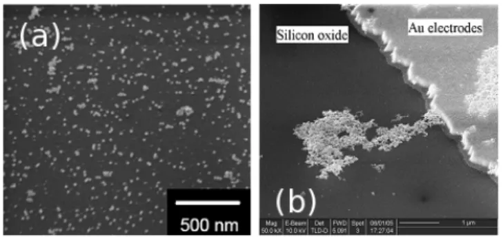
Scanning electron microscope (SEM) images, Fig. 1, show a random distribution of NPs for sample B, with the formation of some aggregates. From an image analysis, we deduce an average density of ~2-5x10¹⁰ NP/cm2. On the contrary, for sample C, we have only observed aggregates of NPs with no NP on the surface between them. An average density of 0.5-1.0x10¹⁰ NP/cm2 is roughly estimated (by dividing the area of the
aggregates by the known size of the NP and multiplying this number by the average number of aggregates per cm2). On the average, sample B has a higher NP density than sample C. This is expected since amino-terminated surfaces are know to react easily with Au-NP through electrostatic interactions between the negatively charged citrate overlayer of NPs and the protonated amino-terminated monolayer.13 These three samples (including the reference, sample A) were placed together in a vacuum evaporator to deposit a 50 nm-thick pentacene film a rate of 0.1 nm/s on a substrate kept at room temperature.
Electrical measurements were done in a glove-box (nitrogen purged) using an Agilent 4155C Semiconductor Parameter Analyzer. For each type of samples, we measured about 30 devices. To investigate the memory properties, we measured IDS-VGS
(at VDS= -20 V) and IDS-VDS (at VGS= -20 V) before and after writing and erasing pulses.
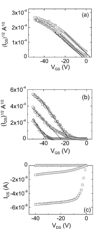
Writing pulse consisted in applying -50 V on the gate electrode during 20s, while the source and drain electrodes were grounded. To erase the memory, we applied +50V on the gate for the same time. Figure 2 presents typical results for the devices A and B. A clear effect is demonstrated with a large reduction of the drain current and shift of the threshold voltage after the writing pulse (Figs. 2-b and c). The maximum drain current on/off ratio is 2.6x10⁴ (at VGS = VDS = -20 V) and the maximum threshold voltage shift is
ΔVT ~ - 22 V. This on/off ratio is on a par with literature data reported for the vertical
two-terminals devices.1, 2, 4, 5 A similar effect (not shown), while lower in amplitude, is observed for device C: on/off ratio ~ 1.2x10² and ΔVT ~ - 3.5 V (see Table I). In these
two devices, these effects are larger than a very small one also observed in the reference device A (no Au-NP): on/off ~ 2.2 and ΔVT ~ - 2 V (Fig. 2-a). For a pentacene alone
in the pentacene films or at the gate dielectric/pentacene interface.15 It is clear that the presence of Au-NPs induces larger effects. We can also notice that after the write operation, the slope of (IDS)1/2-VGS characteristics does not changed too much (Fig. 2-b),
meaning that the influence of writing on charge carrier mobility is small (less than a factor ~ 2). The large negative ΔVT can be ascribed to the trapping of positive charges in
the Au-NP at the pentacene/dielectric interface. With an oxide capacitance Cox = 1.7x10⁻⁸
F.cm-2, about 2x10¹² charges per cm2 are stored in the Au-NPs, i.e. about 40-100 charges per NP for device B (calculated from the maximum ΔVT). The smaller ΔVT for device C
is consistent with the smaller NP density. An exact calculation of the charge density per NP is not very significant here due to the very crude estimate of this NP density for device C. However, we can notice that ΔVT in device C is smaller by a factor ~ 6 than in
device B, while the NP density is smaller by a factor 2-10. Given these rough estimates, these results seem consistent with almost the same order of magnitude of charges per NP in devices B and C (Table I). Moreover, some differences in ΔVT can also come from the
difference in the morphology of the NPs deposition (random network vs. large aggregates, see Fig. 1). After the erasing pulse at +50V/20s, the recovery is not complete. A complete recovery is obtained at larger bias or longer time. This asymmetry between the writing and erasing conditions can be explained by the fact that for VGS > 0 the
organic transistor is in depletion mode. Then, a space charge region appears in the semiconductor. A part of the potential drop is supported by the space charge region in the semiconductor, thus lowering the potential seen by nanoparticles at the pentacene/dielectric interface. These results show that the memory effect is due to the storage of holes in NPs. This is in agreement with charge storage properties recently
demonstrated by Leong et al.16 in a silicon/SiO2/APTES/NPs/pentacene/Au vertical
(capacitor-like) structure (APTES is 3-aminopropyl-triethoxysilane). In this last work, hysteresis has been observed in the capacitance-voltage characteristics, with a voltage shift of about 1-2 V achieved with writing/erasing voltages in 5-10V range. Taking into account the thinner oxide (4.5 nm in this latter case), the memory effect amplitude (~ 4-7x10¹² stored charges/cm2) is on a par with our results.
We also observed that the device B (before any writing) has a more negative VT
and a higher drain current than the reference device A (Figs. 2-a and b). The more negative VT may be related to the surface functionalization by the positively charged
amino-terminated SAM.17 This shift (~ - 6V compared to device A) corresponds to about 6x10¹¹ charges/cm2. A similar effect, also observed for device C (no SAM), may be due to a surface oxide contamination by the overnight exposition to the citrate-stabilized NP solution which also contains Na+ ions (which are well known as SiO2 contaminants).18
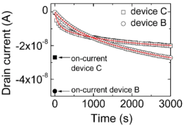
We investigated the charge retention properties of the memory, i.e. the relaxation dynamics of trapped charge carriers after writing of the device. This relaxation was measured by connecting all the three electrodes of the device to the ground, and regularly measuring (every 20s) the drain current at VDS = VGS = - 20 V during a limited time,
namely 2ms. We ensured that this measurement method induced limited charging effect, which can perturb the measurement of the charge relaxation, by checking on a non charged device. No significant charge effect has been detected for this measurement condition. Figure 3 shows the charge relaxation measured on devices B and C after writing at VDS = -50 V for 20 s.
We observed a slow recovery of the drain current. All the data can be fitted by the sum of two exponentials as shown by the red lines. The extracted time constants, with the dispersion limits, are given Table II. We have observed the same trends for devices C. Device A (no NP), exhibited a smaller amplitude of drain current variation and smaller time constants. We can also define a half-amplitude retention time as the time needed to reach a drain current ID(1/ 2)=ID(0)+ 12
[
ID( )! "ID(0)]
where ID(0) is the off current(at t=0 after the writing pulse) and ID(∞) is the on current (at a complete recovery). These
values are also summarized in Table II. Our best result (~ 4500 s, see Table II) is shorter than reported data for a vertical two-terminal memory device (~ 104-105 s).1, 6 We can notice that time constants and half-amplitude retention times are higher in device B than in device C. This is consistent with the fact that device B presents a higher NPs density, and as a consequence, more charge retention centers than device C. Note that time constants for device A are of the same order of magnitude than those reported by Gu et al. for a pentacene-based OFET.15 The physical origins of these two time constants remain unclear at the moment and deserve further studies.
In summary, we have demonstrated an organic memory combined with a transistor. The charge trapping and charge retention are attributed to the presence of a layer of Au-NPs at the pentacene/dielectric interface. A larger memory effect is observed when NPs are immobilized on the SiO2 gate dielectric through an amino-terminated
self-assembled monolayer, compared to NPs deposited on a naked SiO2 surface. This
“two-in-one” organic memory-OFET would be advantageously used in circuit design and integration for low-cost organic electronics. This may simplify memory-cell design since a charge retention capacitance is not required. Similarly, such a single device may be
used to drive an OLED instead of 2 to 4 OFET. Further works are in progress to study the writing/erasing times, the cycling stability, and to address the relationship between the memory performances, the size, organization and distribution of NPs.
The authors thank R. Baptist (CEA) for his support. This work was supported by the Micro and Nanotechnology Program from French Ministry of Research under the grant RTB: “Post CMOS moléculaire”.
1. L. Ma, J. Liu and Y. Yang, Appl. Phys. Lett. 80 (16), 2997 (2002).
2. L. Ma, S. Pyo, J. Ouyang, Q. Xu and Y. Yang, Appl. Phys. Lett. 82 (9), 1419 (2003).
3. A. Kiesow, J. E. Morris, C. Radehaus and A. Heilmann, J. Appl. Phys. 94 (10), 6988 (2003).
4. L. D. Bozano, B. W. Kean, V. R. Deline, J. R. Salem and J. C. Scott, Appl. Phys. Lett. 84 (4), 607 (2004).
5. D. Tondelier, K. Lmimouni, D. Vuillaume, C. Fery and G. Haas, Appl. Phys. Lett.
85 (23), 5763 (2004).
6. Y. Yang, J. Ouyang, L. Ma, R. J.-H. Tseng and C.-W. Chu, Adv. Func. Mater. 16, 1001 (2006).
7. J. C. Scott and L. D. Bozano, Adv. Mat. 19, 1452 (2007). 8. J. He, J. Wu and Y. Yang, J. Appl. Phys. 97, 064507 (2005).
9. M. Cölle, M. Büchel and D. M. De Leeuw, Org. Electron. 7, 305 (2006). 10. F. L. E. Jakobsson, X. Crispin, M. Cölle, M. Büchel, D. M. De Leeuw and M.
Berggren, Org. Electron. 8, 559 (2007).
11. H. X. He, D. Zhang, Q. G. Li, T. Zhu, S. F. Y. Li and Z. F. Liu, Langmuir 16 (8), 3846 (2000).
12. T. Sato, H. Ahmed, D. Brown and B. F. G. Johnson, J. Appl. Phys. 82 (2), 696 (1997).
14. D. F. Siqueira Petri, G. Wenz, P. Schunk and T. Schimmel, Langmuir 15 (13), 4520 (1999).
15. G. Gu, M. G. Kane, J. E. Doty and A. H. Firester, Appl. Phys. Lett. 87, 243512 (2005).
16. W. L. Leong, P. S. Lee, S. G. Mhaisalkar, T. P. Chen and A. Dodabalapur, Appl. Phys. Lett. 90, 042906 (2007).
17. S. Kobayashi, T. Nishikawa, T. Takenobu, S. Mori, T. Shimoda, T. Mitani, H. Shimotani, N. Yoshimoto, S. Ogawa and Y. Iwasa, Nature Materials 3, 317 (2004).
18. E. H. Nicollian and J. R. Brews, MOS (Metal Oxide Semiconductor) physics and
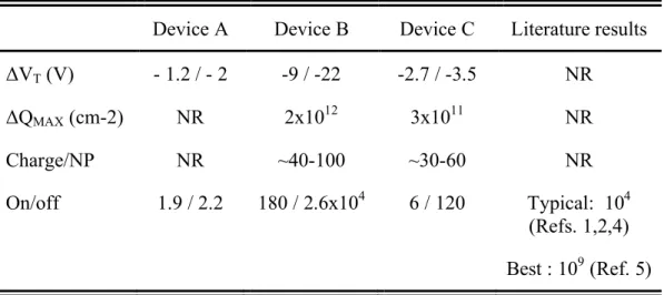
Table I. Threshold voltage shift, density of stored charges, stored charge per NP and on/off drain current ratios (NR stands for non-relevant). Min / max values are given, except for ΔQ and charges/NP, calculated from the maximum ΔVT.
Device A Device B Device C Literature results
ΔVT (V) - 1.2 / - 2 -9 / -22 -2.7 / -3.5 NR ΔQMAX (cm-2) NR 2x10¹² 3x10¹¹ NR Charge/NP NR ~40-100 ~30-60 NR On/off 1.9 / 2.2 180 / 2.6x10⁴ 6 / 120 Typical: 104 (Refs. 1,2,4) Best : 109 (Ref. 5)
Table II. Time constants and retention times measured on devices A, B and C. Min / max values are given (NR stands for non-relevant).
Device A Device B Device C Literature
results Time constant τ1 (s) 20 / 30 420 / 450 100 / 200 NR Time constant τ2 (s) 350 / 400 1500 / 3000 1500 / 2500 NR Half-amplitude retention time t1/2 (s) 140 / 270 1600 / 4530 635 / 1270 104 - 105 (Refs. 1,6)
Fig. 1 : (a) SEM images of sample B after deposition and encapsulation of Au-NP and (b) of sample C after deposition of nanoparticules. Deposition of nanoparticles on the extent of respective surfaces is similar to the presented images. On both images light areas represent 20nm Au nanoparticles, and the darker background is the oxide substrate.
FIG. 2. (IDS)1/2-VGS (at VDS = -20V) for (a) device A and (b) device B and (c) IDS-VDS
(at VGS = -20V) characteristics for device B before () and after () writing (at VGS
= -50V, 20s) and () erasing (at VGS = 50V, 20s) operations. Solid lines on the
FIG. 3. Charge relaxations in devices B and C after writing at VGS = -50V, 20s.
Open symbols are the initial on-current before writing. The full lines are fits with two exponentials.