HAL Id: hal-01979152
https://hal.archives-ouvertes.fr/hal-01979152
Submitted on 8 Jul 2019HAL is a multi-disciplinary open access archive for the deposit and dissemination of sci-entific research documents, whether they are pub-lished or not. The documents may come from teaching and research institutions in France or abroad, or from public or private research centers.
L’archive ouverte pluridisciplinaire HAL, est destinée au dépôt et à la diffusion de documents scientifiques de niveau recherche, publiés ou non, émanant des établissements d’enseignement et de recherche français ou étrangers, des laboratoires publics ou privés.
Atmospheric Pressure Spatial Atomic Layer Deposition
Afzal Khan, Viet Huong Nguyen, David Muñoz-Rojas, Sara Aghazadehchors,
Carmen Jimenez, Ngoc Duy Nguyen, Daniel Bellet
To cite this version:
Afzal Khan, Viet Huong Nguyen, David Muñoz-Rojas, Sara Aghazadehchors, Carmen Jimenez, et al.. Stability Enhancement of Silver Nanowire Networks with Conformal ZnO Coatings Deposited by Atmospheric Pressure Spatial Atomic Layer Deposition. ACS Applied Materials & Interfaces, Wash-ington, D.C. : American Chemical Society, 2018, 10 (22), pp.19208-19217. �10.1021/acsami.8b03079�. �hal-01979152�
Stability enhancement of silver nanowire networks
with conformal ZnO coatings deposited by
atmospheric pressure spatial atomic layer
deposition
Afzal Khan†, §, ‡, Viet Huong Nguyen†, ‖, ‡, David Muñoz-Rojas†,*, Sara Aghazadehchors†, ⸸,
Carmen Jiménez†, Ngoc Duy Nguyen ⸸, Daniel Bellet†
†Univ. Grenoble Alpes, CNRS, Grenoble INP, LMGP, F-38000 Grenoble, France.
§Department of Physics, Univ. of Peshawar, Pakistan.
ǁCEA-INES, LITEN, F-73375, 50 Avenue du Lac Léman, Le Bourget-du-Lac, France
⸸Département de Physique, Université de Liège, CESAM/Q-MAT, SPIN, B-4000 Liège,
Belgium.
‡ These authors contributed equally to this work
*Corresponding author: david.munoz-rojas@grenoble-inp.fr
Keywords: Transparent electrode, stability, conformal coating, ZnO, Spatial Atomic Layer
Abstract:
Silver nanowire (AgNW) networks offer excellent electrical and optical properties and have emerged as one of the most attractive alternatives to transparent conductive oxides to be used in flexible optoelectronic applications. However, AgNW networks still suffer from chemical, thermal and electrical instabilities which in some cases can hinder their efficient integration as transparent electrodes in devices such as solar cells, transparent heaters, touch screens or organic light emitting diodes (OLEDs). We have used atmospheric pressure spatial atomic layer deposition (AP-SALD) to fabricate hybrid transparent electrode materials in which the AgNW network is protected by a conformal thin zinc oxide layer. The choice of AP-SALD allows to maintain the low-cost and scalable processing of AgNW based transparent electrodes. The effects of the ZnO coating thickness on the physical properties of AgNW networks are presented. The composite electrodes show a drastic enhancement of both thermal and electrical stabilities. We found that bare AgNWs were stable only up to 300 °C when subjected to thermal ramps while the ZnO coating improved stability up to 500 °C. Similarly, ZnO coated AgNWs exhibited an increase of a 100 % in electrical stability with respect to bare networks, withstanding up to 18 V. A simple physical model shows that the origin of the stability improvement is the result of hindered silver atomic diffusion thanks to the presence of the thin oxide layer and the quality of the interfaces of hybrid electrodes. The effects of ZnO coating on both the network adhesion and optical transparency are also discussed. Finally, we show that the AP-SALD ZnO-coated AgNW networks can be effectively used as very stable transparent heaters.
Introduction
Transparent electrodes (TE) constitute a critical component within a wide range of devices including smart windows, touch screens, solar cells, organic light emitting diodes (OLED) or transparent heaters. Such electrodes need to be optically transparent and electrically conductive to a certain extent1,2 depending on the targeted application. While the main transparent conductive materials studied for several decades have been transparent conductive oxides (TCO), alternative emerging thin layers have been explored recently.3 Among them, metallic nanowire networks and specially those composed of silver nanowires (AgNW) have attracted much attention in the past few years.4–8 By virtue of their excellent electrical and optical properties (10-20 Ω/sq sheet resistance and about 90 % transmittance in the visible range)4,9 and their mechanical flexibility,7 silver nanowire networks are considered as promising candidates for flexible optoelectronic applications. Another clear advantage of AgNW based TE is the possibility to establish simple large-scale fabrication through solution processing10 and a lower price than indium tin oxide (ITO),11 which is so far considered as the most standard and efficient transparent conducting oxide.1 It has even been shown that by further optimizing the deposition and post-deposition conditions, and the aspect ratio (length/diameter) of the nanowires, the resulting networks can surpass the electro-optical properties of (ITO).9 AgNW networks have been investigated or even efficiently integrated into devices such as transparent heaters,12–15 solar cells,16–20 touch screens,21,22 electromagnetic shielding23 or antennas,24 OLEDs,25 in electrochromic devices,26 for medical purposes27 as well electrically conductive textiles28.
Despite the attracting potentialities described here above, the integration of AgNW based TE in real devices is not yet widely considered in industrial devices due namely to their potential thermal29 and electrical30 instabilities, as well as low adhesion7 and aging issues.31,32 For instance, while an electrical welding33 or thermal annealing29,34 is beneficial for reducing
junction resistance (between adjacent AgNWs) thanks to local sintering, it is also known that reaching too high a temperature leads to spheroidization of the AgNWs. This causes the loss of the percolating nature of the network, thus eventually leading to an infinite electrical resistance.29 Left unprotected, AgNW networks would undergo local oxidation and/or melt, which adversely affect the conductivity of AgNW films. While the melting point of bulk silver is above 960 °C, degradation induced by thermal annealing can occur at much lower temperature (i.e. < 300 °C) due to the high surface-to-volume ratio in nanowires.9
The idea of preparing composite electrodes by coating metallic nanowires with a very thin oxide layer has already been considered in literature19 as a possible remedy to such instabilities. Some researchers have used titanium dioxide (TiO2) coatings35–37, as well as
ZnO38–40 or aluminum doped zinc oxide (ZnO:Al).41 Clearly, the shell used has shown encouraging results in terms of stability enhancement. However, in order for such composite electrodes to remain attractive in terms of cost and simple processing, the oxide layer should be deposited by low-cost, vacuum-free scalable approaches. The methods so far reported (Atomic Layer Deposition (ALD), spin-coating or sputtering)35–39,41 can be associated to drawbacks such as the use of vacuum or the difficulty for upscaling, thus compromising the intrinsic low-cost and scalability of AgNW based TE. Atmospheric Pressure Spatial Atomic Layer Deposition (AP-SALD) is a promising recent approach to ALD that can operate at atmospheric pressure, is easily scalable and up to two orders of magnitude faster than ALD.
42 This is so thanks to the spatial separation of precursors in AP-SALD, which eliminates the
need for purges between successive precursor injections in conventional ALD.42–44 AP-SALD has already been used to deposit high-quality oxide films as passive and active components for new generation solar cells and other devices.42,45 The efficiency of AP-SALD films to protect transparent heaters based on Cu nanowires from chemical oxidation has also been shown recently.46
The present study focuses on the use of AP-SALD to deposit ZnO coatings on AgNWs based TE, and the thorough investigation of the effects of the ZnO coating thickness on the properties of AgNW networks in terms of electrical and thermal stabilities. We have used a home-made AP-SALD system to fabricate ZnO-AgNW composite electrodes. We demonstrate that AP-SALD is a suitable technique to deposit in a few minutes a conformal compact oxide layer of a controlled thickness (up to 30 nm), which drastically improves the thermal and electrical stability of the networks. We also introduce a simple model that allows to explain the stability enhancement provided by the ZnO coating. The effects of ZnO coating on both the network adhesion and optical transparency are also discussed. Finally, we show that the AP-SALD ZnO-coated AgNW networks can be effectively used as very stable transparent heaters.
Methods and experimental conditions
Deposition of AgNW networks:AgNW suspensions in isopropanol were purchased from Seashell technology, USA. The average length of AgNWs was 32 µm while their average diameter was 130 nm. The as-received suspensions, with initial concentration of 10 mg/ml, were diluted to various concentrations and then deposited on Corning glass (C1737-S111) substrates using spin coating at room temperature. The substrates were cleaned through a sonication in acetone, then rinsed in isopropanol, then washed with distilled water and finally dried with N2 gas before AgNW deposition. Deposition parameters (nanowires solution concentration, rotating speed of the spin coater and dispensing rate) and post-deposition thermal annealing parameters (temperature and duration) were optimized to obtain highly transparent (~90 % transmittance) and highly conductive (~10 Ω/sq sheet resistance) AgNW networks. The best electro-optical properties of AgNW networks were obtained by spin-coating 1 ml of
suspension (0.5 mg/ml, in two stages of 0.5 ml each with a 20 s pause between them, allowing the surface to dry) over 2.5 cm x 2.5 cm corning glass substrates at ambient atmospheric conditions using a spin-coater with rotation of 1500 rpm. The optimal post-deposition thermal annealing (250 °C for 30 minutes) step is necessary to desorb the organic residues and to decrease the electrical resistance of the junctions between adjacent AgNWs.29
A second set of samples was deposited for performing isothermal annealing tests and to test the electrical stability using different voltage ramps. In this case, the diameter of NWs was around 90 nm and the lengths could vary from 10 to 20 um. The initial suspension was diluted to 0.2g/L prior to deposition. An airbrush infinity CR was used to spay NWs on corning glass substrates. During deposition, a N2 flow at 3 bar was used, and the airbrush
scanned the substrate in the X-Y direction for 15 cycles. The substrates were kept at 90 °C during the deposition. The as-deposited samples were annealed at 230 °C for 1 h to minimize the electrical resistance and ensure intimate junction between adjacent AgNWs.
Deposition of ZnO coatings
The ZnO coatings were deposited using a home-made AP-SALD system previously reported.42,47,48 The deposition parameters were optimized and then ZnO growth was carried out at 200 °C, using diethylzinc ((C2H5)2Zn; DEZ) and water vapor as precursors for zinc and
oxygen, respectively. The samples were placed at a distance of 200 µm under the injection head oscillating at 10 cm/s. In our deposition head, there are two channels for the metal precursor. Thus, each sample oscillation (forth and back) corresponds to four ALD cycles.49 The system allows to deposit over an area of 5 cm x 5 cm.
Morphological and optical characterization
Optical characterization of the AgNW networks was performed with a Perkin Elmer Lambda 950 UV-Visible-Near IR spectrophotometer equipped with an integrating sphere, which allows measuring the total optical transmittance/reflection. Such measurements were performed in two different locations for each sample and then averaged.
Optical microscopy images of the AgNW networks were obtained with a Leica DM LM microscope. Scanning electron microscopy (SEM) and transmission electron microscopy (TEM) images were obtained using, respectively, a FEG-SEM Environmental FEI QUANTA 250 operating at an accelerating voltage of 10 keV and a JEOL JEM-2010 microscope operating at 200 keV. The sample preparation for TEM imaging was performed using the crushing technique.
Thermal and electrical stability studies
The stability of AgNW networks was assessed through in situ measurement of the network electrical resistance during either thermal or voltage ramps by using a two-probe setup with a Keithley 2400 sourcemeter. Thermal stability was studied by subjecting the AgNW networks to thermal ramps from room temperature to 500 oC at a rate of 2 oC/min. Isothermal test at 320 °C for 1 hour w also performed.
The electrical stability of the networks was measured in two ways. In the first constant voltage ramp at a rate of 0.1 volt/min, were applied up to specimen failure (i.e. when the electrical resistance diverged) to samples coated with different ZnO thicknesses (the networks used were fabricated using the AgNWs with an average diameter of 130 nm). In the second, equivalent networks made using the AgNWs with average diameter of 90 nm where coated with 25 nm of ZnO and different voltage ramps were applied, namely, 0.05, 0.075 and 0.1 volt/min.
To assess the use of these AgNW networks as transparent heater, different voltages were applied while the temperature of the samples was measured in situ using a thin resistance temperature detector (RTD) embedded in a 120 µm thick PET layer, therefore limiting thermal inertia. The RTD was placed in thermal contact with the sample, below the substrate (details on the setup have been reported previously.9,50
Results and Discussion
ZnO coating of AgNW network with AP-SALD and effect on adhesion and transparence
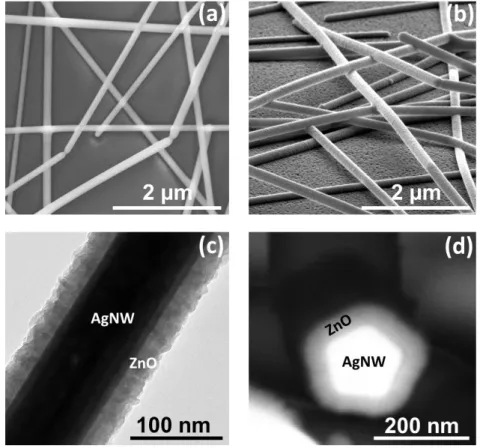
A SEM image of the bare AgNWs annealed at 250 oC for 30 minutes is shown in Figure 1a, where effective sintering of the wires at the junctions is clearly visible. A coated AgNW network with a 30 nm thick ZnO coating deposited with AP-SALD is shown in the SEM image in Figure 1b. The distinct morphology of the ZnO coating can be observed both on the nanowires and the glass surface. As shown in the figures, the surface of the bare nanowires appears smooth while that of ZnO-coated AgNWs show the typical granular morphology of ZnO coatings deposited by AP-SALD.47
Figure 1. (a) Scanning electron microscopy (SEM) image of the AgNW network deposited
by spin coating and annealed at 250 oC for 30 minutes to sinter the junctions, (b) SEM image of AgNW networks coated with 30 nm of ZnO (obtained with 60 sample oscillations). (c) Transmission electron microscopy (TEM) image of a 30 nm thick ZnO coated AgNW, (d) Back scattered SEM image of a coated AgNW (allowing to highlight the elemental contrast) showing the usual fivefold symmetry twinning of AgNWs surrounded by a uniform 30 nm thick ZnO layer.
A transmission electron microscopy (TEM) image of a 30 nm coating of ZnO on a AgNW is shown in Figure 1c. Such coating appears very conformal: this point is crucial since this is a prerequisite for an efficient protection against any instability. As in ALD, in AP-SALD the ZnO layer thickness is proportional to the number of AP-SALD cycles, i.e. sample oscillations under the head. The growth rate r was thus estimated from the thickness measured for the thicker ZnO layer deposited on AgNWs divided by the number of AP-SALD oscillations. As reported in Figure 1c, a ZnO thickness of 30 nm is observed for 60
AP-SALD cycles. The growth rate was thus ~ 0.50 nm/oscillation (as stated above, in our AP-SALD system a sample oscillation is equivalent to 4 conventional ALD cycles47, thus yielding a growth per cycle (GPC) of about 1.25 Å/ALD cycle). Figure 1d shows a back scattered SEM image of a ZnO coated AgNW which enables to highlight the elemental contrast: the usual fivefold symmetry twinning of AgNWs7 is well seen, as well as the surrounding uniform ZnO layer. Again the conformal and continuous aspect of the coating appears in a very clear way in this image.
Before focusing on the effects of ZnO coating on electrical and thermal stability of AgNW networks, we first consider the effects on both the network adhesion and optical transparency.
It is known that low adhesion of AgNW networks to the substrate can be one of the drawbacks of these materials when used as TE7: even a gentle rub can remove nanowires from the substrate. The influence of the AP-SALD ZnO coating on the adherence of AgNW network on the glass substrate was thus investigated. To do so a scotch tape test was applied to both the bare and the coated networks to qualitatively compare their adhesion strength to the substrates. Figure 2a and 2b show the optical microscope images of the bare and the ZnO coated AgNWs networks at the edge of the locations where the tape was applied. The upper parts in the figures correspond to the areas in which the scotch tape test was applied, while the lower parts correspond to areas outside the tested zone. Figure 2a corresponds to the bare AgNWs, while Figure 2b corresponds to the ZnO coated AgNWs. It can be clearly seen from Figure 2a that for bare AgNW networks most of the nanowires are removed, showing the very low adhesion of the bare AgNWs to the substrate. Conversely, Figure 2b shows that for coated networks numerous nanowires remained on the substrate, thereby showing a clear improvement in AgNWs adhesion to the substrate. The low resistance of the networks was also maintained after the tape test, while for uncoated networks the resistance after the tape test was 3 orders of magnitude higher (k).
Figure 2. (a-b) Optical microscope images of the bare and coated (30 nm) AgNW network,
respectively, showing the effect of the scotch tape test. The upper (lower) half is the region where tape was (not) applied; (c) Transmittance of AgNW networks at 550 nm (after subtraction of the glass substrate transmittance) versus the ZnO coating thickness deposited by AP-SALD. Increase in thickness of the ZnO coating results in a linear decrease of the transmittance.
The effect of the ZnO coating on electrode transparency was also evaluated. Figure 2c reports the influence of the ZnO coating thickness on the optical transparency (measured for a wavelength of 550 nm) of coated AgNW networks. Note the network transmittance is measured after subtracting the substrate contribution, as explained in Lagrange’s et al. article.9 In a first approximation a linear decrease of optical transparency from 93.5 % to 82.5 % can be observed (as expected for a linear expansion of an exponential function close to unity). For an optimized integration of coated AgNW network a compromise should be considered, depending on the application targeted. Indeed, as seen below, a thicker ZnO coating is associated to a more efficient thermal and electrical stability but at the expenses of optical transparency. This slight decrease of optical transparency is nevertheless still acceptable for many applications. Finally it is worth noticing that the electrical resistance of
AgNW network remains similar, within experimental incertitude, before and after ZnO coating.
Effect of the ZnO coating on the electrical and thermal stability of AgNW networks
For all considered applications, both electrical and thermal instabilities of AgNW networks can be a key issue for their efficient integration into real devices, since this could drastically reduce the lifetime of the TE and thus of the associated device. The effect of ZnO coating on electrical and thermal stabilities of the AgNW networks has been evaluated as a function of the thickness of the ZnO coating. In this regard, there is no universal definition of metallic network stability. In the present paper we define the stability of an AgNW network (during either thermal or voltage ramps) as a domain of variation of voltage or temperature where the change of network resistance is reversible. Inversely the instability can be observed when the electrical resistance suddenly increases during a ramp from few tens of Ohms to more than 104 Ohms. We first consider thermal stability and then the electrical stability.
Similar AgNW networks were spin-coated on Corning glass substrates, then ZnO coatings of various thicknesses were deposited by AP-SALD. The initial electrical resistance of each specimen was similar with an average value of 12.1 and a standard deviation of 2.1 regardless the ZnO layer thickness. The stability of AgNW networks to high temperatures was investigated during thermal ramps from room temperature to 500 oC at a heating rate of 2
oC/min. Figure 3a shows that in all cases AgNW networks exhibit a slight linear increase of
resistance with temperature, which is related to the electron-phonon interaction51. For bare AgNW networks and those coated with a thin ZnO layer, this linear dependence is then followed by a very sharp increase of the electrical resistance. This last feature stems from a non-reversible phenomenon which leads to the spheroidization of the AgNWs (due to the total surface energy reduction). This morphological instability is called the Plateau-Rayleigh
instability and has been already well described in the case of metallic nanowires9,29,52,53. The spheroidization is at the origin of the loss of the electrical percolating nature of the network, which can then be observed through the sharp divergence in electrical resistance for some specimens. Figure 3a clearly shows that by increasing the thickness the ZnO coating, higher temperatures can be achieved before the instability is observed. For instance, a bare AgNW network deteriorates at 315 °C while the AgNW network coated with ZnO of at least 25 nm can sustain temperatures up to 500 oC while showing finite electrical resistance. In particular, networks coated with only 15 nm show a resistance that is 5 times the original one after undergoing the thermal ramp. With 20 nm of ZnO coating, the increase of resistance goes down to 1.8 times the original value. Finally, for 25 nm and thicker coatings, the final resistance after the thermal ramp is only 1.1 times higher than the initial value. The effect of the thickness of the ZnO coating appears quite evident in terms of resistance reversibility.
Figure 3. a) Relative variation of electrical resistance (R/R0) of bare and ZnO coated AgNW
networks measured during thermal ramps from room temperature to 500 oC with a heating/cooling rate of 2 °C/min. (b) Ratio between final and initial resistances of AgNW networks, respectively, after and before the thermal ramp up to 500 °C. Increasing the thickness of the ZnO coating increases the thermal stability, and thus the electrical resistance reversibility. (c) Relative variation of resistance (R/R0) of bare and ZnO coated AgNW
In order to assess the network thermal stability by another method, the resistance of the networks was measured versus time at constant temperature (320 °C). This feature can be observed in Figure 3c, where the relative variation of electrical resistance R/R0 is plotted
against time during an annealing at 320 °C for specimens associated to several ZnO coating thicknesses. Clearly, increasing the ZnO coating enhances the stability of the network. A ZnO layer thickness of 20-30 nm appears sufficient to maintain a constant electrical resistance.
In a similar approach, we subjected the networks to electrical stress to study their electrical stability. Figure 4a reports the variation of the electrical resistance of bare and coated (different thicknesses) AgNW network versus applied voltage during a voltage ramp of 0.1 V/min. In all cases a slight increase of the electrical resistance versus voltage is observed at low voltage. The origin of such a resistance increase is the Joule effect: when an electric current flows through the network the temperature of the latter rises and the electrical resistance as well, due to the electron-phonon interactions. This evolution is reversible, at least when low voltages are considered. For larger voltages, the network can exhibit an electrical failure which is associated with a sudden and non-reversible increase of the electrical resistance. The resistance curves obtained during the in situ electrical measurements displayed in Figure 4a shows that again increasing the thickness of the ZnO coating allows to reach higher voltages before failure takes place... This is similar to what has been observed above when considering the thermal stability. While bare networks show failure at around 9 volts, the stability of ZnO coated networks reaches up to 18 V for 30 nm of ZnO coating, which corresponds to a 100% increase of the associated voltage failure. Figure 4b shows the voltage failure dependence versus ZnO thickness. This clearly shows that the ZnO coating enhances efficiently the electrical stability of AgNW networks. As in the case of the thermal stability enhancement provided by the coating, the electrical stability enhancement does not show a linear relationship with ZnO thickness.
Figure 4. (a) Variation of electrical resistance for bare and ZnO coated AgNW networks
subjected to voltage ramps of 0.1 V/min. The bare AgNW network shows failure at around 9 V, while the stability of ZnO coated AgNW networks increases with increasing ZnO coating thickness reaching up to 18 V for 30 nm of ZnO coating. (b) Failure voltage limit dependence versus ZnO coating thickness. A clear, nonlinear increase of the failure voltage versus ZnO layer thickness is observed (the line is a guide to the eye).
In one of our previous studies54 we reported a physical model estimating the link between the average electrical current density and the voltage V applied between two opposite electrodes separated by a distance W. The relation can be written as follows: where is the electrical resistivity of the network. Therefore from the voltage values
observed in Figure 4 one can deduce that the current density at failure varies between 1.6 1010 A/m2 for non-coated AgNW and 3.2 1010 A/m2 for AgNW coated with ZnO. Such values of electrical current density are associated at the network level where enough AgNW have undergone a failure. These values at the network level can be compared with the one observed by Stahlmecke et al., 35 1010 A/m2, for which void formation within an individual AgNW was clearly observed due to electromigration.55 The fact that the current density associated with the network failure is lower than the one observed by Stahlmecke et al. might
indicate that the AgNW associated with smaller diameters degrade first, or areas of the networks with the lower-than-average nanowire density.
Rationalization of the effect of the ZnO coating on the stability of AgNW networks
The origin of the nanowire Plateau-Rayleigh instability has already been reported several times, both for metallic nanowires and as well for other types of nanowires.52,53,56 The main driving force at the origin of such instability is the reduction in total surface energy. Figure 5a shows a simple schematic representation of a junction between two AgNWs. When subjected to a thermal annealing or a voltage ramp (the Joule effect increasing the temperature of the network), the junction undergoes a morphological evolution which aims at decreasing its total surface energy. The consequence is local sintering, and therefore the junction resistance is lowered, as well as the network electrical resistance29. Figure 5b and 5c illustrate such morphological changes at different stages of the treatment: the first one leads to the minimum electrical resistance (local sintering) of the junction while the second one is associated to the onset of network degradation (with local junction breakage probably at the hottest points of the AgNW network). An example of actual morphological instability is presented in Figure 5d, which shows a SEM picture of a AgNW network subjected to an electrical load or to a thermal annealing close to the failure limit (before a complete spheroidization). All these morphological modifications are possible provided atomic surface diffusion can take place. But such atomic diffusion can be hindered by an oxide coating. This is the reason, for instance, why sintering of metallic powder is operated in a reductive atmosphere (often with presence of hydrogen),57,58 to prevent the formation of surface oxide layer that would prevent the sintering. A thin interfacial SiO2 layer is also known to weaken the thermal diffusion of
coated nanowires studied here (Fig 1c and 1d) while Figure 5f shows a SEM image of a AgNW coated with 25 nm ZnO.
Based on the above arguments dealing with atomic surface diffusion, a simple way to estimate the effects of the ZnO coating on the AgNW network stability can be considered in terms of failure time . Let us consider the electrical stability and the effect on it of a ZnO
coating (of a certain thickness LZnO) as reported in Figure 4. The failure time will be
directly associated to a failure voltage during a voltage ramp through:
where is the voltage increase ramp.
Figure 5. Schematic representation of a junction between two adjacent AgNWs for a)
as-deposited junction, while b) shows a local sintering and c) the beginning of the deterioration of the junction that will eventually (if the thermal or electrical load continues) lead to the deterioration of the network. d) SEM image of a junction within a AgNW network after thermal or electrical load just before the failure point. e) A very thin and conformal ZnO coating (of thickness LZnO over a junction is schematically represented. f) SEM image of an
intact junction coated with ZnO. g) Dependence of the experimental failure voltage versus the ZnO coating thickness, measured during a voltage ramp, as well as the calculated values
using eq.(3), showing a good agreement (the rate of voltage increase, , is 0.1 V/min). h) Resistance versus voltage for voltage ramps with different values for ZnO coated samples (25 nm in all cases). i) Dependence of the experimental network failure voltage versus the product of and (LZnO)2, as well as the theoretical values from eq.(3), again showing a good
agreement.
While AgNWs thermal failure is associated to AgNW morphological changes caused only by the Plateau-Rayleigh instabilityy,29 for electrical failure both electromigration and/or local heating can cause deterioration (very probably locally within the network close to resistive junctions between adjacent AgNWs). These two physical mechanisms are as well controlled by surface diffusion for the low AgNW diameter involved here (130 nm). For coated nanowires, atomic surface diffusion is partially delayed because silver atoms should first diffuse through the thin oxide layer before the deterioration of the junction can start occurring.
Since the ZnO coating induces an increase of the failure time (see Figure 4b), then
dependence with ZnO coating thickness (LZnO) can be written as follows:
eq.(1)
where and are the failure time (for which the AgNW network electrical resistance is diverging) for bare AgNW and ZnO coated AgNW networks, respectively.
As shown schematically in Figure 5, can be associated to the time (or voltage) required for Ag atoms to undergo enough displacement enabling the morphological instability of bare AgNW. When an AgNW is coated with a thin oxide layer, the additional diffusion of Ag atoms through the thin oxide layer induces a delay, noted
using the basic diffusion laws in first approximation, the latter is directly dependent on the oxide layer thickness ( ) through:
eq.(2)
where D is the diffusion coefficient of Ag atoms through the oxide barrier. Therefore this simple model would lead to a voltage failure versus ZnO coating thickness LZnO given by:
eq.(3)
where is the voltage rate associated to the voltage ramp (equal to 0.1 V/min).
Figure 5g reports the same experimental data as already presented in Figure 4b along with a fit using eq.(3). In spite of the simplicity of the model, the agreement appears very good between the model and experimental data. The only unknown parameter in eq.(3) is the diffusion coefficient D of silver atoms though ZnO oxide. The fit presented in Figure 5g yields a D value of 9.9 10-16 cm2/s. The comparison between this D value and the ones reported in literature is not trivial since the diffusion coefficient depends drastically on: i/ the structural properties of the oxide (presence of defects such as grain boundaries or voids) which themselves depend on the growth experimental conditions, and ii/ temperature since diffusion is a thermally activated process.
The diffusion coefficient of Ag atoms in ZnO, D, has a very low value since Ag ion has a low solubility limit in ZnO at equilibrium. This stems from the different valence states of Ag ion and Zn as well as from the larger Ag ionic radius when compared with Zn61. Sakaguchi et
al. investigated the diffusion of Ag in polycrystalline ZnO in the temperature range 700-900
°C.62 They found a Ag diffusion coefficient in ZnO equal to 7.8 10-13 cm2/s at 900 °C. For a lower temperature range, McBrayer et al.63 studied metal diffusion in SiO2 oxide layers and reported that Ag diffusion coefficient D is equal to 10-15 cm2/s at a temperature of 221 °C, which is typically the measured temperature associated to the AgNW network failure. These
D values from literature are thus in agreement with the value obtained from our model (3)
(see Figure 5g).
According to our model, the failure voltage should also be affected by the value of , i.e. the rate at which the voltage is increased. Thus, in order to further test the validity of the model, we also performed voltage ramps using different values on networks coated with 25 nm of ZnO. As shown in Figure 5h), a steep increase in resistance at about 11 V is observed when using a of 0.05 V/min. For faster voltage ramps, the failure voltage increased from 12 V for a of 0.075 V/min to over 14 V for of 0.1 V/min. Figure 5i) shows the failure voltage versus the product ·(LZnO)2, with data both from constant voltage ramps with
different ZnO thicknesses (Figure 4a)) and from voltage ramps with different rates (Figure 5h)). Again, the agreement appears very good between the model and experimental data, even more taking into account that the networks used in both cases (Figure 4a) and Figure 5h)) were fabricated using AgNWs with different diameter and lengths, and with different deposition methods (spin-coating vs. Spray-coating), respectively, as detailed in the experimental section
Evaluation of the performance of transparent heaters based on ZnO coated AgNWs
One of the key issues associated with AgNW networks when used for transparent heater applications is their electrical non-reversibility after applying voltage ramps or voltage plateaus.50 To assess the reversibility of the electrical resistance of bare and ZnO coated AgNW networks, voltage plateaus were applied at 1, 3, 5, 7, 5, 3 and 1 V with a duration of 45 minutes each. Figure 6a shows the in situ measured electrical resistance of the studied AgNW networks. The bare AgNW network clearly shows a continuous degradation especially for the largest voltage plateau (7 V) with a continuous observed increase of the
resistance with time. Conversely, a ZnO coated network (25 nm thick) became reversible and stable under the same conditions. Another way of demonstrating these effects is to plot the measured electrical resistance versus temperature. As shown in Figure 6b, the ZnO coating has clear positive effects on the reversibility of the electrical resistance when compared with the bare network. Interestingly, Figure 6b shows that AgNW networks, if well protected against morphological instability, can not only be used as transparent heaters but as well as a transparent temperature sensors.
Figure 6. (a) Electrical resistance of AgNW networks measured versus time during voltage
plateaus of 1, 3, 5 and 7 V applied to the bare and ZnO coated networks. Each plateau was 45 minutes long, and the whole series then reversed. (b) Dependence of electrical resistance versus temperature measured during voltage plateaus of 1-3-5-7-5-3-1 V for both bare and ZnO coated (25 nm) networks. A much better stability is observed for the ZnO coated network.
Thanks to the positive effects of the ZnO coating, which increases the voltage failure limits, the heating capability of AgNW network can be enhanced. One such example is shown in Figure 7, where for a voltage ramp of 0.1 V/min the bare AgNW network degraded at around 8 V and the maximum associated temperature measured was 150 oC. Conversely, the network protected by a 25 nm thick ZnO coating degraded at around 14 V and the related measured
maximum temperature was 350 oC (an increase of 133%). The maximum temperature limit can therefore be drastically enhanced thanks to the ZnO coating over the AgNWs since atomic surface diffusion can be partially delayed.
0 4 8 12 16 20 0 75 150 225 300 375 Tem perat ure ( o C) Voltage (V) Bare AgNWs AgNWs + 25 nm ZnO
Figure 7. Measured temperature versus voltage during a voltage ramp of 0.1 V/min for bare
and coated AgNW networks, the latter being associated to a 25 nm thick ZnO coating. The bare AgNW network exhibits an electrical failure at about 8 volts while the coated AgNW network can undergo a voltage up to 14 volts and can therefore remain a transparent heater at much higher temperature.
Conclusions
In summary, ZnO thin layers of different thicknesses were deposited on silver nanowire (AgNW) networks by atmospheric pressure spatial atomic layer deposition (AP-SALD) and the effects on the main physical properties of the networks were studied. It is shown that the ZnO coatings drastically improve adhesion as well as thermal and electrical stability of AgNW networks, with only a small decrease in optical transparency. It is worth mentioning that, as opposed to previous works, ZnO coating has been deposited by AP-SALD, which is a new approach to ALD that maintains the high quality of coatings associated to ALD but that
can be performed at atmospheric pressure, offering thus deposition rates orders of magnitude faster than conventional ALD and being compatible with roll-to-roll and other low cost and high throughput processing methods. Such an approach presents a method to enhance stability of flexible and transparent electrodes in a way compatible with industrial needs.
The stability improvement observed is directly related to the thickness of the ZnO coating: the thicker the ZnO coating layer the better the thermal and electrical stability of the network. However, ZnO coated AgNW networks are slightly less transparent when the ZnO coating thickness is increased, and thus a compromise in terms of ZnO thickness should be determined depending on the targeted application. The coated AgNW networks were evaluated as transparent heaters, proving to be much more stable than bare networks and thus reaching temperatures as high as 350 °C during a voltage ramp. In particular, the electrical failure voltage (and associated temperature) increased from 8 V (150 °C) to 14 V (350 °C) for bare and coated AgNWs, respectively, which represents a 133% increase in achievable temperature. Thanks to a simple model we showed that the origin of the stability enhancement can be associated with hindered atomic diffusion on the surface of the nanowires, since it is partially delayed due to the low diffusion of Ag atoms through the ZnO coating, thus preventing junction deterioration. The model enables to understand the evolution of network stability with coating thickness. Although the present work has been devoted to AgNW networks, the main physical ideas could as well be transferred easily to other nanomaterials.
Acknowledgements
This work was supported by the European Joint Doctorate FunMat (H2020-MSCA-ITN-2014, Project ID 641640) and by Campus France for the stay of Afzal Khan. The authors would also like to acknowledge the European Community through the funding support of the H2020-ICT 29–2014 LEO project and as well French National Research Agency in the
framework of the “Investissements d’avenir” program (ANR-15-IDEX-02) through the project Eco-SESA. DMR acknowledges funding through the Marie Curie Actions (FP7/2007-2013, Grant Agreement No. 631111). VHN thanks the “ARC Energy Auvergne-Rhône Alpes” for economic support for PhD grants. This work was performed within the framework of the Centre of Excellence of Multifunctional Architectured Materials "CEMAM" n° ANR-10-LABX-44-01, through the Earth project. NDN acknowledges financial support by the European Joint Doctorate FunMAT program (H2020-MSCA-ITN-2014, Project ID 641640). The authors would like to warmly thank the following colleagues for fruitful discussions: Y. Bréchet, C. Celle, M. Lagrange, D.P. Langley, H. Roussel, T. Sannicolo and J.P. Simonato, as well L. Rapenne and E. Bellet-Amalric for their contribution to the nanowires characterization by TEM and SEM, respectively.
References
(1) Ellmer, K. Past Achievements and Future Challenges in the Development of Optically Transparent Electrodes. Nat. Photonics 2012, 6 (12), 809–817.
(2) Granqvist, C. G. Transparent Conductors as Solar Energy Materials: A Panoramic Review. Sol. Energy Mater. Sol. Cells 2007, 91 (17), 1529–1598.
(3) Hecht, D. S.; Hu, L.; Irvin, G. Emerging Transparent Electrodes Based on Thin Films of Carbon Nanotubes, Graphene, and Metallic Nanostructures. Adv. Mater. 2011, 23 (13), 1482–1513.
(4) De, S.; Higgins, T. M.; Lyons, P. E.; Doherty, E. M.; Nirmalraj, P. N.; Blau, W. J.; Boland, J. J.; Coleman, J. N. Silver Nanowire Networks as Flexible, Transparent, Conducting Films: Extremely High DC to Optical Conductivity Ratios. ACS Nano
2009, 3 (7), 1767–1774.
(5) Langley, D.; Giusti, G.; Mayousse, C.; Celle, C.; Bellet, D.; Simonato, J.-P. Flexible Transparent Conductive Materials Based on Silver Nanowire Networks: A Review.
Nanotechnology 2013, 24 (45), 452001.
(6) Guo, C. F.; Ren, Z. Flexible Transparent Conductors Based on Metal Nanowire Networks. Mater. Today 2014, 18 (3), 143–154.
(7) Sannicolo, T.; Lagrange, M.; Cabos, A.; Celle, C.; Simonato, J.; Bellet, D. Metallic Nanowire-Based Transparent Electrodes for Next Generation Flexible Devices : A Review. small 2016, 12 (44), 6052–6075.
(8) He, L.; Tjong, S. C. Nanostructured Transparent Conductive Films: Fabrication, Characterization and Applications. Mater. Sci. Eng. R Rep. 2016, 109 (Supplement C), 1–101.
(9) Lagrange, M.; Langley, D. P.; Giusti, G.; Jiménez, C.; Bréchet, Y.; Bellet, D. Optimization of Silver Nanowire-Based Transparent Electrodes: Effects of Density, Size and Thermal Annealing. Nanoscale 2015, 7 (41), 17410–17423.
(10) Bellet, D.; Lagrange, M.; Sannicolo, T.; Aghazadehchors, S.; Nguyen, V. H.; Langley, D. P.; Muñoz-Rojas, D.; Jiménez, C.; Bréchet, Y.; Nguyen, N. D. Transparent Electrodes Based on Silver Nanowire Networks: From Physical Considerations towards Device Integration. Materials 2017, 10 (6).
(11) Emmott, C. J. M.; Urbina, A.; Nelson, J. Environmental and Economic Assessment of ITO-Free Electrodes for Organic Solar Cells. Sol. Energy Mater. Sol. Cells 2012, 97, 14–21.
(12) Celle, C.; Mayousse, C.; Moreau, E.; Basti, H.; Carella, A.; Simonato, J.-P. Highly Flexible Transparent Film Heaters Based on Random Networks of Silver Nanowires.
Nano Res. 2012, 5 (6), 427–433.
(13) Kiruthika, S.; Gupta, R.; Kulkarni, G. U. Large Area Defrosting Windows Based on Electrothermal Heating of Highly Conducting and Transmitting Ag Wire Mesh. RSC
Adv. 2014, 4 (91), 49745–49751.
(14) Sorel, S.; Bellet, D.; Coleman, J. N. Relationship between Material Properties and Transparent Heater Performance for Both Bulk-like and Percolative Nanostructured Networks. ACS Nano 2014, 8 (5), 4805–4814.
(15) Ergun, O.; Coskun, S.; Yusufoglu, Y.; Unalan, H. E. High-Performance, Bare Silver Nanowire Network Transparent Heaters. Nanotechnology 2016, 27 (44), 445708. (16) Guo, F.; Zhu, X.; Forberich, K.; Krantz, J.; Stubhan, T.; Salinas, M.; Halik, M.;
Spallek, S.; Butz, B.; Spiecker, E.; et al. ITO-Free and Fully Solution-Processed Semitransparent Organic Solar Cells with High Fill Factors. Adv. Energy Mater. 2013,
3 (8), 1062–1067.
(17) Guo, F.; Li, N.; Radmilović, V. V.; Radmilović, V. R.; Turbiez, M.; Spiecker, E.; Forberich, K.; Brabec, C. J. Fully Printed Organic Tandem Solar Cells Using Solution-Processed Silver Nanowires and Opaque Silver as Charge Collecting Electrodes.
Energy Environ. Sci. 2015, 8 (6), 1690–1697.
(18) Yu, Z.; Li, L.; Zhang, Q.; Hu, W.; Pei, Q. Silver Nanowire-Polymer Composite Electrodes for Efficient Polymer Solar Cells. Adv. Mater. 2011, 23 (38), 4453–4457. (19) Morgenstern, F. S. F.; Kabra, D.; Massip, S.; Brenner, T. J. K.; Lyons, P. E.; Coleman,
J. N.; Friend, R. H. Ag-Nanowire Films Coated with ZnO Nanoparticles as a Transparent Electrode for Solar Cells. Appl. Phys. Lett. 2011, 99 (18), 48–50.
(20) Langley, D. P.; Giusti, G.; Lagrange, M.; Collins, R.; Jiménez, C.; Bréchet, Y.; Bellet, D. Silver Nanowire Networks: Physical Properties and Potential Integration in Solar Cells. Sol. Energy Mater. Sol. Cells 2014, 125, 318–324.
(21) Lee, J.; Lee, P.; Lee, H.; Lee, D.; Lee, S. S.; Ko, S. H. Very Long Ag Nanowire Synthesis and Its Application in a Highly Transparent, Conductive and Flexible Metal Electrode Touch Panel. Nanoscale 2012, 4 (20), 6408–6414.
(22) Wang, J.; Jiu, J.; Araki, T.; Nogi, M.; Sugahara, T.; Nagao, S.; Koga, H.; He, P.; Suganuma, K. Silver Nanowire Electrodes: Conductivity Improvement Without Post-Treatment and Application in Capacitive Pressure Sensors. Nano-Micro Lett. 2015, 7 (1), 51–58.
(23) Kim, D.-H.; Kim, Y.; Kim, J.-W. Transparent and Flexible Film for Shielding Electromagnetic Interference. Mater. Des. 2016, 89, 703–707.
(24) Song, L.; Myers, A. C.; Adams, J. J.; Zhu, Y. Stretchable and Reversibly Deformable Radio Frequency Antennas Based on Silver Nanowires. ACS Appl. Mater. Interfaces
(25) Lee, H.; Lee, D.; Ahn, Y.; Lee, E.-W.; Park, L. S.; Lee, Y. Highly Efficient and Low Voltage Silver Nanowire-Based OLEDs Employing a n-Type Hole Injection Layer.
Nanoscale 2014.
(26) Yuksel, R.; Ataoglu, E.; Turan, J.; Alpugan, E.; Ozdemir Hacioglu, S.; Toppare, L.; Cirpan, A.; Emrah Unalan, H.; Gunbas, G. A New High-Performance Blue to Transmissive Electrochromic Material and Use of Silver Nanowire Network Electrodes as Substrates. J. Polym. Sci. Part Polym. Chem. 2017, n/a-n/a.
(27) Choi, S.; Park, J.; Hyun, W.; Kim, J.; Kim, J.; Lee, Y. B.; Song, C.; Hwang, H. J.; Kim, J. H.; Hyeon, T.; et al. Stretchable Heater Using Ligand-Exchanged Silver Nanowire Nanocomposite for Wearable Articular Thermotherapy. ACS Nano 2015, 9 (6), 6626–6633.
(28) Atwa, Y.; Maheshwari, N.; Goldthorpe, I. A. Silver Nanowire Coated Threads for Electrically Conductive Textiles. J. Mater. Chem. C 2015, 3 (16), 3908–3912.
(29) Langley, D. P.; Lagrange, M.; Giusti, G.; Jiménez, C.; Bréchet, Y.; Nguyen, N. D.; Bellet, D. Metallic Nanowire Networks: Effects of Thermal Annealing on Electrical Resistance. Nanoscale 2014, 6 (22), 13535–13543.
(30) Khaligh, H. H.; Goldthorpe, I. A. Failure of Silver Nanowire Transparent Electrodes under Current Flow. Nanoscale Res. Lett. 2013, 8 (1), 1–6.
(31) Mayousse, C.; Celle, C.; Fraczkiewicz, A.; Simonato, J. Stability of Silver Nanowire Based Electrodes under Environmental and Electrical Stresses. Nanoscale 2015, 2107– 2115.
(32) Celle, C.; Cabos, A.; Fontecave, T.; Laguitton, B.; Benayad, A.; Guettaz, L.; Pelissier, N.; Nguyen, V. H.; Bellet, D.; Munoz-Rojas, D.; et al. Oxidation of Copper Nanowires Based Transparent Electrodes in Ambient Conditions and Their Stabilization by Encapsulation. Application to Transparent Film Heaters. Nanotechnology 2018, 29, 085701.
(33) Joining of Individual Silver Nanowires via Electrical Current http://www.nmletters.org/volume-6/volume-6-issue-4/item/340-joining-of-individual-silver-nanowires-via-electrical-current (accessed Nov 3, 2014).
(34) Sannicolo, T.; Muñoz-Rojas, D.; Nguyen, N. D.; Moreau, S.; Celle, C.; Simonato, J.-P.; Bréchet, Y.; Bellet, D. Direct Imaging of the Onset of Electrical Conduction in Silver Nanowire Networks by Infrared Thermography: Evidence of Geometrical Quantized Percolation. Nano Lett. 2016, 16 (11), 7046–7053.
(35) Ramasamy, P.; Seo, D.-M.; Kim, S.-H.; Kim, J. Effects of TiO2 Shells on Optical and Thermal Properties of Silver Nanowires. J. Mater. Chem. 2012, 22 (23), 11651–11657. (36) Song, T.-B.; Rim, Y. S.; Liu, F.; Bob, B.; Ye, S.; Hsieh, Y.-T.; Yang, Y. Highly Robust Silver Nanowire Network for Transparent Electrode. ACS Appl. Mater.
Interfaces 2015, 7 (44), 24601–24607.
(37) Zhu, R.; Chung, C.-H.; Cha, K. C.; Yang, W.; Zheng, Y. B.; Zhou, H.; Song, T.-B.; Chen, C.-C.; Weiss, P. S.; Li, G.; et al. Fused Silver Nanowires with Metal Oxide Nanoparticles and Organic Polymers for Highly Transparent Conductors. ACS Nano
2011, 5 (12), 9877–9882.
(38) Kim, A.; Won, Y.; Woo, K.; Kim, C.; Moon, J.; Al, K. I. M. E. T. Highly Transparent Low Resistance ZnO / Ag Nanowire / ZnO Composite Electrode for Thin Film Solar Cells. ACS Nano 2013, 7 (2), 1081–1091.
(39) Chen, D.; Liang, J.; Liu, C.; Saldanha, G.; Zhao, F.; Tong, K.; Liu, J.; Pei, Q. Thermally Stable Silver Nanowire–Polyimide Transparent Electrode Based on Atomic Layer Deposition of Zinc Oxide on Silver Nanowires. Adv. Funct. Mater. 2015, 25 (48), 7512–7520.
(40) Pham, A. T.; Nguyen, X. Q.; Tran, D. H.; Ngoc Phan, V.; Duong, T. T.; Nguyen, D. C. Enhancement of the Electrical Properties of Silver Nanowire Transparent Conductive
Electrodes by Atomic Layer Deposition Coating with Zinc Oxide. Nanotechnology
2016, 27 (33).
(41) Göbelt, M.; Keding, R.; Schmitt, S. W.; Hoffmann, B.; Jäckle, S.; Latzel, M.; Radmilović, V. V.; Radmilović, V. R.; Spiecker, E.; Christiansen, S. Encapsulation of Silver Nanowire Networks by Atomic Layer Deposition for Indium-Free Transparent Electrodes. Nano Energy 2015, 16, 196–206.
(42) Muñoz-Rojas, D.; MacManus-Driscoll, J. Spatial Atmospheric Atomic Layer Deposition: A New Laboratory and Industrial Tool for Low-Cost Photovoltaics. Mater.
Horiz. 2014, 1, 314–320.
(43) Illiberi, A.; Roozeboom, F.; Poodt, P. Spatial Atomic Layer Deposition of Zinc Oxide Thin Films. ACS Appl. Mater. Interfaces 2012, 4 (1), 268–272.
(44) Poodt, P.; Cameron, D. C.; Dickey, E.; George, S. M.; Kuznetsov, V.; Parsons, G. N.; Roozeboom, F.; Sundaram, G.; Vermeer, A. Spatial Atomic Layer Deposition: A Route towards Further Industrialization of Atomic Layer Deposition. J. Vac. Sci.
Technol. Vac. Surf. Films 2012, 30 (1), 010802.
(45) Hoye, R. L. Z.; Muñoz-Rojas, D.; Nelson, S. F.; Illiberi, A.; Poodt, P.; Roozeboom, F.; MacManus-Driscoll, J. L. Research Update: Atmospheric Pressure Spatial Atomic Layer Deposition of ZnO Thin Films: Reactors, Doping, and Devices. APL Mater.
2015, 3 (4), 040701.
(46) Celle, C.; Cabos, A.; Fontecave, T.; Laguitton, B.; Benayad, A.; Guettaz, L.; Pélissier, N.; Nguyen, V. H.; Bellet, D.; Muñoz-Rojas, D.; et al. Oxidation of Copper Nanowire Based Transparent Electrodes in Ambient Conditions and Their Stabilization by Encapsulation : Application to Transparent Fi Lm Heaters. Nanotechnology 2018, 29, 085701.
(47) Nguyen, V. H.; Resende, J.; Jiménez, C.; Deschanvres, J.; Carroy, P.; Muñoz, D.; Bellet, D.; Muñoz-Rojas, D. Deposition of ZnO Based Thin Films by Atmospheric Pressure Spatial Atomic Layer Deposition for Application in Solar Cells. J. Renew.
Sustain. Energy 2017, 9 (2), 021203.
(48) Muñoz-Rojas, D.; Nguyen, V. H.; Masse de la Huerta, C.; Aghazadehchors, S.; Jiménez, C.; Bellet, D. Spatial Atomic Layer Deposition (SALD), an Emerging Tool for Energy Materials. Application to New-Generation Photovoltaic Devices and Transparent Conductive Materials. Comptes Rendus Phys. 2017.
(49) Muñoz-Rojas, D.; Sun, H.; Iza, D. C.; Weickert, J.; Chen, L.; Wang, H.; Schmidt-Mende, L.; MacManus-Driscoll, J. L. High-Speed Atmospheric Atomic Layer Deposition of Ultra Thin Amorphous TiO 2 Blocking Layers at 100 °C for Inverted Bulk Heterojunction Solar Cells. Prog. Photovolt. Res. Appl. 2013, 21, 393–400. (50) Lagrange, M.; Sannicolo, T.; Muñoz-Rojas, D.; Lohan, B. G.; Khan, A.; Anikin, M.;
Jiménez, C.; Bruckert, F.; Bréchet, Y.; Bellet, D. Understanding the Mechanisms Leading to Failure in Metallic Nanowire-Based Transparent Heaters, and Solution for Stability Enhancement. Nanotechnology 2017, 28 (5), 055709.
(51) Bid, A.; Bora, A.; Raychaudhuri, A. K. Temperature Dependence of the Resistance of Metallic Nanowires of Diameter ⩾15nm: Applicability of Bloch-Grüneisen Theorem.
Phys. Rev. B 2006, 74 (3), 035426-035426–035428.
(52) Urban, D. F.; Grabert, H. Interplay of Rayleigh and Peierls Instabilities in Metallic Nanowires. Phys. Rev. Lett. 2003, 91 (25), 256803.
(53) Karim, S.; Toimil-Molares, M. E.; Balogh, A. G.; Ensinger, W.; Cornelius, T. W.; Khan, E. U.; Neumann, R. Morphological Evolution of Au Nanowires Controlled by Rayleigh Instability. Nanotechnology 2006, 17 (24), 5954–5959.
(54) Lagrange, M.; Sannicolo, T.; Munoz-Rojas, D.; Lohan, B. G.; Khan, A.; Anikin, M.; Jiménez, C.; Bruckert, F.; Bréchet, Y.; Bellet, D. Understanding the Mechanisms
Leading to Failure in Metallic Nanowire-Based Transparent Heaters, and Solution for Stability Enhancement. Nanotechnology 2017, 28 (5).
(55) Stahlmecke, B.; Heringdorf, F. M.; Chelaru, L. I.; Hoegen, M. H.; Dumpich, G.; Roos, K. R. Electromigration in Self-Organized Single-Crystalline Silver Nanowires. Appl.
Phys. Lett. 2006, 88, 053122.
(56) Xue, Z.; Xu, M.; Zhao, Y.; Wang, J.; Jiang, X.; Yu, L.; Wang, J.; Xu, J.; Shi, Y.; Chen, K.; et al. Engineering Island-Chain Silicon Nanowires via a Droplet Mediated Plateau-Rayleigh Transformation. Nat. Commun. 2016, 7, ncomms12836.
(57) Vagnon, A.; Rivière, J. P.; Missiaen, J. M.; Bellet, D.; Di Michiel, M.; Josserond, C.; Bouvard, D. 3D Statistical Analysis of a Copper Powder Sintering Observed in Situ by Synchrotron Microtomography. Acta Mater. 2008, 56 (5), 1084–1093.
(58) Vagnon, A.; Lame, O.; Bouvard, D.; Michiel, M. Di; Bellet, D.; Kapelski, G. Deformation of Steel Powder Compacts during Sintering: Correlation between Macroscopic Measurement and in Situ Microtomography Analysis. Acta Mater. 2006,
54 (2), 513–522.
(59) Nguyen, N. D.; Rosseel, E.; Takeuchi, S.; Everaert, J.-L.; Yang, L.; Goossens, J.; Moussa, A.; Clarysse, T.; Richard, O.; Bender, H.; et al. Use of P- and n-Type Vapor Phase Doping and Sub-Melt Laser Anneal for Extension Junctions in Sub-32 Nm CMOS Technology. Thin Solid Films 2010, 518, S48–S52.
(60) Takeuchi, S.; Nguyen, N. D.; Leys, F. E.; Loo, R.; Conard, T.; Vandervorst, W.; Caymax, M. Vapor Phase Doping with N-Type Dopant into Silicon by Atmospheric Pressure Chemical Vapor Deposition. ECS Trans. 2008, 16 (10), 495–502.
(61) Kuo, S.-T.; Tuan, W.-H.; Shieh, J.; Wang, S.-F. Effect of Ag on the Microstructure and Electrical Properties of ZnO. J. Eur. Ceram. Soc. 2007, 27 (16), 4521–4527.
(62) Sakaguchi, I.; Watanabe, K.; Ohgaki, T.; Nakagawa, T.; Hishita, S.; Adachi, Y.; Ohashi, N.; Haneda, H. Ion Implantation and Diffusion Behavior of Silver in Zinc Oxide. J. Ceram. Soc. Jpn. 2010, 118 (1375), 217–219.
(63) McBrayer, J. D.; Swanson, R. M.; Sigmon, T. W. Diffusion of Metals in Silicon Dioxide. J. Electrochem. Soc. 1986, 133 (6), 1242–1246.
Silver nanowires (AgNW) coated with conformal thin ZnO layers by atmospheric pressure spatial atomic layer deposition (AP-SALD). The coating causes a drastic enhancement of the thermal and electrical stability of the networks which constitute very stable transparent electrodes. A model predicts that such stability improvement is the result of hindered silver atomic diffusion due to the presence of the thin oxide layer.