HAL Id: hal-02396117
https://hal.archives-ouvertes.fr/hal-02396117
Submitted on 11 Dec 2020
HAL is a multi-disciplinary open access
archive for the deposit and dissemination of
sci-entific research documents, whether they are
pub-lished or not. The documents may come from
teaching and research institutions in France or
abroad, or from public or private research centers.
L’archive ouverte pluridisciplinaire HAL, est
destinée au dépôt et à la diffusion de documents
scientifiques de niveau recherche, publiés ou non,
émanant des établissements d’enseignement et de
recherche français ou étrangers, des laboratoires
publics ou privés.
Photo-stimulated discharge current measurements on
biaxially oriented polypropylene thin films (BOPP)
Laurent Boudou, F. Zheng, G. Teyssedre
To cite this version:
Laurent Boudou, F. Zheng, G. Teyssedre. Photo-stimulated discharge current measurements on
bi-axially oriented polypropylene thin films (BOPP). 2018 12th International Conference on the
Prop-erties and Applications of Dielectric Materials (ICPADM), May 2018, Xi’an, China. pp.722-725,
�10.1109/ICPADM.2018.8401125�. �hal-02396117�
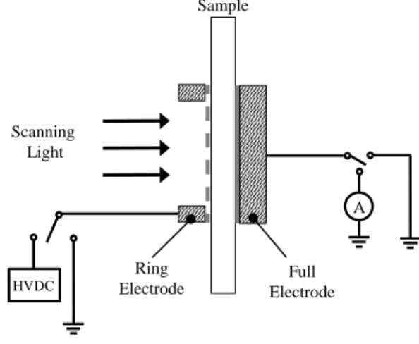
Fig. 1. PSD Circuit diagram Scanning Light A Ring Electrode Full Electrode HVDC Sample
Photo-stimulated Discharge Current Measurements
on Biaxially Oriented Polypropylene Thin Films
(BOPP)
L. Boudou
1, F. Zheng
2and G. Teyssedre
11
Laplace, CNRS and University of Toulouse, France
2Department of Electrical Engineering, Tongji University, Shanghai, China
Abstract- The photo-stimulated discharge method (PSD) is a very good tool to estimate charge trap energy levels in transparent or semi-transparent materials. Its advantage, when compared to thermally stimulated discharge (TSD), is to probe deeper charge traps without any thermal effect that can affect the material microstructure and the charge stability. In this work, PSD measurements were performed on biaxially oriented polypropylene films. The PSD spectrum shows two peaks located at 400nm and 240nm scanning light wavelength. The effect of the electrode structure (fingered vs. continuous electrodes) and the effect of applied field intensity are discussed.
I. INTRODUCTION
The interest of studying charge transport and trapping in dielectric materials has continuously increased over the past decades. Among the experimental methods that allow investigating charge trapping phenomena, those providing access to the distribution of trap levels are not numerous. The most used ones are probably the Thermally-stimulated discharge method (TSD) and the Photo-stimulated discharge method (PSD). TSD has the advantage to be a quick and useful method that allows to probe both dipolar processes and trapped charge release during a temperature ramp-up. Associated with space charge measurement techniques it can allow to dissociate charge detrapping processes from relaxation of orientation polarization [1]. However, the main problems of TSD concern the temperature effect on the microstructure of the material during measurement (annealing effect), the fact that charge release may correspond to charge dissipation due to destruction of the trap due to chain motion rather than release of the charge by thermal activation and that TSD is not appropriated to deep traps probing in polymer materials, because the temperature increase is limited by the melting of the tested material. In addition, the kinetic analysis of TSD glow curves is not straightforward, especially if overlapping distributed processes are at play. In the PSD method, introduced in the 1970s, the charge release is induced by irradiation of the sample with monochromatic light. This method is well adapted to estimate charge trap energy level in transparent or semi-transparent materials [2]. The progress in illuminating source development, especially in the deep-ultraviolet range (200-300 nm) allows probing deeper traps compared to PSD, without any detrimental effect on the sample microstructure. Nonetheless the interpretation of the
PSD data is sometimes difficult. Actually, the recorded PSD current can originate from space charge detrapping, but also from photoconduction effect, photoelectric effect or distorted by dipolar relaxations during measurement [3, 4].
The first part of this paper is dedicated to the description of the test bench including irradiation source characterization, electrode structure and experimental protocol description. In the second part the charge/discharge currents and the PSD spectra obtained on biaxially oriented polypropylene (BOPP) films for different applied voltage are presented and discussed.
II. METHODOLOGY A. PSD apparatus
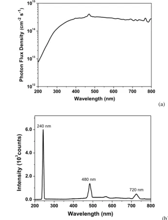
The circuit diagram for PSD measurement is shown in Fig 1. The monochromatic light is produced by a 150W Xenon arc lamp associated with a monochromator equipped with a 300nm-blaze grating (1200g/mm). The bandwidth of the monochromatic light can be controlled adjusting the input and output slits (2 mm for both in this study). All the experiments were performed in air atmosphere and at room temperature. The output power P(W) was measured as a function of the wavelength using a thermopile sensor (ref Newport 919P-003-10). Considering a monochromatic light and an irradiation spot of 3 cm in diameter at the sample surface, the photon flux density could be estimated, cf. Fig. 2(a). The flux is roughly constant in the 400 nm-800 nm range and decreases in the UV range when scanning down to 200 nm.
200 300 400 500 600 700 800 1012 1013 1014 1015 P h o to n F lu x D e n s it y ( cm -2 s -1) Wavelength (nm) (a) (b) Fig. 2. Photon flux density versus light wavelength (a) and 240 nm –
illuminating light characteristic
TABLE 1.
CHARACTERISTIC OF THE MONOCHROMATOR FOR A SELECTED WAVELENGTH OF 240 NM.
Fundamental Harmonic n=2 Harmonic n=3
Peak w.l. (nm) 240 480 720
Imax (counts) 6638 2001 1112
FWHM (nm)* 7 14 21
*Full width at half Maximum
200 300 400 500 600 700 800 0.0 2.0 4.0 6.0 In te n s it y ( 10 3 c o u n ts ) Wavelength (nm) 240 nm 480 nm 720 nm
In order to evaluate the wavelength bandwidth of light at the output of the monochromator, characterization at a 240 nm-fixed wavelength was performed using a spectrometer (model HR4000-UV-NIR from Horiba). The spectrum, shown in Fig. 2(b) –see also Table 1, reveals the fundamental peak located at 240 nm as well as the harmonic peaks, which are not filtered in our apparatus. The bandwidth obtained using an exit slit of 2 mm is 7 nm (it can be decreased by using a more narrow slit, but this is detrimental to the output power). The harmonics produced by the monochromator have non-negligible amplitude. However, as the scanning is achieved from large to small wavelength, their contribution has no real effect on the measured PSD spectra.
The samples are previously charged under DC voltage. During conditioning, the charge and discharge current are registered using a Keithley 617 electrometer connected to the back electrode. In this configuration the polarization currents are positive (for a positive DC voltage applied), and depolarization currents are negative. For clarity, the PSD
spectra are presented in positive values, taking the opposite sign of the PSD current recorded during the measurement.
B. Material
The material used in this study is a bi-oriented polypropylene (BOPP) film of 18 µm in thickness provided by Kopafilm, Germany. The films are provided with rough surfaces to promote impregnation of capacitors. Test samples were BOPP discs of 8 cm in diameter, with gold electrode sputtered on each face. For the electrode facing to the scanning light (termed as the front side), we used a fingered electrode having a diameter of 4 cm (Fig. 3) with a thickness of 50 nm. For the electrode connected to the ammeter (termed back electrode), we used a sputtered full gold electrode with a thickness of 50 nm from measurements on gold layers processed with the same sputtering equipment, the transmittance of a 50 nm-gold layer is estimated to less than 30% [5] in the UV wavelength range.
C. Measurement Protocol
The experimental protocol used is represented in Fig. 4. The samples were polarized at constant voltage (1 kV, 2 k V or 3 kV corresponding to electrical fields of 55 kV/mm, 110 kV/mm and 167 kV/mm respectively) during 30 min. After the polarization step the sample was short-circuited during 30 min. before the light irradiation starts and the discharge current was measured. The short circuit step is to complete fast relaxation processes in order for the PSD spectrum to be initiated with a negligible current. The PSD current is recorded during the light scanning from low energy (590 nm)
Fig. 3. Electrode structure. (a) Finger electrode (b) Full electrode
Fig. 4. Experimental protocol
Back Electrode Front Electrode BOPP Film (a) (b) 0 30 60 90 C u rr e n t W a v e le n g th V o lt a g e Time (min) 0 Vp 0 200 nm 590 nm
to high energy (200 nm) with a scanning rate of 24 nm/min. Scanning at longer wavelength did not produce significant current and could possibly heat the sample.
III. RESULTS AND DISCUSSION A. Polarization and depolarization current
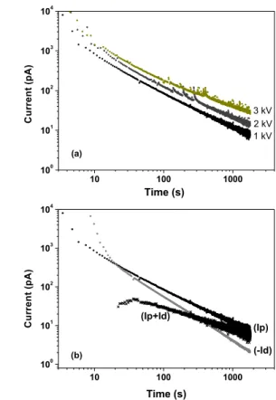
Fig. 5 (a) shows the transient current registered during the polarization step, for different applied voltages. It shows that the steady-state current is not reached after 30 minutes of polarization. It is then difficult to make use of the current versus voltage characteristic in order to identify the conduction mechanism at play in the field range explored.
The threshold field between ohmic and nonlinear behavior can be estimated at about 40 kV/mm from charging currents measured over 24 h [6]. With using shorter voltage steps of 5 min, a steeper increase of the current occurs beyond 100 kV/mm and weak electroluminescence was detected for fields beyond 200 kV/mm under DC stress [7], meaning that there is not a great amount of charge recombination events. This is consistent with the fact BOPP is known to be highly resistive. In the field range investigates herein, 50 to 150 kV/mm, charge injection from the electrodes and trapping within the polymer bulk are probably the main mechanisms at play. Furthermore, Fig. 5(b) shows that there is no superposition when polarization and depolarization current are compared, even at the lower applied field, meaning that the contribution from dipolar mechanisms to the registered current is negligible in the invstigated field range.
B. PSD spectra
The blank PSD spectrum, performed without any stress previously applied to the sample, is flat, cf. Fig .6. When using a full semi-transparent Au electrode with a thickness of 18 nm facing to the light beam, the PSD spectrum show two peaks (results not shown here) located at around 220 nm and 400 nm, but their amplitudes are small, even at high voltage. In order to improve the signal-to-noise ratio, the incident light intensity can be increased by increasing the width of input and output slits, with a loss of resolution in wavelength. Another way is to use a fingered electrode facing to the irradiation light. The current signal is higher because of higher light penetration within the material bulk. On the other hand, one of the indirect effects of using such fingered electrode is that electric field is enhanced locally due to edge effects, and as a consequence charge injection and trapping at these “hot points” can be substantially increased [8].
On the PSD spectra shown in Fig.6, two current peaks are observed, located at approximatively at 400 nm and 220 nm. The peaks are superimposed to a baseline current, voltage dependent, which is in the continuity of the transient current curves shown in Fig. 5a. Note here that the PSD spectra were not corrected for the output power of the monochromator. Considering Fig.2a, The amplitude of the 220 nm peak would be magnified by at least one decade in respect to the peak at 400 nm after such correction. The PSD intensity increases with the voltage applied during the polarization step increases, the intensity of the peak located at 220 nm being higher when compared to the peak located at 400 nm. One notices that the intensity is very weak for 1 kV polarization; it increases substantially for 2 and 3 kV, revealing that the threshold for massive charge injection has been reached. For both peaks, the wavelength position is not affected when the voltage is increased. Furthermore, the peak current Imax (taken between
the maximum and the baseline of the peak) does not increase linearly with the applied voltage (cf. insert of Fig. 6.). The shapes of the two recorded peaks are different. The 400 nm-peak is broad (spreading from 480 nm to 360 nm with a FWHM of 50 nm) and asymmetric. The 220 nm-peak is
Fig. 5 (a) Transient current recorded during polarization step for 1 kV, 2 kV and 3 kV applied voltage and (b) Polarization current (Ip) and
depolarization current (-Id) for 1 kV applied voltage.
10 100 1000 100 101 102 103 104 3 kV 2 kV C u rr e n t (p A ) Time (s) 1 kV (a) 10 100 1000 100 101 102 103 104 (Ip+Id) C u rr e n t (p A ) Time (s) (-Id) (Ip) (b)
Fig. 6. PSD spectra of 18 m-thick BOPP recorded after polarisation process under voltage of 1 kV, 2 kV and 3 kV, using fingered electrode as
front electrode. Inset: voltage dependence of PSD peaks.
600 500 400 300 200 0 20 40 60 80 0 1 2 3 4 0 40 80 0 kV 3 kV 2 kV P S D c u rr e n t (p A ) Wavelength (nm) 1 kV E (eV) 400nmImax) x10 220nm Imax) P S D C u rr e n t P e a k ( p A ) Voltage (kV) 2 3 4 5 6 7 8
narrower and asymmetric. The rate of the current increase with decreasing wavelength is also different when the two peaks are compared, and estimated at 2.74 pA/nm for the 220 nm-peak and 0.045 pA/nm for the 400 nm-peak for the PSD spectrum obtained after polarization under 3 kV. These differences are indications that the two peaks originate from different mechanisms.
The 220 nm-peak is located in a wavelength range wealthy in optical signature when considering the UV-absorption spectrum of BOPP measured at room temperature [9]. This spectrum shows an absorption maximum at 200 nm and a first shoulder at 230 nm, typical of π→π* transitions in C=C double bonds. A second shoulder at 280 nm is rather due to the n → π * transition in carbonyl compounds. These two regions (230 and 280 nm) are those providing maximum in photoluminescence of polyolefins [9]. The 400 nm-peak does not correspond to known absorption band in polyolefins in general, neither of the BOPP investigated herein. Either it corresponds to some additive that could efficiently trap charges, or possibly to localized states formed under the effect of space charge [10]. Another feature not to neglect is the possibility that electrons be generated from the illuminated electrode by photo-generation [8]. It is difficult at the present stage to identify the physical and/or chemical origin of the traps responsible of the PSD signature of BOPP film without any further investigations. A further point to address is the large difference in energies obtained by PSD (over 2 eV) compared to TSD (of the order of 1eV) or for charge detrapping in polyolefins [11].
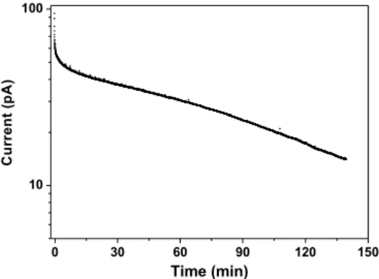
C. Photo-discharge transient current
Another way of analyzing the discharge consists in measuring the current decay as a function of time under fixed wavelength. Fig. 7 shows the result obtained with charging under 3kV with the same protocol as previously and following the decay. The current shows a fast drop in the first minutes followed by a much slower decay lasting for several hours after the irradiation light on. Charges released probably follow multiple trapping on their flow back to the electrodes (or same for photo-generated carriers to drift into the bulk). This means that during scanning procedure used in the classical PSD method, the detrapping of charges is not complete for a given
wavelength. This could bring some confusion when PSD spectra are analyzed.
IV. CONCLUSIONS
The use of fingered electrode as front electrode for PSD method allows to increase the current intensity without loss of wavelength resolution. Injection and trapping phenomena are enhanced due to edge effects but the local electric field value is difficult to control in this configuration. The PSD spectrum of 18 m thick BOPP film shows two peaks located at 400 nm and 240 nm scanning light wavelength. The blank PSD being flat, the PSD current recorded in short-circuit conditions is most probably linked to charge detrapping phenomena. However, the interpretation of the peak wavelength positions is not trivial and further work is needed to identify the physical and/or chemical origin of the traps responsible of the PSD signature of BOPP film.
ACKNOWLEDGEMENT
The research is supported by the program IDEX Actions
Thématiques Stratégiques ATS 2015 of the Université de
Toulouse under project SEPHIR (2016-066-CIF-D-DRVD). REFERENCES
[1] M. Q. Hoang, L. Boudou, S. Le Roy and G. Teyssedre, "Dissociating space charge processes from orientation polarization in Poly(ethylene naphthalate) films", J. Phys. D: Appl. Phys., Vol. 47, p. 455306, 2014. [2] A. Mellinger, F. C. Gonzalez and R. Gerhard-Multhaupt,
"Photostimulated discharge in electret polymers: an alternative approach for investigating deep traps", IEEE Trans. Dielectr. Electr. Insul., vol. 11, p. 218, 2004.
[3] F. Zheng, W. Li, M. Gu, Z. An and Y. Zhang, "Photo-stimulated discharge current in polyimide films", IEEE Trans. Dielectr. Electr. Insul., vol. 24, p. 1802, 2017.
[4] L.J. He, X. Yang, H.Q. Niu, Z.H. Yuan, D.W. Li and C.T. Chen, "Influence of photoconductivity on the study of trap levels in polyimide films by photo-stimulated discharge", Modern Phys. Lett. B, vol. 30, p 1650410, 2016.
[5] B. Qiao,"Electrical ageing of insulating polymers: approach through electroluminescence and cathodoluminescence analyses, PhD Thesis, university of Toulouse, 2015.
[6] H. Li, Z. Li, F. Lin, D. Liu, B. Wang, Y. Chen, L. Dai and S. Fan, "Electrical conduction of metallized BOPP films based on revised Poole-Frenkel effect", J. Electrostatics, vol. 71, p.958, 2013.
[7] B. Qiao, C. Laurent and G. Teyssedre, "Evidence of exciton formation in thin polypropylene films under AC and DC fields and relationship to electrical degradation", IEEJ Trans. Fundam. Mater., vol. 136, p.74, 2016.
[8] P. Ma, Y. Zhang, S Holé, F. Zheng, M. Gua and Z. An, "Analysis and interpretation of photo-stimulated discharge spectrum for polypropylene films under different electric and geometrical conditions", J. Electrostatics, vol. 84, p.128, 2016.
[9] B. Qiao, G. Teyssedre and C. Laurent, "Field- and electron beam-induced luminescence phenomena in polypropylene thin films", Proc. Int. Conf. Properties and Applications of Dielectric Materials (ICPADM), Sydney, Australia, p. 196, 2015.
[10] C. B. Duke, "Optical absorption due to space-charge-induced localized states", Phys. Rev., vol. 159, p.632, 1967.
[11] Y. Suzuoki, T. Mizutani, Y. Takai and M.Ieda, "Investigation of Carrier Traps in Polyethylene by PSDC and TSC", Jpn. J. Appl. Phys., vol. 16, p. 1929, 1977.
Fig. 7. Transient photodischarge current under continuous illumination at 220nm. Sample previously polarized under 3kV for 30min.
0 30 60 90 120 150 10 100 C u rr e n t (p A ) Time (min)