HAL Id: hal-01430587
https://hal.archives-ouvertes.fr/hal-01430587
Submitted on 7 Mar 2018HAL is a multi-disciplinary open access
archive for the deposit and dissemination of sci-entific research documents, whether they are pub-lished or not. The documents may come from teaching and research institutions in France or abroad, or from public or private research centers.
L’archive ouverte pluridisciplinaire HAL, est destinée au dépôt et à la diffusion de documents scientifiques de niveau recherche, publiés ou non, émanant des établissements d’enseignement et de recherche français ou étrangers, des laboratoires publics ou privés.
Three Dimensional Visualization of Electromagnetic
Fields from One Dimensional Nanostructures
Charudatta Phatak, Aurélien Masseboeuf, Ludvig de Knoop, Christophe
Gatel, Martin Hÿtch
To cite this version:
Charudatta Phatak, Aurélien Masseboeuf, Ludvig de Knoop, Christophe Gatel, Martin Hÿtch. Three Dimensional Visualization of Electromagnetic Fields from One Dimensional Nanostructures. Microscopy and Microanalysis, Cambridge University Press (CUP), 2015, 21 (S3), pp.1977–1978. �10.1017/S1431927615010661�. �hal-01430587�
Three Dimensional Visualization of Electromagnetic Fields from
One Dimensional Nanostructures
Charudatta Phatak1, Aur´elien Masseboeuf2, Ludvig de Knoop2, Christophe Gatel2,3, Martin J. H¨ytch2 1Materials Science Division, Argonne National Laboratory, Lemont, IL 60439, USA
2CEMES-CNRS, 29, rue Jeanne Marvig, FR - 31055 Toulouse, France 3Universit´e Paul Sabatier, F-31000 Toulouse, France.
One-dimensional (1D) nanostructures have been regarded as the most promising building blocks for nanoelectronics and nanocomposite material systems as well as for alternative energy applications [1]. Magnetic nanowires with circular cross-section, are of utmost importance from theoretical and tech-nological aspects [2]. 1D carbon-based nanostructures such as carbon nanotubes are amongst the best candidates for field emission displays and new high-brightness electron sources [3]. The confinement effects in 1D nanostructures can alter their properties and subsequently their behavior significantly. Hence it is necessary to understand the strong effect of their size on their three-dimensional (3D) prop-erties such as the magnetic and electric fields associated with nanowires and nanotubes completely before they can be used in applications. There are currently very few methods, which have the capa-bility to visualize the complete 3D fields associated with nanowires. In this work, we show that using a combination of symmetry arguments and electron-optical phase shift data obtained using TEM, it is possible to recover the entire 3D magnetic or electric field in and around nanowires and nanotubes from a single image.
The phase change ϕe+ϕmof an electron wave traveling through a thin foil can be expressed in terms of tomographic quantities [4]. The phase shift can be recovered experimentally using various techniques such as transport-of-intensity based methods or off-axis electron holography. Nominally, determining the 3D magnetic field or 3D elestrostatic potential requires recording a series of phase shift images as the sample is tilted about its axis. However, in a 1D nanostructure such as a nanocylinder that is uni-formly magnetized along its long axis, the magnetic field possesses cylindrical symmetry with respect to the long axis. Similarly, carbon nanotubes under applied bias exhibit a cylindrically symmetric potential and electric field. Exploiting these conditions of cylindrical symmetry, we can reconstruct the full 3D magnetic or electric field associated with a nanowire from a single phase image using the inverse Abel transform. Simulations were performed for a uniformly magnetized sphere, which also possesses cylindrical symmetry to analyze the fidelty of the reconstruction algorithm. Fig. 1(a) shows the magnetic phase shift of such a uniformly magnetized sphere, (b) shows the derivative with respec-tive to the horizontal axis (∂ϕm/∂x) showing the cylindrical symmetry, and (c) the 3D reconstructed magnetic induction using the single image method developed in this work.
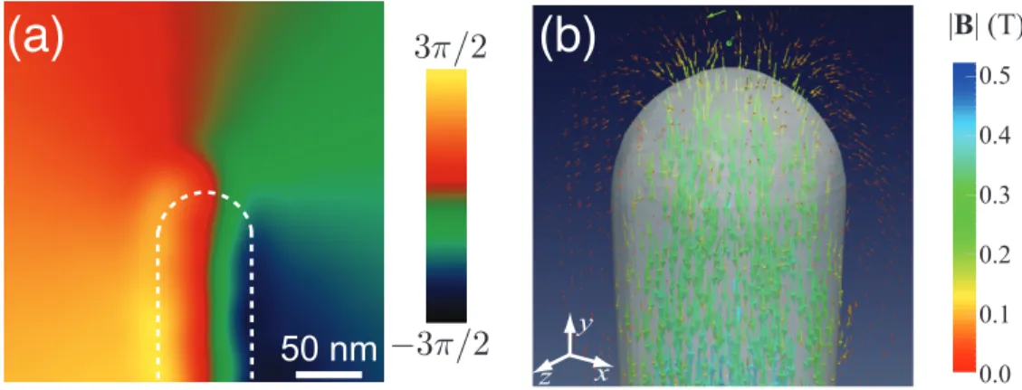
Experiments were performed on nickel nanowires that were uniformly magnetized to reconstruct the 3D magnetic induction. Similarly the 3D electric field was reconstructed from in-situ biased carbon cone nanotips under varying applied bias. The phase shift was recovered using off-axis electron holog-raphy in a FEI Tecnai F20 TEM operating at 200 kV using the first transfer lens of the Cs-corrector as a Lorentz lens. The magnetic phase shift was obtained from the Ni nanowire by recording the phase shift images with the sample as-is and rotating it by 180◦ about its axis and then subtracting the two
phase shifts. Fig. 2 (a) shows the magnetic phase shift of the Ni nanowire and (b) shows the recon-structed 3D magnetic induction. We will further discuss the details of the application and limitation of this method to reconstruct the 3D electromagnetic fields.
References
[1] C. M. Lieber, Solid State Communications, 107, 607 (1998).
[2] C. Chappert, A. Fert, F. N. Van Dau, Nature Materials, 6, 813 (2007).
[3] N. de Jonge, Y. Lamy, K. Schoots, T. H. Oosterkamp, Nature, 420, 393 (2002). [4] C. Phatak, M. Beleggia, and M. De Graef, Ultramicroscopy, 108, 503 (2008).
[5] This work was support by U.S. Department of Energy (DOE), Office of Science, Materials Sci-ences and Engineering Division.
By 0.8 0.2 0.0 -0.2 0.4 0.6 (a) (b) (c) y x z
Figure 1: (a) shows the magnetic phase shift image of a uniformly magnetized spherical nanoparticle, indicated by the dashed line, and magnetization vector is indicated by the blue arrow, (b) the derivative of the magnetic phase shift with respect to x showing the symmetry about the vertical axis of the image, and (c) the 3D reconstructed magnetic induction.
(a)
|B| (T)50 nm
x y z 0.0 0.5 0.2 0.3 0.4 0.1(b)
Figure 2: (a) shows the experimentally recovered magnetic phase shift from a Ni nanowire. The dotted lines indicate the border of the nanowire. (b) the 3D reconstructed magnetic induction from the nanowire.