HAL Id: hal-01489400
https://hal.archives-ouvertes.fr/hal-01489400
Submitted on 1 Mar 2018
HAL is a multi-disciplinary open access
archive for the deposit and dissemination of
sci-entific research documents, whether they are
pub-lished or not. The documents may come from
teaching and research institutions in France or
abroad, or from public or private research centers.
L’archive ouverte pluridisciplinaire HAL, est
destinée au dépôt et à la diffusion de documents
scientifiques de niveau recherche, publiés ou non,
émanant des établissements d’enseignement et de
recherche français ou étrangers, des laboratoires
publics ou privés.
A review of molecular beam epitaxy of ferroelectric
BaTiO3 films on Si, Ge and GaAs substrates and their
applications
Lucie Mazet, Sang Mo Yang, Sergei Kalinin, Sylvie Schamm-Chardon,
Catherine Dubourdieu
To cite this version:
Lucie Mazet, Sang Mo Yang, Sergei Kalinin, Sylvie Schamm-Chardon, Catherine Dubourdieu. A
review of molecular beam epitaxy of ferroelectric BaTiO3 films on Si, Ge and GaAs substrates and
their applications. Science and Technology of Advanced Materials, National Institute for Materials
Science, 2015, 16 (3), pp.036005. �10.1088/1468-6996/16/3/036005�. �hal-01489400�
Science and Technology of
Advanced Materials
FOCUS ISSUE REVIEW • OPEN ACCESS
A review of molecular beam epitaxy of ferroelectric
BaTiO
3
films on Si, Ge and GaAs substrates and
their applications
To cite this article: Lucie Mazet et al 2015 Sci. Technol. Adv. Mater. 16 036005
View the article online for updates and enhancements.
Related content
The 2016 oxide electronic materials and oxide interfaces roadmap
M Lorenz, M S Ramachandra Rao, T Venkatesan et al.
-New modalities of strain-control of ferroelectric thin films
Anoop R Damodaran, Joshua C Agar, Shishir Pandya et al.
-Emerging ferroelectric transistors with nanoscale channel materials: the possibilities, the limitations
Xia Hong
-Recent citations
Electrically tuned transmission and dielectric properties of illuminated and non-illuminated barium titanate thin film in terahertz regime
Jie Ji et al
-A review on all-perovskite multiferroic tunnel junctions
Yuewei Yin and Qi Li
-Controlled orientation of molecular-beam-epitaxial BaTiO3 on Si(001) using thickness engineering of BaTiO3 and SrTiO3 buffer layers
Min-Hsiang Mark Hsu et al
-Focus Issue Review
A review of molecular beam epitaxy of
ferroelectric BaTiO
3
films on Si, Ge and
GaAs substrates and their applications
Lucie Mazet
1, Sang Mo Yang
2,4, Sergei V Kalinin
2,
Sylvie Schamm-Chardon
3and Catherine Dubourdieu
1 1Institut des Nanotechnologies de Lyon, CNRS, Ecole Centrale de Lyon, Université de Lyon, 69134 Ecully, France
2
Center for Nanophase Materials Sciences, Oak Ridge National Laboratory, Oak Ridge, TN 37831, USA
3CEMES-CNRS, Université de Toulouse, 29 rue Jeanne Marvig, F-31055 Toulouse, France
E-mail:catherine.dubourdieu@ec-lyon.fr
Received 6 January 2015, revised 14 May 2015 Accepted for publication 14 May 2015 Published 30 June 2015
Abstract
SrTiO3epitaxial growth by molecular beam epitaxy (MBE) on silicon has opened up the route to
the monolithic integration of various complex oxides on the complementary metal-oxide– semiconductor silicon platform. Among functional oxides, ferroelectric perovskite oxides offer promising perspectives to improve or add functionalities on-chip. We review the growth by MBE of the ferroelectric compound BaTiO3on silicon (Si), germanium (Ge) and gallium
arsenide (GaAs) and we discuss thefilm properties in terms of crystalline structure, microstructure and ferroelectricity. Finally, we review the last developments in two areas of interest for the applications of BaTiO3films on silicon, namely integrated photonics, which
benefits from the large Pockels effect of BaTiO3, and low power logic devices, which may
benefit from the negative capacitance of the ferroelectric. Keywords: molecular beam epitaxy, ferroelectric, semiconductor
1. Introduction
Complex oxides exhibit a wide range of electrical, magnetic, optical and mechanical properties, which may even be cou-pled. This extraordinary wealth of physical properties offers a huge potential for developing new functionalities in devices that can address societal needs related to health, energy
efficiency or information and communication technologies. Ferroelectrics are particularly attractive for their applications in nanoelectronics, communication devices, electro –mechan-ical systems or sensors. However, in order to exploit their properties, complex oxide integration should be performed in a seamless manner on a semiconductor platform such as silicon or III/V substrates in order to be compatible with the mainstream nanoelectronic industry.
A great variety of complex oxides crystallize in a per-ovskite-type structure [1]. Tremendous progress has been achieved in the growth of oxides on oxide substrates (such as SrTiO3, LaAlO3, scandates, Al2O3, MgO…) in the past 15
years. Unit cell control (∼4 Å) of the growth can now be achieved. New phenomena arising from interfaces have emerged [2–5]. Progress in characterization techniques and modeling (density functional theory (DFT)) have allowed the |National Institute for Materials Science Science and Technology of Advanced Materials Sci. Technol. Adv. Mater. 16 (2015) 036005 (20pp) doi:10.1088/1468-6996/16/3/036005
4
Also with the Center for Correlated Electron Systems, Institute for Basic Science (IBS) and Department of Physics and Astronomy, Seoul National University, Seoul 151-742, South Korea.
Content from this work may be used under the terms of the
Creative Commons Attribution 3.0 licence. Any further distribution of this work must maintain attribution to the author(s) and the title of the work, journal citation and DOI.
study of physico-chemistry and mechanisms involved at the nanoscale and have resulted in a better understanding of the effect of size, strain and boundaries conditions on the prop-erties of complex oxides.
Integrating a perovskite oxide epitaxially on silicon is much more difficult and is still in its infancy, particularly regarding practical devices. One major difficulty for the epitaxy lies in the necessity to avoid the formation of an amorphous SiO2interfacial layer in thefirst stages of the growth. The first
direct epitaxy of a perovskite (SrTiO3) on silicon was realized
by molecular beam epitaxy (MBE) in 1998 [6]. MBE provides unique advantages to precisely construct, almost atom by atom, the oxide/semiconductor interface. Although this breakthrough achievement showed promise in integrating—in a monolithic way—oxides on a semiconductor platform, only a few suc-cesses have been reported in the past 15 years [7].
In this contribution to the focus issue on‘Properties and Applications of Perovskites’, we discuss the monolithic integration of complex oxides on semiconductors by MBE. We will illustrate the particular case of the ferroelectric BaTiO3compound. We review the work in the literature as
well as our own work. The crystalline structure and the fer-roelectric properties of BaTiO3heterostructures on Si, Ge and
GaAs are presented. Finally, an overview of perspectives and recent progress in ferroelectric oxide integration on semi-conductors for low power logic devices and integrated pho-tonics is provided.
2. MBE of complex oxides: a brief introduction to the technique
MBE was originally developed to epitaxially grow III–V compound semiconductors on a crystalline substrate [8,9]. It allows a control almost atom by atom of the growth in ultrahigh vacuum conditions. Progress in the MBE of oxides as well as in other deposition techniques took off in the late 1980s, after the discovery of the high-Tc superconductor
YBa2Cu3O7-δ. This implied the design of dedicated
metal-oxide growth MBE chambers. MBE of crystalline metal-oxides on silicon and on other semiconductor substrates has been developed in the late 1990s when thefirst epitaxy of SrTiO3
on Si was demonstrated [6]. This research benefited from the huge amount of efforts triggered by the microelectronic industry on the search for high-permittivity (highκ) oxides as a replacement to SiO2(or SiON) gate oxide in complementary
metal-oxide–semiconductor (CMOS) field-effect transistors. In the MBE of complex metal oxides, Knudsen effusion cells commonly used to evaporate the metals (Ba, Sr, Ti…) are focused onto a heated substrate under ultrahigh vacuum con-ditions (typically 10−10–10−9Torr). In the case of refractory elements, such as Ti, various means of evaporation have been reported: effusion cells, e-beam gun evaporation, Ti-Ball sub-limation source [10] and metal-organic vapor source [11,12]. Metal organic sources used in metalorganic chemical vapor deposition [13] such as titanium tetra isopropoxide Ti(OCH3H7)4 have been proposed in order to increase by
several orders of magnitude the vapor pressure of Ti as
compared to solid source and to have a beam flux that is relatively unaffected by the presence of oxygen in the chamber [12]. A wide window of growth parameters with self-regulating stoichiometry has been reported for SrTiO3films grown using
such a hybrid approach combining a conventional Sr effusion cell with a metalorganic precursor source for Ti [12].
For a given compound, deposition occurs by alternating the individualflux by means of shutters or by co-directing all fluxes simultaneously towards the substrate. Either molecular oxygen or atomic oxygen generated by a plasma source is typically used to provide the necessary oxygen to form the oxide. The oxygen pressure ranges typically from the 10−8to 10−5Torr. The background oxygen pressure plays a major role on the final stoichiometry, crystalline orientation and roughness of thefilms, as we will show later.
The reactivity of metal elements (in the chamber and in the sources) with the ambient oxygen (typically in the high 10−8–10−5Torr range) makes the control of the beam fluxes, and therefore composition, difficult. This is actually a major issue in the MBE of multicomponent oxides, which can usually accommodate a large range of non-stoichiometric composition. Indeed the physical properties of complex oxi-des are strongly dependent on the cationic and oxygen stoi-chiometry. Moreover, composition deviation may lead to the formation of spurious phases. A quartz crystal microbalance may be used to measure theflux of each atomic beam at the position of the substrate but it does not allow simultaneous monitoring of eachflux (it is not element specific) and cannot be employed for in situ control of the composition. In situ monitoring techniques have been proposed for composition control of multi-element oxides [14]. Among them, reflection high-energy electron diffraction (RHEED) is commonly used and has proven to be an effective in situ and real-time diag-nostic tool. A review article is proposed in [15] for the use of RHEED during complex oxide growth. It allows one to fol-low in real time the crystallinity of the depositedfilm and to adjust in real time the composition by tuning the impinging fluxes when additional spots originating from spurious phases are observed on the RHEED pattern.
Haeni et al [16] have proposed to use RHEED oscillations, both their shape and intensity, to control in real time the composition of multicomponent oxides such as SrTiO3. They
reported a control to within 1% of Sr:Ti ratio by monitoring the shuttered RHEED oscillations as the substrate surface is sequentially exposed to the Sr or Tifluxes. This precise control of monolayer (ML) doses of Sr and Ti has been used to suc-cessfully grow the first five members of the Srn+1TinO3n+1
Ruddlesden–Popper phases [17,18].
Various complex oxides have been grown by MBE. As mentioned, the development of oxide MBE started after the discovery of the high Tccuprate superconducting compounds
[19–28]. Since then, a variety of multiple-cation oxides have been epitaxially deposited by MBE on oxide substrates: SrTiO3, Ruddlesden–Popper phases, Bi4Ti3O12, Ba(Sr)TiO3,
SrVO3, GdTiO3, BiFeO3, LaAlO3, PbTiO3, LaCrO3, SrCrO3−δ,
La1−xSrxFeO3, LaTiO3.5, La2Zr2O7, LaNiO3, La2NiO4,
LaSrAlO4, and superlattices e.g. BaTiO3/SrTiO3 or PbTiO3/
On Si substrates, epitaxial SrTiO3films are used as templates
to grow a variety of complex oxides. BaTiO3has been the most
studied one by MBE. Apart from this compound, relatively few complex oxides (perovskite, spinel, pyrochlore phases…) have been grown by MBE on Si [55–62]. In many cases, the epi-taxial growth on the template layers is completed using other deposition techniques such as pulsed laser deposition, sput-tering, chemical vapor deposition or atomic layer deposition, as reported in [64–69] for BaTiO3.
A review of crystalline oxides on silicon is provided in [7]. The paper by Baek and Eom [63] gives a recent review of the epitaxial integration on silicon using SrTiO3templates of
the multiferroic BiFeO3, of the relaxor Pb(Mg1/3Nb2/3)O3–
PbTiO3 (PMN-PT) and of LaAlO3/SrTiO3 heterostructures
for 2D electron gas creation at their interface.
In the following, we focus on the MBE of the ferro-electric compound BaTiO3 on silicon, germanium and
gal-lium arsenide and on the related crystalline and ferroelectric properties.
3. MBE of BaTiO3 on semiconductors: growth and
crystalline structure
BaTiO3is a prototypical ferroelectric perovskite oxide, with a
Curie temperature of 120 °C. The ferroelectric tetragonal structure has lattice parameters of a = 3.994 Å and c = 4.0335 Å with space group P4mm (ICDD #83–1880) and the cubic paraelectric one has a lattice parameter of 4.006 Å with space group Pm-3m (ICDD #79–2263). The polarization is aligned along the c-axis of the tetragonal lattice. The tet-ragonality ratio c/a is 1.01, which is smaller than in Pb-based ferroelectrics such as PbTiO3 (c/a = 1.04). BaTiO3 is an
attractive ferroelectric for nanoelectronic, energy harvesting and photonic applications as will be discussed later in this article. It is a lead-free compound, which is an advantage regarding European regulation and industrial clean room compatibility.
While most MBE depositions of BaTiO3 on a
semi-conductor have been carried out on silicon, there is a growing interest in Ge and GaAs.
Silicon is the major semiconductor industry substrate. Current CMOS technologies are based on silicon wafers with size up to 300 mm and technologies on 450 mm wafer size are under development. Germanium (also a group IV semi-conductor) is of high interest forfield-effect transistors with p-type channel (p-FETs) due to the higher mobility of holes as compared to Si. Biaxially strained SiGe channels on Si have also recently attracted much attention for p-FETs. Both Si and Ge have a diamond structure with lattice parameter of 5.431 Å and 5.658 Å respectively. They form a solid solution Si1−xGexin the entire composition range (0⩽ x ⩽ 1).
The III–V gallium arsenide semiconductor has higher electron mobility than Si, which makes it attractive for n-FETs. It is today extensively studied as a channel for advanced CMOS technologies. GaAs has also a wider band gap than Si making it highly resistive if undoped. It is also more resistive to heat and radiation damage. It is suited for
many applications such as high frequency devices in com-munications or such as microwave and millimeter wave integrated circuits. Another advantage of GaAs is its direct band gap, which is of interest for optical applications. GaAs has a zinc blende structure with a lattice parameter of 5.653 Å.
BaTiO3deposition is mostly performed using an oxide
template since the direct epitaxy on semiconductors would result in a high defect density or in a non-appropriate film orientation. We thus describe the direct growth of SrTiO3
epitaxialfilms on semiconductors when relevant and their use for the epitaxial growth of BaTiO3.
In the following, BaTiO3 crystalline domains with
respectively the c-axis or the a-axis of the tetragonal cell being out-of-plane relatively to the substrate (001) plane are denoted respectively c-domains and a-domains.
3.1. MBE of BaTiO3on silicon
The lattice mismatch (aSi–aBTO)/aBTO, between BaTiO3and
Si(001) is about 4%, which is quite large and tends to favor a-axis growth when BaTiO3 is directly grown on Si [70].
Moreover, the large mismatch of the thermal expansion coefficients between Si (α = 2.6 × 10⁻⁶K−1) and BaTiO3
(α = 9 × 10⁻⁶K−1) leads to an in-plane biaxial tensile strain exerted on BaTiO3upon cooling, which favors a-axis growth.
In order to obtain c-axis oriented BaTiO3films on silicon, a
buffer layer that exerts a biaxial compressive in-plane strain should be used to overcome the biaxial tensile in-plane strain during cooling to room temperature [71]. SrTiO3 has been
widely used for such a purpose.
3.1.1. SrTiO3epitaxial templates on Si. The pioneering work of McKee and co-workers [6] opened up the route to the epitaxial growth of perovskite-type compounds on silicon and more generally to any oxide that could be epitaxially grown on bulk SrTiO3substrates.
SrTiO3is probably the most investigated epitaxial oxide
on silicon [7, 72–100]. Many studies have been directed towards understanding the crystalline and electronic structure of the film and of its interface with Si (or SiO2).
The epitaxial growth is realized by passivating the clean Si(001) 2 × 1 reconstructed surface by ½ of a ML of Sr. The Sr atoms are positioned between the Si dimers and prevent the surface from oxidizing. The native SiO2 can be in situ
thermally removed at high temperature; the clean Si (001) surface is then passivated by dosing the Sr metal to ½ ML. SiO2 can also be removed using a strontium-assisted
deoxidation process in which Sr acts as a catalyst to desorb the native oxide [74]; in this case, once SiO2 is fully
desorbed, more Sr is deposited until a 2 × 1 reconstructed surface appears on the RHEED, indicating the passivation of the Si(001) surface with ½ ML Sr coverage. The subsequent growth of SrTiO3 can be performed in different ways. The
first few MLs have to be grown at low temperature in order to avoid the oxidation of the interface.
Commensurate SrTiO3 thin films may be grown on Si
sequential deposition process’ [75,82]. The growth proceeds by alternating a low temperature deposition (∼200–300 °C) of 1–3 ML of a mainly amorphous Sr–Ti–O compound under an oxygen pressure of typically 10−8–1.5 × 10⁻⁷Torr, followed by an annealing step at higher temperature (580–700 °C) in ultrahigh vacuum conditions (<5 × 10⁻⁹Torr) to crystallize the SrTiO3phase. When grown in such conditions, there is no
interfacial SiO2oxide formed and SrTiO3films have in plane
lattice parameter commensurate to the Si 1 × 1 lattice. Relaxation occurs for ∼5 ML. Ferroelectricity in such ultrathin compressively strainedfilms has been reported [89]. The SrTiO3 deposition may also be performed by
growing at a higher temperature after the first few MLs of SrTiO3have been grown, with a low temperature growth/high
temperature post-anneal. In this case, the higher growth temperature (>450 °C) under oxygen results in an amorphous SiO2interfacial layer due to oxygen diffusion through thefilm
down to the interface with silicon. Since this amorphous layer occurs after the direct epitaxy of SrTiO3 on Si, it does not
disrupt the epitaxy of the SrTiO3film and subsequent oxide
growth. The epitaxial relationship between SrTiO3 and Si,
due to the lattice mismatch, is: [100]SrTiO3//[110]Si and
(001)SrTiO3//(001)Si.
In figure 1, we show a high resolution transmission electron microscopy (TEM) image of a SrTiO3film deposited
on Si substrate at a temperature of 400 °C under an oxygen partial pressure of P(O2) = 5 × 10⁻⁸Torr followed by a
crystallization step at 460 °C for 20 min under ultrahigh vacuum. We used a rapid cooling down procedure followed by a plasma anneal at 200 °C for 40 min in order to minimize the SiO2 regrowth while providing oxygen to the SrTiO3
lattice.
Choi et al showed that the SiO2interfacial layer thickness
increased during post-deposition annealing as P(O2) and/or
annealing time were increased (annealing at 650 °C under P(O2) from 2 × 10⁻⁷to 1 × 10⁻⁵Torr) [96] and that it can be
used to tune the strain relaxation of the SrTiO3layer. Before
annealing, the SrTiO3layers are expanded in-plane due to the
bi-axial tensile strain exerted by Si during cooling down. As
the oxygen partial pressure is increased during the post-deposition anneal, the SrTiO3 lattice parameters evolve
towards those of a cubic structure, which is concurrent to the SiO2interlayer thickness increase (figure2). Strain can be
tuned in the SrTiO3films within half a per cent, which can be
useful to adapt the lattice constants to the oxide to be grown on top [96].
Thick SrTiO3 films (100 nm) grown by MBE and
annealed at high temperature (900 °C) exhibit a full width at half maximum (FWHM) of the 002 rocking curve much narrower than the one of a bulk single crystalline substrate (the quality of which may, however, vary considerably depending on the quality of the original crystal) [90]. A TiO2
-terminated surface similar to the one typically prepared on bulk single crystalline SrTiO3substrates could be obtained by
buffered HF etching of the annealed films [90]. This procedure requires, however, thick films since interfacial reactions occur at high temperatures. On thinner 1–4 nm SrTiO3templates on Si, such a post-deposition annealing at
900 °C is not feasible. The surface may be TiO2terminated by
switching off the Sr beam and properly dosing the Tiflux.
3.1.2. MBE of BaTiO3 on SrTiO3-buffered Si. In their pioneering work [71], the group of Schlom used the solid solution Ba1−xSrxTiO3 as a buffer and could obtain fully
c-axis oriented BaTiO3films, while previous attempts to grow
BaTiO3 on silicon had lead to a-axis films. Both the
Ba0.7Sr0.3TiO3buffer and the BaTiO3 films were grown by
MBE. A thickness of about 10 nm was estimated for the buffer to be relaxed, which was the condition to obtain c-axis BaTiO3growth. In these conditions, a 10 nm BaTiO3film was
commensurate with the buffer (30 nm) and had an in-plane lattice parameter of 3.9996 ± 0.0005 Å, indicating that thefilm was predominantly c-axis oriented. This result was corroborated by optical second harmonic generation measurements. Shortly after, the group of Wessels [101] demonstrated the growth of c-axis BaTiO3 using a 5 ML
SrTiO3template (∼2 nm). By varying the film thickness, they
observed that the BaTiO3growth started as pseudomorphic
and that strain relaxation occurred at a critical value of 10 ML (∼4 nm). The out-of-plane lattice parameter was found to be fully relaxed at about 30–40 nm. They observe a mixed a- and c-oriented domain structure and the values extracted from aθ/ 2θ x-ray diffraction scan were a = 4.01 Å and c = 4.05 Å. Niu et al [102] reported the growth of a 40 nm BaTiO3fully c-axis
film on SrTiO3-buffered (5 nm thick) Si substrate, with lattice
parameters of a = 3.978 Å and c = 4.057 Å (c/a = 1.020). In [103], BaTiO3 films of thickness in the range
1.6–40 nm were studied with a 3.9–6.2 nm SrTiO3template.
X-ray diffraction and high-resolution TEM images indicated a pseudomorphic growth for the ultrathin 1.6 nmfilms. Films of thickness 8–10 nm were fully c-axis oriented with lattice parameters values close to the bulk ones (a = 3.993 Å and c = 4.038 Å with c/a = 1.011) while 16 and 40 nmfilms were composed of mixed c- and a-oriented domains. The local crystalline structure was determined by geometrical phase analysis (GPA) of high-resolution scanning transmission Figure 1.High-resolution TEM image of a SrTiO3thinfilm
electron microscopy (HR-STEM) images. Figure3shows the lattice parameter maps along the [100] and [001] as well as the lattice parameter profiles as a function of distance from the amorphous interfacial layer determined for a 16 nm BaTiO3
film deposited on a 3.9 nm SrTiO3buffer on Si. Infigure3(c),
the out-of-plane lattice parameter is larger than the in-plane one throughout the BaTiO3thickness, indicating fully c-axis
oriented domain. In other regions of the film (figure 3(d) orange profile), the film grows first c-axis and switches to a-axis after ∼4.0–4.5 nm. It is noticeable that the in-plane parameter increases continuously and therefore the switch from c- to a-domains is continuous. The tetragonality is maximum close to the interface with the SrTiO3 template
layer (e.g., a = 3.970 Å and c = 4.065 Å, c/a = 1.023) and decreases throughout thefilm thickness. Similar results were obtained on thicker films, in which the proportion of a-axis domains becomes predominant. Typical local lattice para-meters determined by GPA were a = 4.01 Å and c = 4.05 Å (c/ a = 1.010) for a 40 nm thickfilm. These values are similar to those reported in [101]. Edge dislocations were observed at the SrTiO3/BaTiO3 interface. The numerous profiles
per-formed on different areas of each sample suggested that the lateral scale of the c- and a-domains, when in coexistence, was similar or smaller than the 10–20 nm lateral distance between dislocations.
In the work by Abel et al [104], a MBE 8 nm BaTiO3
film grown on 4 nm SrTiO3 was found to be fully c-axis
oriented as well, with an out-of-plane lattice parameter close to the bulk c value. Similarly, in [105], we observed fully c-axis oriented films for 7 nm BaTiO3with lattice parameters
a = 3.996 Å and c = 4.027 Å. Droopad et al [106] reported c-axis orientation for a 8 nm film grown on a strained 2 ML (∼0.8 nm) SrTiO3 buffer, with an out-of-plane parameter
c = 4.032 Å. Lattice parameters reported by various groups in this thickness range (7–8 nm) are in good agreement [103–106].
Thicker films of 80–130 nm were studied for photonics applications as they are of potential interest for integrated electro–optic modulators and other photonic devices [107, 108]. A 130 nm thick BaTiO3 film was grown on
4 nm thick SrTiO3template and was fully a-axis relaxed with
lattice parameters a = 3.997 ± 0.005 Å and c = 4.032 ± 0.005 Å (c/a = 1.009) [107]. For 80 nm BaTiO3film on 8 nm SrTiO3
-buffered silicon-on-insulator (SOI) substrates, an out-of-plane lattice constant of 3.998 Å and an average in-plane lattice constant of 4.03 Å were reported, indicating relaxed a-axis film as well [108]. Atomic force microscopy (AFM) showed a smooth surface with a root-mean square (rms) roughness as low as 0.4 nm (one unit cell) [108]. Such thickfilms are a-axis oriented due to the tensile in-plane biaxial strain applied by the substrate during cooling down.
The critical thickness at which the orientation switches from c- to a-axis is determined by the competing influence of compressive stress from epitaxy and tensile stress from thermal expansion. Among other crucial influence might be the SrTiO3 buffer thickness and surface quality and the
composition of the BaTiO3 film. Slight cationic
off-stoichiometry may result in oxygen vacancies and structural defects that impact the lattice parameters and strain state [32]. Deposition conditions such as oxygen background pressure or deposition temperature have a major influence on the film growth and may impact thefilm composition. We have shown [105] that oxygen partial pressure P(O2) has a strong effect on
the morphology and crystalline orientation of 16–18 nm films. Increasing P(O2) in the range 1 × 10⁻⁷–3 × 10⁻⁶Torr leads to
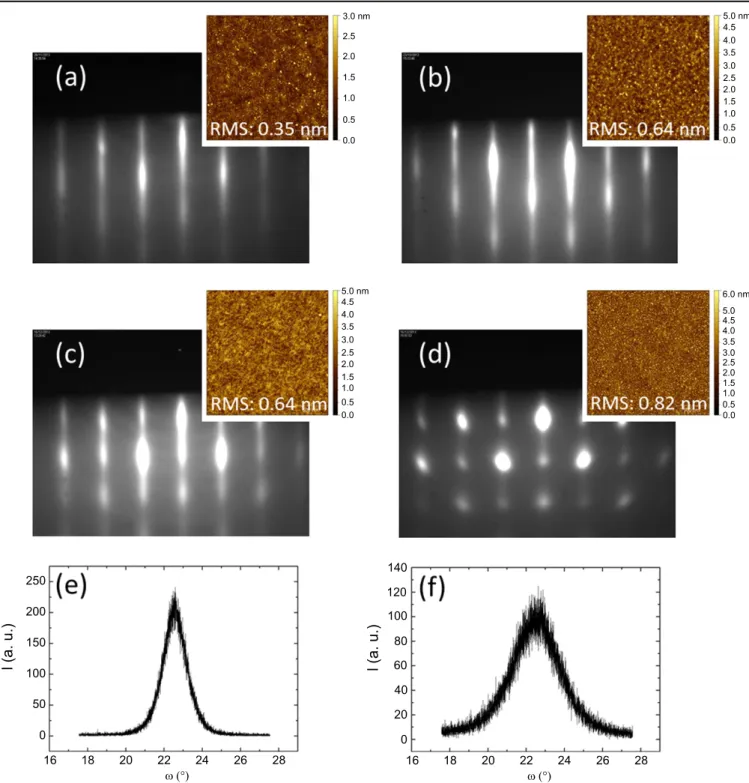
an increase of the surface roughness as shown infigures4(a)– (d) by the RHEED patterns and AFM images. The RHEED patterns for films grown at (1–5) × 10−7Torr exhibit well-contrasted streaky lines as expected for a 2D growth. Starting at 2 × 10⁻⁶Torr, partial or fully spotty patterns are recorded, which characterizes a rougher surface. From AFM, the rms increases from 0.35 nm (1 × 10⁻⁷Torr) to 0.82 nm Figure 2.(a) In-plane and out-of-plane lattice constants and (b) SiO2thickness as a function of oxygen partial pressure. Allfilms were
annealed at 650 °C for 30 min in different oxygen environments. Fromfigure 5 in [96]. Reprinted with permission from M Choi et al 2012 J. Appl. Phys.111 064112. Copyright 2012, AIP Publishing LLC.
(3 × 10⁻⁶Torr). X-ray diffraction indicated that increasing P(O2) promotes the growth of a-axis grains. Films grown at
1 × 10⁻⁷Torr were fully c-axis oriented. With increasing P(O2), the out-of-plane parameter was found to decrease
while the in-plane parameter increases. The FWHM of the rocking curves performed on the 002 peak (shown in figures 4(e)–(f)) is of 1.5° and 2.9° at 5 × 10⁻⁷ and 2 × 10⁻⁶Torr respectively (our lowest FWHM for a 002 rocking curve measured for ∼16 nm films is of the order of 0.7°). The ratio of the out-of-plane/in-plane parameters is lower than 1 for pressures equal or larger than 2 × 10⁻⁶Torr [105]. This trend was also reported for laser MBE-grown BaTiO3films on SrTiO3bulk substrates [109]. The effect of P
(O2) on the cationic Ba/Ti composition and on its impact on
the crystalline orientation should be further investigated. Oxygen stoichiometry is a major issue in MBE since oxidizing atmosphere and ultrahigh vacuum conditions are antagonistic. BaTiO3is grown either using molecular O2or
atomic oxygen often created by a radio-frequency plasma. A
post-deposition annealing might be performed in order to ensure sufficient oxidation of the films in order to reduce leakage currents and favor a stable ferroelectric polarization. Another issue related to the oxidation of thefilm is the SiO2
regrowth, which—depending on the application—might be detrimental for the properties. Thickness values of ∼3 nm [104] to ∼3.6 nm [103, 106] have been shown by TEM. Growth conditions and post-deposition annealing conditions have actually a strong impact on the interfacial SiO2
regrowth, as reported in [105] and illustrated in figure 5. We performed post-deposition annealing either in molecular O2 or in an oxygen plasma (typically 400 W). Figure 5(a)
shows an interfacial layer of∼2.5–3.0 nm for films grown at 450 °C under molecular O2 and slowly cooled
down (10 °C min−1) to room temperature under P(O2) = 1 × 10⁻⁵Torr. For the same growing temperature
and P(O2) conditions during the growth but a different post
annealing using a rapid cooling down under ultrahigh vacuum followed by a plasma anneal at 200 °C for 40 min, the SiO2
Figure 3.Strain analysis in a 16 nm BaTiO3/SrTiO3/amorphous interfacial layer (silicate and SiO2) stack. (a), (b) Maps of in-plane (a) and
out-of-plane (b) lattice parameters determined from GPA of HR-STEM images. (c)–(e) Lattice parameter profiles as a function of distance d from the interface between the amorphous interfacial layer and the crystalline SrTiO3layer, determined by averaging data from the black (c),
orange (d) and blue areas (e) in (a) and (b). Adapted fromfigure 2 in [103]. Reprinted by permission from Macmillan Publishers: C Dubourdieu et al 2013 Nat. Nanotechnol.8 748, copyright 2013.
layer is only ∼0.7–1.0 nm (figure 5(b)). In the same post-deposition annealing conditions but at a growing temperature of 525 °C, the SiO2is of∼1.7 nm as indicated in figure5(c).
The use of an atomic oxygen plasma at low temperature clearly minimizes the interfacial layer regrowth [105]. A detailed study of the defect structure in the SrTiO3buffer and
BaTiO3 film is underway to determine the impact of the
processing conditions.
Figure 6 is a STEM high-angle annular dark field (HAADF) image of the sample shown in figure 5(b),
illustrating the high crystalline quality of the perovskite stack and sharp BaTiO3/SrTiO3 and SiO2/SrTiO3 interfaces. The
BaTiO3film is coherently strained to the SrTiO3buffer layer
with no dislocations observed at the interface or in the film thickness.
In view of the literature data and various processing conditions used by the different groups, particularly regarding the oxidizing atmosphere (atomic or molecular oxygen and partial pressure), there is a need to better understand how to precisely control c- versus a-axis orientation in epitaxialfilms
3.0 nm 2.5 2.0 1.5 1.0 0.5 0.0 5.0 nm 4.0 4.5 3.0 3.5 2.5 2.0 1.5 1.0 0.5 0.0 5.0 nm 4.0 4.5 3.0 3.5 2.5 2.0 1.5 1.0 0.5 0.0 6.0 nm 4.5 5.0 3.5 4.0 3.0 2.5 2.0 1.0 1.5 0.5 0.0 250 200 150 100 50 0 120 140 100 80 40 60 20 0 16 18 20 22 24 26 28 ω (°) 16 18 20 22ω (°) 24 26 28 l (a. u.) l (a. u.)
Figure 4.(a)–(d) RHEED patterns recorded along the [100] azimuth during BaTiO3growth at 450 °C under an oxygen pressure of (a)
1 × 10⁻⁷Torr, (b) 5 × 10⁻⁷Torr, (c) 2 × 10⁻⁶Torr, (d) 3 × 10⁻⁶Torr and corresponding AFM images of thefilm surfaces. (e)–(f) Rocking curve measured on the 002 peak for thefilms grown at (e) 5 × 10⁻⁷(FWHM = 1.5°) and (f) 2 × 10⁻⁶Torr (FWHM = 2.9°).
on Si as well as the defect chemistry, which further determine the ferroelectric properties of thefilms.
3.2. MBE of BaTiO3on germanium
BaTiO3 exhibits a much lower mismatch with Ge (001) as
compared to Si (001) (∼1.8% at room temperature), which allows the direct growth of high crystalline quality BaTiO3
without using a buffer layer. Moreover, Ge (001) is less prompt to oxidize than Si(001). However, in contrast to Si, the lattice mismatch with Ge leads to an in-plane tensile strain, which is not in favor to c-axis growth. In addition, the thermal expansion mismatch between BaTiO3and Ge imparts
an in-plane tensile stress to thefilm upon cooling down (Ge: α = 5.9 × 10⁻⁶K−1).
McKee et al first demonstrated the epitaxial growth of BaTiO3directly on Ge with a perfect pseudomorphic
struc-ture [110]. However, suchfilms exhibited large leakage cur-rents (of the order of∼0.4 A cm−2at−1 V for a 25 nm thick film). The insertion of 6 MLs of BaO at the interface between Ge and BaTiO3led to a decrease of 6 orders of magnitude of
the leakage currents [110]. From photoelectron spectroscopy, a valence band offset of 2.8 eV for BaTiO3grown directly on
Ge was reported. About 10 years later, further experimental
works have been reported. The formation of alkaline-earth template layers on Ge(100) has been studied in detail in [111]. Both Ba and Sr have been used to promote the growth of BaTiO3 on Ge. Merckling et al grew BaTiO3 on Ge-on-Si
(001) substrate (1μm thick fully relaxed epitaxial Ge layer on Si) using ½ ML Ba as a passivation layer [112]. In a 12 nm BaTiO3film, they observed two different out-of-plane
para-meters of 4.072 and 4.060 Å and two in-plane parapara-meters of 4.05 and 4.01 Å. They attributed these parameters to the presence of a tetragonal phase (c-axis oriented) with para-meters close to the bulk one and to a cubic phase. Recently, Fredrickson et al [113] reported the growth of BaTiO3 on
bulk Ge (001) substrates using a careful Ge surface prepara-tion described in [114] and ½ ML Sr. The BaTiO3films were
deposited at 650 °C following three different stages (alter-nating the Ba and Ti fluxes) by progressively increasing the oxygen pressure from 1.5 × 10⁻⁷ to 5.10−6Torr [113]. The films grown in these conditions were a-axis oriented. An out-of-plane parameter of 3.995 Å and an in-plane parameter of 4.01 Å were measured for a 40 nm BaTiO3 film (averaging
the a and c values of the 90° in-plane domains) and the FWHM of the 200 rocking curve was ∼0.7°. From XPS measurements, the valence band offset between BaTiO3and
Ge was found to be 2.7 ± 0.1 eV, a value close to the one Figure 5.High resolution transmission electron microscopy images of BaTiO3/SrTiO3stacks grown under P(O2) = 1 × 10⁻⁷Torr for different
temperatures and post-deposition process. (a) 450 °C—slow cooling down procedure at P(O2) = 1 × 10⁻⁵Torr, (b) 440 °C—rapid cooling
down under ultrahigh vacuum (UHV) followed by annealing under an oxygen plasma (1 × 10⁻⁵Torr) for 40 min, (c) 525 °C—rapid cooling down under UHV followed by annealing under an oxygen plasma (1 × 10⁻⁵Torr) for 40 min. A SiO2interfacial layer between Si and SrTiO3
is formed upon SrTiO3annealing and BaTiO3growth and its thickness depends on the cooling down conditions. Horizontal dotted lines are
only to guide the eyes. Fromfigure 6 in [105]. Reprinted with permission from L Mazet et al 2014 J. Appl. Phys.116 214102. Copyright 2014, AIP Publishing LLC.
reported in [110]. Both in [110] and [113], high-resolution TEM images show an atomically sharp interface between Ge and BaTiO3.
In order to obtain BaTiO3 c-axis growth on Ge, it is
necessary to insert a buffer layer at the interface that can impart a compressive in-plane strain. Ngai et al [115] have grown a 20 nm tri-layer Ba1−xSrxTiO3stack—with decreasing
x values—as a buffer and have obtained c-axis oriented 40 nm thick BaTiO3films. The in-plane and out-of-plane parameters
were 3.987 Å and 4.040 Å respectively. Ponath et al [116] have grown c-axis BaTiO3films using a 2 nm SrTiO3buffer
on Ge (with ½ ML Sr prior to the SrTiO3buffer growth). The
lattice parameters were a = 3.96 Å and c = 4.06 Å for 16 nm thick BaTiO3. Both in [115] and [116], the comparison of the
x-ray diffractionθ/2θ scans clearly showed the impact of the buffer insertion on the BaTiO3crystalline orientation. In the
work of Ponath et al [116], STEM-HAADF images revealed that Ti atomic columns close to the top of the BaTiO3film are
shifted downward from the cell center, meaning a ‘down’ polarization, which is in good agreement with their DFT calculations. In contrast to this result and to the macroscopic mono-domain polarization of the as-depositedfilm, which is also shown to be oriented downward, the Ti atomic columns close to the SrTiO3film are found to be shifted upward. From
these images, it was also observed that no germanium oxide interfacial layer was formed at the interface between SrTiO3
and Ge [116]. The absence of low permittivity interfacial
layer makes this structure particularly suited for negative capacitance devices as those described later in section5.2.
As we have discussed the growth of BaTiO3on Si and
Ge, it is worth pointing out that SiGe alloy-based wafers should be of particular interest to engineer the strain and the interfacial layer in epitaxial BaTiO3.
3.3. MBE of BaTiO3on gallium arsenide
Although the lattice mismatch between GaAs and BaTiO3is
similar to the one between Ge and BaTiO3, we are not aware
of any report of direct epitaxial growth of BaTiO3on GaAs
by MBE. The epitaxial growth of BaTiO3on GaAs has been
performed via a buffer layer, in order to avoid interfacial reactions and to impart, like on Si and Ge, a compressive stress during cooling down in order to obtain c-axis oriented films (GaAs: α = 5.8 × 10⁻⁶K−1).
Various oxide buffers have been studied to grow crys-talline epitaxial oxides on GaAs (001). Laser MBE (base pressure 1 × 10⁻⁷Torr) [117, 118] or MBE [119,120] were used to grow MgO on GaAs for subsequent BaTiO3growth
by pulsed laser deposition. The following epitaxial relation-ship was obtained: MgO (001)//GaAs (001) and MgO [100]// GaAs [100]. MBE under molecular oxygen led to a reaction between Mg and GaAs and to a highly three-dimensional growth with a rough final surface morphology [119]. Fol-lowing the growth of SrTiO3on Si by MBE, routes have been
also developed to grow high quality SrTiO3films on GaAs.
3.3.1. SrTiO3epitaxial template on GaAs. SrTiO3has been
epitaxially grown by MBE on GaAs in the early 2000s using ½ ML Ti as a surface treatment (while ½ ML Sr is used on Si) [121, 122]. GaAs was first heated to about 600 °C in the presence of As4 flux to remove the native oxide layer. A
homoepitaxial GaAs layer (∼0.5 μm) was then grown. Prior to SrTiO3 deposition, ½ ML Ti was deposited at ∼300 °C.
Both As- and Ga-terminated GaAs (001) surfaces were used [121]. Sr and Ti were co-deposited on the Ti-passivated GaAs surface in conditions that could preserve the surface: similarly to the conditions used for SrTiO3 deposition on Si,
low-temperature (∼300 °C) and low 10−8Torr O2pressure. Both
temperature and oxygen pressure were slowly ramped up as the deposition proceeded. Similarly to SrTiO3deposition on
Si, SrTiO3was annealed after thefirst few MLs at ∼550 °C to
be fully crystallized. Once these first steps were completed, the growth of SrTiO3was then resumed at higher temperature.
SrTiO3grows on GaAs (001) with an in-plane 45° rotation of
the cell as well. From high resolution TEM, the interface was found to be abrupt, free of interfacial Ga-oxide [121, 123]. The electronic structure of the interface was investigated by x-ray and ultraviolet photoelectron spectroscopy [122,123]. The authors concluded that the Fermi level is pinned at the SrTiO3/GaAs interface when SrTiO3 is grown directly on
GaAs while it is unpinned if ½ ML Ti is used prior to SrTiO3
deposition. However, band bending in GaAs was found to be very sensitive to the annealing conditions making integration of such materials challenging since the integrity of the Figure 6.Scanning transmission electron microscopy high-angle
annular darkfield (HAADF) image of a BaTiO3/SrTiO3stack grown
on Si (001), indicating a sharp interface between SrTiO3and BaTiO3
interface could be strongly impacted by higher thermal budget steps required in device fabrication [122].
Other groups have reported the growth of SrTiO3 on
GaAs [124–127]. Wu et al performed the growth by laser MBE without Ti pre-deposition, by ablating a SrTiO3single
crystalline target [124]. Louahadj et al [125,126] performed the growth of SrTiO3 by MBE on c(4 × 4) As-terminated
GaAs (001) surface using ½ ML Ti prior to SrTiO3
deposition. Such layers were then used as a template for subsequent La0.7Sr0.3MnO3/PZT stack deposition by pulsed
laser deposition [126]. Contreras-Guerrero et al [127] studied the interface properties (Fermi level pinning) offilms grown in different oxygen conditions on c(4 × 4) As-stabilized GaAs (001) surface with ½ ML Ti pre-deposition: first, 2 nm of SrTiO3 was grown under molecular oxygen and then the
growth was continued either under molecular oxygen or under atomic oxygen. From room temperature photolumines-cence experiments, they reported that the density of interfacial defects increased when an oxygen plasma was used and that the Fermi level was pinned similarly to that of a GaAs layer with a native oxide. In situ photoemission experiments showed an increase in the Ga–O bonding at the interface when atomic oxygen was employed as well as As–As bonding (not present under molecular oxygen). This study showed the crucial role of oxygen species during growth in determining not only the stoichiometry of the oxide but also the interface structural and electrical quality.
3.3.2. MBE of BaTiO3on SrTiO3-buffered GaAs. BaTiO3has
been deposited on SrTiO3-buffered GaAs substrates by MBE
[106,128] or by laser MBE [129,130]. Huang et al reported the growth by laser MBE of c-axis orientedfilms [129]. They measured P–E loops using p-type GaAs as a bottom electrode and Pt as a top electrode. The loop exhibited a small concavity and was not saturated. The remanent polarization was 2.5μC cm−2 (with a maximum field of 600 kV applied during the measurement). Contreras-Guerrero et al reported the growth by MBE of BaTiO3on n + GaAs substrates with a
2 unit-cell (8 Å) SrTiO3buffer layer [128]. Ba and Ti were
co-deposited under molecular oxygen at 500 °C under P(O2)
of 1 × 10⁻⁷mbar (7.5 × 10⁻⁸Torr). Films of thickness 75 Å were c-axis oriented with an out-of-plane parameter of 4.032 Å.
Due to the interest in combining ferroelectrics with III–V compounds for optoelectronic applications, more work is to be expected in this area.
4. MBE of BaTiO3 on semiconductors:
ferroelectricity
In ferroelectric thinfilms, charges induced by the polarization at the top and bottom interfaces may not be compensated or only partially compensated, which gives rise to a depolar-izationfield. Boundary conditions are of utmost importance in determining the charge screening and depolarizationfield. It was shown [131] that the depolarization field arising in a
ferroelectric thin film sandwiched between semiconducting electrodes significantly modifies the transition temperature, the spontaneous polarization amplitude and the coercivefield. Under a critical film thickness, the switchable polar state becomes unstable [131].
While ferroelectricity of BaTiO3on oxide substrates has
been extensively studied, there are still few data for epitaxial films directly grown on semiconductors or on SrTiO3 (and
other dielectric) buffered-semiconductors.
For a metal-oxide-semiconductor capacitor, a hysteresis of the capacitance versus voltage (C–V) curve is expected if the oxide is ferroelectric, with a clockwise and anti-clockwise hysteresis on respectively p- and n-type silicon [132]. In [102] C–V measurements were performed on a 40 nm BaTiO3
c-axis oriented film deposited on SrTiO3-buffered Si with
100 × 100μm2 top electrode area (with a final ∼2 nm SiO2
interfacial layer regrowth). No ferroelectric hysteresis was observed, which was attributed to the limited oxygen pressure during the MBE growth [102]. However, such measurements are usually not appropriate to evidence ferroelectricity when an interfacial layer such as SiO2is formed. Indeed, the
vol-tage applied across the heterostructure is mainly dropped in this low-permittivity (low κ) interfacial SiO2 layer (κ = 3.9
compared to κ > 250 for BaTiO3 films). The silicon also
contributes to the total capacitance in depletion. Hence, it is not possible to reach an effective electrical field larger than the coercivefield to switch the thin ferroelectric layer.
Piezoresponse force microscopy (PFM) has emerged as a major technique for the study of ferroelectricity at the nanoscale [133–135]. The feasibility of domain writing/ reading, domain stability with time as well as the existence of piezoelectric hysteresis loop, checked by PFM, is an impor-tant necessary condition for ferroelectricity. However, it has been shown also that ionic and electrochemical phenomena may play a major role in scanning probe microscopy and can also lead to ferroelectric-like domain writing/reading and hysteresis loop [136,137]. For example, those features were observed in non-ferroelectric compounds such as crystalline LaAlO3/SrTiO3 heterostructures [138] or transition metal
oxides involved in memristive devices like TiO2 or SrTiO3
[139]. In case of conventional ferroelectrics such as BaTiO3
(well known in bulk), complementary structural information in thin films are useful. The dependence of the PFM signal with input voltage andfilm thickness should also be checked. Several groups have reported evidences by PFM con-sistent with ferroelectric switching for MBE-grown BaTiO3
on SrTiO3-buffered-Si [71,103–106], -Ge [116] and -GaAs
[106,128] substrates.
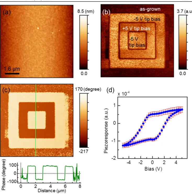
Figures 7(b)–(c) show typical PFM images (amplitude and phase respectively) for a 17 nm thick c-axis BaTiO3film
grown on SrTiO3(∼4 nm) on Si substrate, poled with −5 V,
+5 V, and −5 V over 6 μm, 4 μm, and 2 μm regions, respec-tively. Figure7(b) indicates similar amplitudes for +P and−P signals with a zero signal at the boundary between opposite poled regions and the graph offigure7(c) shows a clear phase difference of ∼180° between +P and −P regions. The as-deposited film (non-poled regions) does not appear mono-domain. A piezoresponse hysteresis loops consistent with
ferroelectricity is shown infigure7(d). The coercive voltages are of∼ −1.8 V and +2 V.
For BaTiO3grown directly on Ge substrates, no
ferroe-lectricity was reported from electrical or electromechanical measurements with an applied electricfield perpendicular to thefilm, which can be related to the fact that the growth is a-axis oriented [110,116]. In the work by Merckling et al [112] where a mixture of both c-axis tetragonal phase and cubic phase was reported, ferroelectricity was not studied. Ferroe-lectricity was reported for BaTiO3 c-axis oriented films on
(Ba,Sr)TiO3-buffered Ge [115,116]. Current versus voltage
curves were measured on capacitive structures with 40 nm BaTiO3deposited on a trilayer Ba1−xSrxTiO3buffer (20 nm)
stack and with top Pt electrodes, showing rectifying behavior [115]. A hysteresis consistent with ferroelectric switching was observed while no hysteresis was present for a heterojunction with a-axis 60 nm BaTiO3 directly on Ge [115]. In c-axis
16 nm BaTiO3film on 2 nm SrTiO3buffered-Ge [116], PFM
measurements indicated ferroelectricity with a coercive vol-tage of−4 V and +5 V. The non-poled regions (as-deposited Figure 7.(a) Atomic force microscopy topography and piezoresponse force microscopy (b) amplitude and (c) phase images for 17 nm thick BaTiO3/SrTiO3(∼4 nm) on Si substrate, poled with −5 V, +5 V, and −5 V over 6 μm, 4 μm, and 2 μm regions, respectively. The images were
collected over 8 × 8μm2areas. The bottom panel in (c) shows the line profile of phase signals, exhibiting clear phase difference of ∼180 degrees. (d) Piezoresponse hysteresis loop averaged over 10 × 10 points within 4 × 4μm2area. Error bars represent the dispersion of the signal measured at different locations on the sample surface.
film) were found to be mono-domain with the polarization oriented towards the STO/Ge substrate, which was in agree-ment with their theoretical calculations [116]. In addition to the ferroelectricity of BaTiO3, they also demonstrated the
ferroelectricfield-effect on the conductivity of the underlying Ge using microwave impedance microscopy [116].
Similarly, ferroelectricity in BaTiO3c-axisfilm (7.5 nm)
on 0.8 nm SrTiO3-GaAs substrate was inferred from PFM
measurements, with a repeatedly switchable polarization [128]. Patterns written and read were stable over ∼1 h. The coercive voltage was of the order of ±1–2 V. As-deposited films were poled with a polarization pointing towards the bottom interface [128].
Regarding the dependence of ferroelectricity on the thickness of ultrathinfilms, very limited work is reported. The thickness dependence in the range 1.6–40 nm of the PFM hysteresis loops was studied in [103] for BaTiO3on SrTiO3
-Si. Films of thickness 40 nm showed closed and saturated hysteresis loops. As the thickness was decreased down to 8 nm, the hysteresis loops were still well-defined with an elongated shape consistent with depolarization field effect [140]. An offset of the electromechanical signal was also observed as thickness decreased [103], which was attributed to imprint phenomenon originating from regions with non- or non-fully-switchable polarization. The coercive voltages for the 16 nmfilm were of the order of −10 V and +6 V [103], asymmetric and much larger than the ones obtained in the measurement shown in figure7 for a similar thickness (and for a same SrTiO3buffer layer thickness of 4 nm). This may
be due to the mixed c- and a-domain structure in the study reported in [103] while the film shown in figure7 is fully c-axis oriented. Fully c-c-axis oriented films of 8 nm (with a SrTiO3 buffer of 6.2 nm) had coercive voltages
of∼ ±4 V [103].
The ferroelectric polarization of thin and ultrathinfilms, the coercive field and the ferroelectric domain configuration are strongly dependent on thefilm thickness as well as on the boundary electrical conditions (nature of the electrodes) and polarization charge screening [141–146]. Garcia et al showed that an ultrathin 1 nm BaTiO3 film epitaxially grown on a
metallic manganite electrode is ferroelectric [145]. First-principle computations show that a net positive polarization exists in ultrathin SrTiO3, BaTiO3or PbTiO3epitaxialfilms
on silicon but that it cannot be switched as it is pinned by the interface [147]. We recently observed ferroelectricity in ultrathin BaTiO3 films down to 1.6 nm on SrTiO3-buffered
silicon [148] but with a strong imprint. For a same film thickness, the thickness of the SrTiO3 buffer layer and the
defect chemistry in such layer certainly play a major role in the polarization stability and amplitude in the BaTiO3 film,
which is currently under investigation.
Compared to the studies performed on BaTiO3 films
grown on oxide substrates (such as SrTiO3or NdGaO3bulk
crystals), a major difference on growing on semiconductors resides in the strong tensile strain imparted to thefilm during the cooling time, which may strongly affect the strain state, the defects, the crystalline phase(s) and the crystalline orientation(s) stabilized, which, in turn, impact the
ferroelectric properties. Ferroelectric domains in thin BaTiO3
films on silicon and other semiconductors need to be further explored in order to control their size and distribution.
5. Application of BaTiO3epitaxialfilms on
semiconductors
There are many applications for which ferroelectric epitaxial films on semiconductors can bring new functionalities. As a piezoelectric material, it can be integrated into microelec-tromechanical systems (MEMS) to design actuators, trans-ducers or sensors [149]. Non-volatile memories have been one of the major application areas of ferroelectrics [150]. Integration of a ferroelectric on silicon offers the ability to fabricate ferroelectric-FETs (FeFETs) as memory or logic devices. We will focus here on two recent areas that have generated several works on the monolithic integration of BaTiO3on semiconductors. One growingfield of interest is in
integrated photonics on silicon where building blocks such as electro–optic modulators could benefit from the high Pockels effect of BaTiO3. The other one is in the realization of low
power logic devices that has been suggested using the nega-tive capacitance of ferroelectrics.
5.1. Integrated photonics applications
Ferroelectrics are highly attractive for integrated optics to design waveguides with low losses and high bandwidth electro–optic modulators due to their large electro–optic coefficients, optical transparency and thermal stability [151]. In an electro–optic modulator, the phase of the light travelling through the crystal changes depending on the applied electric field. In bulk, lithium niobate LiNbO3is widely used as an
electro–optic medium. Waveguides are designed by modify-ing the composition of the substrate through diffusion or ion exchange [152] with resulting devices of millimeter or cen-timeter size. Integrating optical communication functionalities using thin films, especially on silicon platform, stimulates considerable research efforts. Indeed, integration of epitaxial films on silicon offers the ability to co-integrate optical functionalities with standard CMOS ones. Hybrid silicon/ lithium niobate optical microring resonators have been recently demonstrated [153–156]. However, the devices on silicon were fabricated from LiNbO3bonded to silicon using
complex techniques. Integrating epitaxial films in a mono-lithic route would offer much more flexibility. BaTiO3 is
particularly attractive for such purpose. It presents high refractive indices (no= 2.412 and ne= 2.36 at 633 nm) with
superior linear electro–optic properties compared to LiNbO3,
exhibiting one of the highest reported Pockels effect (r113= 14.5 pm V–1, r33= 103 pm V–1 and r42= 1700 pm V–1
at λ = 633 nm from [157]—similar values are also reported in [158]).
Several studies have been conducted on BaTiO3
epi-taxially grown on mainly MgO substrates (of lower optical index to allow optical confinement) to design waveguides and electro–optic modulators, either in ridge or strip-loaded
configurations and have shown the potential of this material [159,160]. Photonic crystal waveguide structures have been proposed to improve the performance of these devices [161– 163]. In a recent work, Li et al showed potential for achieving modulation at 65 GHz [164]. The epitaxial growth of BaTiO3
on SrTiO3 buffered-silicon offers a great potential for
per-forming integrated planar waveguides and electro–optic modulators as well as optical/ferroelectric combined func-tionalities. Abel et al reported recently for thefirst time the electro–optical properties of epitaxial BaTiO3 films on
SrTiO3/silicon [107]. They showed that BaTiO3 exhibit a
much higher effective Pockels coefficient of reff= 148 pm V–1
(λ = 1.55 μm), at least five times larger than the one of LiNbO3. Recently as well, the first monolithically integrated
BaTiO3 modulators on SOI substrates were reported
[108,165]. Since the silicon has a higher refractive index than BaTiO3, conventional ridge or strip waveguide configurations
are not suitable. The design is therefore that of a horizontal slot waveguide in which the a-axis oriented BaTiO3 layer
(80 nm) is comprised between the silicon substrate (110 nm Si from the SOI wafer) and an amorphous silicon layer (110 nm) [108]. The waveguide is patterned into the amorphous silicon layer and electrodes are patterned on each side of the wave-guide. Mach-Zehnder interferometers and microring resona-tors were demonstrated [108]. The authors reported an effective Pockels coefficient of reff= 213 ± 49 pm V–1. Similar
works pursuing the integration of BaTiO3 on silicon for
electro–optic modulators are ongoing [166].
5.2. Low power logic device applications
Power dissipation is one of the major issues that the CMOS nanoelectronic industry is currently facing. For decades, transistor dimensions have been scaled down at constant electric field following Dennard’s rules [167]. Such scaling implied that the supply voltage be reduced and as a con-sequence, that the threshold voltage Vthof the transistor be
reduced, leading after ∼2005 to unacceptable IOFF leakage
currents. In order to maintain a high enough ION/IOFF ratio
(while the subthreshold swing is thermodynamically limited to 60 mV/dec at room temperature), the scaling rules have therefore been changed to maintain a constant supply voltage. New materials (high-k oxides, III/V semiconductors) and architectures (fully-depleted SOI technology, multiple gate FETs…) have so far allowed us to keep miniaturization compatible with performance although clock frequency has to be limited. The impossibility to further reduce the operating voltage leads to a more general societal issue of energy consumption in a world where individual consumers now posses several electronic products. The percentage of energy consumption by individuals compared to industry keeps growing. There is an urgent need for low-power logic switches that could operate at∼0.2 V or below and several device concepts have been proposed [168].
In 2008, Salahuddin and Datta suggested that the nega-tive capacitance of a ferroelectric could be used to decrease the subthreshold swing below 60 mV/dec [169]. Although the state of negative capacitance of a ferroelectric is unstable, it
could be, however, possible to stabilize it by having in series a suitable positive capacitance. If the ferroelectric is inserted as a gate oxide in a FET and if its thickness is tuned to match the positive one of the silicon/dielectric (interfacial layer e.g.), the two contributions would cancel, leading to a very high effective capacitance. A small change in gate bias could therefore control a large change in the channel charge, meaning low voltage operation [169,170]. There have been many experimental and theoretical works since this initial proposal [171–183]. A sub-60 mV/dec subthreshold swing has been demonstrated in a FET using a ferroelectric polymer [171,177]. A thin AlSi metal was inserted between the fer-roelectric layer and the SiO2 interfacial layer, acting as an
internal electrode. Slopes ranging from 46 to 58 mV/dec were reported [171]. Several works have focused on combining ferroelectric and paraelectric epitaxial complex oxides in metal–insulator–metal (MIM)-type capacitive structures and demonstrated capacitance enhancement as compared to indi-vidual contributions, concluding to negative capacitance effect. Khan et al [174] reported an enhanced capacitance in a bilayer of Pb(Zr0.2Ti0.8)O3/SrTiO3 epitaxially grown on a
conducting SrRuO3 electrode at a temperature larger than
500 K. In 2014, two groups have reported room-temperature capacitance enhancement in BaTiO3-based epitaxial
hetero-structures on SrRuO3. Appleby et al [179] studied BaTiO3/
SrTiO3 bilayers and Gao et al [180] studied (LaAlO3/
Ba0.2Sr0.8TiO3) superlattices. Recently, Khan et al [181]
showed, for the first time, a direct proof for the negative capacitance in an epitaxial Pb(Zr0.2Ti0.8)O3film on a metallic
SrRuO3-buffered SrTiO3 substrate with a top Au electrode.
The capacitive structure was put in series with a large resis-tance in order to be able to measure the transient region when the ferroelectric passes through the unstable negative capa-citance state. As a voltage pulse was applied—while a regular capacitor would exhibit an increased voltage—the voltage across the capacitor was shown to decrease, thus indicating a negative capacitance transient [181].
These demonstrations of negative capacitance in MIM structures based on complex ferroelectric oxides give insight into the materials and show that the concept of negative capacitance may hold promise for FET devices. There is, however, no realization so far of a transistor fabricated with a ferroelectric epitaxial oxide on silicon. The reason is the major difficulty to integrate a complex oxide in a transistor following a conventional gatefirst route. One major issue is the integrity of the ferroelectric after the high-temperature anneal that is required to activate the source and drain regions (typically 1065 °C in the current technologies). A replacement gate route, which experiences a much lower thermal budget, should be followed to save the oxide properties. Another issue is the SiO2 interfacial layer that is formed during BaTiO3
growth on SrTiO3-Si substrates. When as little as few
Ang-ström of the low permittivity SiO2 dielectric is formed, it
requires the BaTiO3 layer thickness to be increased to few
hundreds or few thousands of Angström to reach the capa-citance balance. Finally, the concept of negative capacapa-citance FeFET (NC-FeFET) has limitations, which are discussed in details in [178]. One major issue is that the capacitance of the
silicon is strongly varying when going from depletion to inversion regimes while the capacitance of the ferroelectric is almost constant in the same voltage range, making the match impossible in the whole operating range. Another concern with using a ferroelectric complex oxide on silicon for NC purpose concerns the charge mismatch: when operating at low voltage, the charge change in Si between OFF and ON states is estimated to∼0.2 μC cm−2while the ferroelectric switches much more charges (typically 2–20 μC cm−2) as calculated in [178]. To address these issues, new devices concepts named ‘Quantum metal Fe-FET’ were proposed [178] and are shown in figure 8. A thin metal layer (called quantum metal) is inserted between the ferroelectric and the semiconductor and is intended to present a constant capacitance to the ferro-electric. It is designed such that its electron carrier density is low and can be modulated by the change in polarization of the ferroelectric layer. For a 2 nm metal layer, the carrier density should be of the order of 1021cm−3, which could be achieved using doped SrTiO3[45] or TaNxfilms [184]. Two different
devices were proposed [178]. In one case (device shown in figure8(a)), the currentflows in the semiconductor inversion layer like in a conventional FET, with the quantum metal’s modulated work function serving as the gate for the semi-conductor. In the case of the device infigure8(b), the current flows from the quantum metal into the silicon as in a Schottky barrier diode, with the barrier height being modulated by the FE gate electrode. A very steep slope in the channel charge versus gate voltage could be achieved, as shown infigure8(c) from the modeling of the device shown in figure 8(a). The charge changes by 11 orders of magnitude (700 mV change in surface potential) for a 20 mV change in the gate voltage, for
a slope of more than 500 decades V–1, or 2 mV/dec for the inverse slope. Hence, such devices are particularly attractive for future low power switches. However, technological challenges to fabricate such devices remain to be addressed.
6. Conclusions
We have reviewed studies on epitaxial BaTiO3 grown by
MBE on Si, Ge and GaAs semiconducting substrates. The SrTiO3 buffer layer epitaxially grown on these substrates
plays a key role to maintain a compressive strain to favor c-axis growth. High crystalline quality and ferroelectric prop-erties were demonstrated on the three substrates. Advancing ferroelectric applications requires better control and under-standing of the effect of oxygen and cationic composition on the ferroelectric properties. The domain pattern should be also further investigated in order to control their size and dis-tribution. Engineering of bottom and top interfaces with the ferroelectric layer could offer possible paths to such control. Relatively few works have been done in growing a top metallic electrode in situ in order to possibly control the domain structure. Wetting of Pt on BaTiO3(as a potential top
electrode) has been studied by DFT and experimentally [185]. DFT showed that despite a reasonable match of the lattice constant, the surface energy of both (100) and (110) Pt is too high to wet BaTiO3, which was confirmed by TEM
obser-vations, showing Volmer–Weber faceted islands, epitaxial with the underlying BaTiO3films [185]. Other metals such as
TiN or TaN widely used in nanoelectronics should be investigated.
Figure 8.Device structures for FeFET with quantum metal layer. The arrows indicate currentflow paths. (a) With and (b) without a thin insulator between the quantum metal and the semiconductor—(c) calculated Q–V curve for an FeFET as represented in (a)—DOS stands for ‘density of state’. Adapted from figures 4 and 6(a) in [178]. Reprinted with permission of IEEE (D Frank et al 2014 IEEE Trans. Electron Devices61 2145).
Regarding device fabrication, thick BaTiO3films show
promise in integrated photonics while thinfilms are of interest for low power logic devices. Heterostructures on Ge, in which no low-permittivity interfacial layer is formed, could be of particular interest to fabricate field-effect transistors with a steep subthreshold swing if the negative capacitance of the ferroelectric could be balanced with the one of the SrTiO3and
Ge contributions. Moreover, the ability to tune the SrTiO3
template to a conducting film using La3+ doping could be used for the design of the quantum metal field-effect transistor.
Progress in the epitaxial growth of perovskite compounds on semiconductors will also open up the route towards more complex heterostructures combining oxide and multiple semiconducting layers. Inserting a ferroelectric or piezo-electric oxide film in a semiconducting quantum well e.g. could enable to modify the electronic and optical properties of the well using ferroelectricfield-effect or using piezoelectric strain. It was shown that the properties of a two dimensional electron gas can be modified e.g. by poling of a Cd0.96Zn0.04Te ferroelectric gate deposited on the top of a
CdTe-based quantum well structure [186, 187] or with a LiNbO3film on nitride heterostructures [188].
Not addressed here are ferroelectric or piezoelectric/pie-zotronic nanowires or nanopillars, which are of interest for energy harvesting and sensors applications [189,190]. Other perspectives concern the use of domain walls in the ferro-electric epitaxialfilms on semiconductors to design specific devices based on new functionalities, not present in the domains [144]. Certain types of domain walls can be con-ducting while the domains are insulating and the domain walls can be controlled by an electric field [144, 191–195]. While works are progressing on ferroelectric/multiferroic perovskites grown on oxide substrates, nothing has been reported, to our knowledge, on silicon. Nanoelectronic based on domain walls wouldfirst require the ability to synthesize periodic arrays of domain walls with tunable densities on semiconductors. This area promises exciting future developments.
Acknowledgments
C Magen from Laboratorio de Microscopi ́as Avanzadas (LMA), INA-Universidad de Zaragoza, Spain is acknowl-edged for his contribution to the STEM-HAADF image acquisition. This work was supported by the LABEX iMUST (ANR-10-LABX-0064) of Université de Lyon, within the program ‘Investissements d’Avenir’ (ANR-11-IDEX-0007) operated by the French National Research Agency (ANR). The ANR is also acknowledged forfinancial support through the program ‘Investissments d’Avenir’ (ANR-10-EQPX-38-01) and support through the grant ANR-14-CE26-0010 (project INTENSE). PFM work was conducted at the Center for Nanophase Materials Sciences, which is a DOE Office of Science User Facility. Support (SMY and SVK) was provided by a DOE Presidential Early Creer Award for Scientists and
Engineers. The work (SMY) was also partially supported by IBS-R009-D1.
References
[1] Glazer A M 1972 The classification of tilted octahedra in perovskites Acta Crystallogr. B28 3384
[2] Mannhart J and Schlom D G 2010 Oxide interfaces-an opportunity for electronics Science327 1607
[3] Zubko P, Gariglio S, Gabay M, Ghosez P and Triscone J-M 2011 Interface physics in complex oxide heterostructures Annu. Rev. Condens. Matter Phys.2 141
[4] Hwang H Y, Iwasa Y, Kawasaki M, Keimer B,
Nagaosa N and Tokura Y 2012 Emergent phenomena at oxide interfaces Nat. Mater.11 103
[5] Yu P, Chu Y-H and Ramesh R 2012 Oxide interfaces: pathways to novel phenomena Mater. Today15 320 [6] McKee R A, Walker F J and Chisholm M F 1998 Crystalline
oxides on silicon: thefirst five monolayers Phys. Rev. Lett.
81 3014
[7] Reiner J W, Kolpak A M, Segal Y, Garrity K F,
Ismail-Beigi S, Ahn C H and Walker F J 2010 Crystalline oxides on silicon Adv. Mater.22 2919
[8] Cho A Y and Arthur J R 1975 Molecular beam epitaxy Prog. Solid State Chem.10 157
[9] Joyce B A 1985 Molecular beam epitaxy Rep. Prog. Phys.
48 1637
[10] Theis C D and Schlom D G 1996 Cheap and stable titanium source for use in oxide molecular beam epitaxy systems J. Vac. Sci. Technol. A14 2677
[11] Jalan B, Engel-Herbert R, Wright N J and Stemmer S 2009 Growth of high quality SrTiO3films using a hybrid
molecular beam epitaxy approach J. Vac. Sci. Technol. A
27 461
[12] Jalan B, Moetakef P and Stemmer S 2009 Molecular beam epitaxy of SrTiO3with a growth window Appl. Phys. Lett. 95 032906
[13] Dubourdieu C et al 2005 Pulsed liquid-injection MOCVD of high-K oxides for advanced semiconductor technologies Mater. Sci. Eng. B118 105
[14] Schlom D G and Harris J S Jr 1995 Molecular Beam Epitaxy: Applications to Key Materials ed R F C Farrow (Park Ridge, NJ: Noyes) p 505
[15] Bozovic I and Eckstein J N 1995 Analysis of growingfilms of complex oxides by RHEED MRS Bull.20 32
[16] Haeni J H, Theis C D and Schlom D G 2000 RHEED intensity oscillations for the stoichiometric growth of SrTiO3
thinfilms by reactive molecular beam epitaxy J. Electroceram.4 385
[17] Haeni J H, Theis C D, Schlom D G, Tian W, Pan X Q, Chang H, Takeuchi I and Xiang X-D 2001 Epitaxial growth of thefirst five members of the Srn+1TinO3n+1Ruddlesden–
Popper homologous series Appl. Phys. Lett.78 3292 [18] Nie Y F et al 2014 Atomically precise interfaces from
non-stoichiometric deposition Nat. Commun.5 4530 [19] Cabanel R, Hirtz J P, Etienne P, Fruchter L,
Giovannella C and Creuzet G 1988 On the route to epitaxial growth of YBa2Cu3Oysuperconducting thinfilms by
molecular beam epitaxy Physica C153 407
[20] Yang K Y, Homma H, Lee R, Bhadra R, Locquet J-P, Bruynseraede Y and Schuller I K 1988 Preparation of high TcYBCO superconducting thinfilms by MBE techniques
MRS Proc. EA-14 357
[21] Watanabe S, Kawai M and Hanada T 1990 Molecular beam epitaxy of Bi2Sr2CuOxusing NO2as an oxidizing agent