J. Moser and F. Levy
Institut de Physique Appliquee, Ecole Polytechnique Federate, CH-1015 Lausanne, Switzerland
(Received 2 July 1991; accepted 21 October 1991)
The growth of sputter-deposited MoS2 thin films is investigated by high-resolution
transmission electron microscopy. Pure high-temperature grown films are compared with H2O-contaminated films and amorphous annealed films. In the first case, the films
are oriented. They have a first interface layer with crystallites having their (002) planes parallel with the substrate. The subsequent growth leads to the already described lamellar structure, with flakes perpendicular to the substrate. This structure can be explained in terms of a local branching process during crystal growth. The orientation relations between the crystallites in the parallel layer and the lamellae are determined. The local structure at the root of the lamellae, as well as at the interface, is investigated by image calculation. Water contamination in the plasma is shown to result in an amorphization of the interfacial region, followed by lamellar growth. Amorphous films annealed under vacuum do not show a lamellar structure, but have isotropic crystallization. In each of these cases, the mechanism determining the film structure is different.
I. INTRODUCTION
The orientation of basal planes in lubricating MoS2
thin films is the subject of many recent studies. Usually, sputtered MoS2 thin films are known to have a lamellar
hexagonal structure, with basal (002) planes perpendicu-lar to the substrate.1 3 With different methods, some authors succeeded in producing films with basal planes parallel with the substrate.4"9 The advantages of such films are a better stability with respect to oxidation and an orientation of the basal planes directly in the sliding direction of the substrate, resulting in an increased wear life.9 Basal plane orientation is also important in thin films of other similar layered materials for various applications. A recent example is TiS2 thin films,
whose charge accumulation properties in Li batteries depend on crystalline orientation.10 Many authors use chemical characterization to investigate the mechanisms determining this orientation. The most promising expla-nation, proposed by Buck, relates to the water partial pressure during deposition.5"7 Recently, a more complex situation has been described: the morphology results from the succession of both orientations during the growth of the film.11 The aim of this paper is to provide a precise structural description of the interfacial region. A powerful means for this purpose is high-resolution transmission electron microscopy (HRTEM), with the beam parallel (cross section) or perpendicular (top view) to the interface. Structure models can be tested using computer image simulation and comparing results with experimental images.
II. EXPERIMENTAL
MoS2 thin films are deposited by RF-magnetron
sputtering. Substrates are Si[100], for cross-sectional TEM observation, and amorphous C films on Au grids for top-view TEM observation. Si substrates are covered by a thin amorphous layer of native SiO2. The deposition
parameters are substrate temperature from room temper-ature to 500 °C, Ar pressure 2.2 Pa, RF power density 10 W cm"2, and distance between target and substrate 9.5 cm. The target is a commercial one, hot-pressed from powder, 99% pure, effective diameter 38 mm. The pumping system includes a cryogenic trap to reduce the partial pressure of H2O vapor. The pressure can
be lowered before deposition down to 10"7 Pa, in static conditions and at ambient temperature. In order to study the effect of H2O partial pressure on the film structure,
H2O vapor can be introduced into the chamber as a
reactive gas with a pressure ranging from 10"4 to 10"1 Pa. Cross sections for TEM observation are prepared by mechanical polishing, followed by ion-milling. The sample is etched until a hole forms at its center. The film is observed at the edge of the hole. The ob-servation is performed using a Philips EM 430 TEM at 300 kV. Computed HRTEM images are generated using the program EMS.12 The calculation principle is the multislice method.13 The sample is cut into thin slices perpendicular to the beam. The phase shift and the wave propagation are calculated for the successive slices. The slice thickness Az is typically less than 0.5 nm. The wave at the exit face of the sample is modulated
by the contrast transfer function (CTF) of the micro-scope. The image characteristics are sensitive to sample thickness, defocus, and other parameters which are, for the EM 430 ST at 300 kV, defocus spread 16 nm, beam convergency 1.6 mrad, and spherical aberration coefficient Cs = 2 mm.
III. RESULTS AND DISCUSSION A. General structure
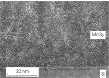
Figure 1 shows a low-magnification cross-sectional view of a MoS2 thin film deposited on Si[100],
to-gether with the corresponding diffraction pattern. The deposition temperature was 300 °C. The upper part of the film is made of lamellae perpendicular to the substrate. The density, determined by film weight and thickness measurement, is low (p ~ pbuik/3), because of the presence of voids between lamellae. Close to the interface, a thin zone, more compact, is visible. The thin white line between MoS2 and Si is native amorphous
silicon oxide.
Higher magnification reveals the connection be-tween morphology and crystalline structure (Fig. 2). Fringes corresponding to (002) planes, with ~ 6 A spac-ing, are visible on the picture. Near the interface, the dense zone is made of crystallites oriented with their (002) planes parallel with the substrate, whereas in the upper part of the film the lamellae contain crystallites having their (002) planes mostly perpendicular to the substrate. The thickness of the dense parallel zone is
equal to 5-10 times the (002) lattice plane spacing ( 3 - 6 nm). This general structure is present indepen-dently from the degree of crystallization, which itself increases with the deposition temperature.
B. First stages of growth
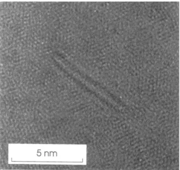
Figure 3 shows a very thin MoS2 film on Si, with
(002) lattice planes visible. Its thickness is 1-2 nm, constant over wide areas. It indicates a very fast surface covering, which can be explained by the high growth velocity in the [wvO] directions.
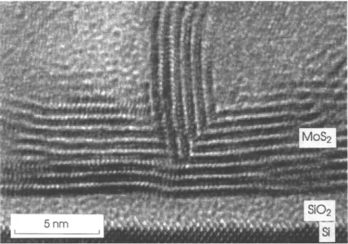
Figure 4 is a high magnification view of the interfacial region of a sample similar to those of Figs. 1 and 2. Its main features are, first, the parallel layer with the interface and, second, the root of a lamella growing from the parallel layer. The interface between silicon oxide and MoS2 is well defined. Two simple interface
models can be tested using HRTEM image calculations. In the first model, a MoS2 crystal lies on the silicon oxide
surface. The S surface being weakly reactive, the average separation between oxide surface and MoS2 has been
taken approximately equal to the distance separating two adjacent S planes in a MoS2 crystal. In the second one,
the first S plane of the MoS2 crystal has been removed,
leading to a more reactive interface between silicon oxide and a Mo plane. The distance between both phases is smaller (approximately 1 A). The amorphous silicon oxide layer itself has been modeled as a random distri-bution of Si and O atoms in cells, each one containing three SiO2 molecules. The cell volume was defined in
FIG. 1. Low magnification TEM micrograph and electron diffraction pattern of a M0S2 thin film on Si[100]. The electron beam is parallel with the interface (cross section).
FIG. 2. TEM cross-sectional micrograph of a M0S2 film on SiflOO]. The fringes correspond to M0S2 (002) planes. The amorphous zone between Si and M0S2 is silicon oxide.
FIG. 3. TEM cross-sectional micrograph of a very thin M0S2 film ( 1 - 2 nm thick). The film is completely continuous.
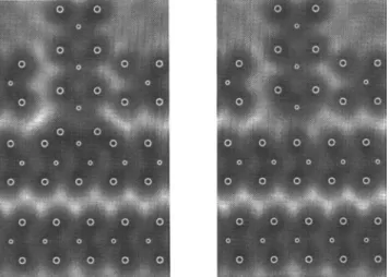
order to reproduce the density of the material. The results are shown in Fig. 5. The zone axis for MoS2 is [100],
although the general direction of observation in real cases is [uvO]. For thin samples and near the Scherzer defocus, the main features of the calculated image do not show a strong dependence on thickness and defocus. For the MoS2 crystal, bright (002) fringes with ~ 6 A
periodicity fill the empty spaces between adjacent S planes. The image details in the direction parallel with these fringes may be different in real images because of the random orientation of crystallites around their
~~c axis. In the first model, a last bright fringe fills the
empty space between MoS2 and the amorphous oxide.
Its distance from the previous one is also close to 6 A. In the second one, the fringe between the two materials is less defined, and its distance from the previous one is shorter. The first model can be recognized at many places along the interface on Fig. 4. At other sites, the aspect of the interface does not allow for a distinction between the second model and an effect of substrate roughness along the direction of observation.
C. Growth of lamellae
The crystalline orientation relationships between the lamellae in their first stages of growth and the underlying crystallites in the parallel layer can be determined using electron diffraction and HRTEM. When the film is thin enough, i.e., if the lamellae are small enough, the (002) lattice planes of the lamellae tend to be parallel with the (100) planes of the underlying parallel crystals. This is illustrated in Fig. 6, which is a high magnification detail
FIG. 4. High-resolution TEM micrograph of the interfacial region of the film of Figs. 1 and 2 (cross section). The image shows, first, the interface between silicon oxide and the first M0S2 layer, and second, the root of a lamella. White fringes correspond to M0S2 (002) planes.
FIG. 5. Computed HRTEM images corresponding to different inter-face models. Bottom: amorphous SiC>2; top: MoS2 crystal. The circles indicate atom positions.
of a MoS2 film deposited on amorphous carbon, seen
along an axis perpendicular to the interface. This result is confirmed by a statistical study on several lamellae. The electron diffraction pattern of Fig. 1 shows diffraction spots due to the Si substrate and rings corresponding to the MoS2 film. The zone axis for Si is [110]. The MoS2
• ••; •'. V r ^ & i
H~
tf
•mmm
• • - : » .:.'. • . • • • • • • " I - . " - . . '
(002) ring is separated in two parts, corresponding to the two main crystallite orientations—parallel or perpen-dicular to the substrate. The (100) ring is primarily due to lamellae having their ~~c axis parallel with the electron beam. Its inhomogeneity indicates that the cor-responding crystallites tend to have their (100) planes parallel with the interface. These orientation relation-ships are summarized in Table I. Figure 7 is a schematic model of the local situation. The exact position of the lamella is arbitrary. The two crystals show a lattice coincidence, with a periodicity a0, along a common
[100]. This suggests the presence of a chemical bond-ing along a contact line parallel with this direction. Observation of well-crystallized films shows the occur-rence of this branching mechanism also in the bulk of the film, leading to complex dendritic-like structures (Fig. 8).
Information about the structure at the basis of the lamellae can be extracted from the fringe pattern of Fig. 4. At the root of the lamella, the horizontal white fringe is interrupted. Image calculations show that it can be due to a filling of the empty space between S planes. Two simplified models are shown on Fig. 9 with the corresponding calculated fringe pattern. They do not pretend to give an exact atom position or to be chemically realistic. Neither do they take into account the presence of impurities. The S surfaces being weakly reactive, the first model considers a lamella bonded to the parallel layer through interaction with a Mo plane. It was arbitrarily decided to replace an array of S atoms in a [100] direction by the Mo atoms of the lamella. In the second model, there is an empty space above the S surface. The lamella is not strongly bonded to the underlying crystal. The fringe pattern of model one is similar, in its main features, to the experimental image. Furthermore, this model, with a lamella bonded along a line, is consistent with the matching of the interatomic spacings in both crystals along the bond-ing line.
D. Influence of partial H2O pressure
Films have been deposited in the presence of vari-able amounts of H2O vapor in the chamber atmosphere.
TABLE I. Relative crystalline orientations in the branching process.
(002) (002) (100) B (002) (100) (002) FIG. 6. High-resolution TEM micrograph of a very thin M0S2 film
showing the early growth of a lamella. The electron beam is perpen-dicular to the interface (top view).
A: Old crystal. B: New crystal.
c/4
FIG. 7. Schematic model of the crystalline orientations in the branching process. The exact relative positions of both crystals are arbitrary.
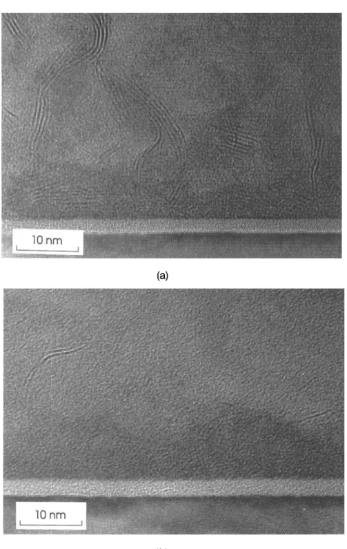
For H2O pressures up to 5 • 10~3 Pa, the film structure
does not show any changes; the interface remains well
crystallized. With 1.3 • 10"2 Pa H2O, a partial
amor-phization of the interfacial region occurs (Fig. 10). With 5 • 1(T2 Pa H2O, a dense, amorphous region extends
from the interface over 40 nm. Subsequent crystal-lization occurs gradually, leading to randomly oriented crystallites. Those oriented with [MVO] directions perpendicular to the substrate can grow without obstacles and lead to the lamellar structure in the outer part of the film. At H2O pressures higher than 10"1 Pa, the films
are completely amorphous.
E. Annealed films
The structure of MoS2 thin films is strongly
related to the growth mechanisms. High-temperature grown films can be compared with films deposited at low temperature and low power and annealed under vacuum at 500 °C for 1 h. Before annealing, these
FIG. 8. Cross-sectional TEM micrograph of M0S2 crystals in the bulk of the film, showing the dendritic-like structure induced by the branching processes.
FIG. 9. Computed HRTEM images of the root of a lamella, from two different models (see Fig. 4). The circles indicate atom positions.
iOnm
• • • • . - . . . : : • : • , : • !
(a)
10 nm
(b)
FIG. 10. Cross-sectional TEM micrograph of the interface of MoS2thin films contaminated during deposition by different amounts of water vapor: (a) 1.3 • 10"2 Pa and (b) 5.3 • 10"2 Pa.
films were shown to be amorphous by x-ray diffraction measurements. The structure after annealing is shown in Fig. 11. No lamellar structure is apparent. Crystallites are randomly oriented in the whole film, even at the interface. The interface is rougher than in films deposited at 500 °C, where the presence of the inert S layer inhibits the thermally activated diffusion or chemical reaction at the interface. In the case of an amorphous film such
phenomena are allowed by the presence of dangling bonds near the interface.
IV. CONCLUSION
The structure of sputtered MoS2 thin films is strongly
related to the growth and crystallization mechanisms. For films deposited under pure argon and high substrate
FIG. 11. Cross-sectional TEM micrograph of an originally amor-phous MoS2 thin film after 1 h annealing under vacuum at 500 °C.
temperature, the films are crystallized. The crystallites at the interface have their (002) planes parallel with the substrate. They form a uniform coverage, a few nano-meters thick. Crystal growth is characterized by branch-ing processes with epitaxial characteristics. Occurrbranch-ing during the growth of the parallel layer near the interface, this process leads to the growth of crystallites having their (002) planes perpendicular to the substrate. If the degree of crystallization is high enough, i.e., if the length of crystallites is of the same order of magnitude as the film thickness, the lamellar morphology appears, charac-terized by the presence of vertical flakes. Branching can be observed also from crystallites in the bulk of the film, as described by Buck7 under the term "dendritic growth".
This kind of structure has been observed for all substrate temperatures, provided that they were high enough for the film to be crystallized. Water contamination during deposition leads to films with an amorphous interface. Crystallization occurs during the subsequent stages of
growth in an isotropic way. The final lamellar morphol-ogy of these films is the result of a geometrical selection mechanism. The crystals having their growth directions [MVO] perpendicular to the substrate grow without obsta-cles, whereas the growth of differently oriented crystals is limited. The annealing of amorphous films leads to an isotropic crystallization in the whole thickness without lamellar morphology, and to a diffused interface.
To conclude, we can point out that, besides the geo-metrical description of the growth phenomena present in this paper, an alternative approach might consist of an explanation based on energetic or thermodynamic arguments.
ACKNOWLEDGMENTS
This work has been financially supported by the Fondation Suisse pour la Recherche en Microtechnique and by the Fonds National Suisse de la Recherche Scientifique.
REFERENCES
1. R. Bichsel, P. Buffat, and F. Levy, J. Phys. D: Appl. Phys. 19, 1575-1585 (1986).
2. J.R. Lince and P.D. Fleischauer, J. Mater. Res. 2, 827-838 (1987).
3. V. Buck, Wear 91, 281-288 (1983).
4. A. Aubert, J. P. Nabot, J. Ernoult, and Ph. Renaux, Proc. 7th Int.
Conf. on Ion and Plasma Assisted Techniques, 281-286 (1989).
5. V. Buck, Thin Solid Films 139, 157-168 (1986). 6. V. Buck, Vacuum 36, 89-94 (1986).
7. V. Buck, Wear 114, 263-274 (1987).
8. P. A. Bertrand, J. Mater. Res. 4, 180-184 (1989). 9. P.D. Fleischauer, ASLE Trans. 27 (1), 82-88 (1983).
10. S. Kikkawa, M. Miyazaki, and M. Koizumi, J. Mater. Res. 5, 2894-2901 (1990).
11. J. Moser, H. Liao, and F. Levy, J. Phys. D: Appl. Phys. 23, 624-626 (1990).
12. P. A. Stadelmann, Ultramicroscopy 21, 131-146 (1987). 13. P. Goodman and A. F. Moodie, Acta Cryst. A30, 280-290 (1974).
![Figure 1 shows a low-magnification cross-sectional view of a MoS 2 thin film deposited on Si[100], to-gether with the corresponding diffraction pattern](https://thumb-eu.123doks.com/thumbv2/123doknet/14910617.658323/2.864.62.798.704.1073/figure-magnification-sectional-deposited-gether-corresponding-diffraction-pattern.webp)