HAL Id: tel-01283931
https://tel.archives-ouvertes.fr/tel-01283931
Submitted on 7 Mar 2016
HAL is a multi-disciplinary open access
archive for the deposit and dissemination of sci-entific research documents, whether they are pub-lished or not. The documents may come from teaching and research institutions in France or abroad, or from public or private research centers.
L’archive ouverte pluridisciplinaire HAL, est destinée au dépôt et à la diffusion de documents scientifiques de niveau recherche, publiés ou non, émanant des établissements d’enseignement et de recherche français ou étrangers, des laboratoires publics ou privés.
Enhancement of nonlinear effects using silicon plasmonic
structures
Jihua Zhang
To cite this version:
Jihua Zhang. Enhancement of nonlinear effects using silicon plasmonic structures. Optics [physics.optics]. Université Paris Saclay (COmUE); Université Huazhong des Sciences et Technologies (Wuhan, Chine), 2015. English. �NNT : 2015SACLS171�. �tel-01283931�
THESE DE DOCTORAT
DE L’UNIVERSITE PARIS-SACLAY,
préparée à l’Université Paris-Sud
ÉCOLE DOCTORALE N°575
Electrical, Optical, Bio – physics and Engineering (EOBE)
Spécialité de doctorat : Physique
Par
M. Jihua ZHANG
Enhancement of nonlinear effects using
silicon plasmonic structures
Thèse présentée et soutenue à Orsay, le 02 décembre 2015 : Composition du Jury :
M. Guillaume Bachelier, Maître de conférences HDR, Université Joseph Fourier, Rapporteur
M. Gilles Renversez, Professeur, Université d'Aix-Marseille, Rapporteur M. Alexandre Bouhelier, DR-CNRS, Université Bourgogne Franche-Comté, Examinatrice
Mme. Béatrice Dagens, DR-CNRS, Université Paris-Sud, Examinateur M. Eric Cassan, Professeur, Université Paris-Sud, Directeur de thèse
Président du jury -Numéro de NNT : 2015SACLS171
Titre : Structures plasmoniques pour le renforcement des effets nonlinaires et
la réalisation de fonctions tout-optiques en photoniques sur silicium
Mots clés :
Photonique silicium, plasmonique, optique nonlinéaireRésumé :
L’augmentation des flux d’information sur puce conduit l’électronique intégrée à un certain nombre de limitations, liées en particulier à la saturation des débits binaires transmissibles entre blocs et cœurs et au niveau excessif de puissance dissipée. Dans ce contexte, la photonique silicium a été proposée il y a plusieurs années comme une solution intéressante pour lever certains verrous. Ce domaine, qui a connu un intérêt marqué depuis, repose sur le développement de liens optiques sur puce, donc sur le développement de toutes les structures nécessaires pour l’émission, le guidage, la modulation, et la détection des signaux optiques. Au stade actuel, les progrès ont été spectaculaires mais des difficultés demeurent : d’une part, la puissance consommée par les composants optoélectroniques, en particulier de modulation, se situe toujours au-dessus des niveaux requis par les applications ; d’autre part, la taille des composants optiques intégrées classiques ne peut pas être miniaturisée en-dessous de la limite de diffraction (de l’ordre de 250nm dans les cas usuels de la photonique silicium, dans la fenêtre des longueurs d’onde télécoms λ=1,55µm), ce qui ne permet pas d’envisager une co-intégration poussée de l’optique avec l’électronique CMOS.
Dans cette thèse, nous avons exploré les potentialités de l’utilisation de matériaux organiques non-linéaires au sein de structures métalliques pour la réalisation de guides d’ondes plasmoniques nonlinéaires. Les propriétés de la plasmonique autorisant la réalisation de structures sub-longueur d’onde à confinement extrême du champ électromagnétique, les composants qui en découlent sont caractérisés par un renforcement significatif des effets optiques non-linéaires et leur co-intégration avec l’électronique devient envisageable en terme de compacité et d’encombrement.
Nous avons développé une approche basée sur la théorie des modes couplées applicable à des guides à pertes (absorption par les métaux) et, couplées à des calculs par éléments finis, nous l’avons appliquée à l’exploration des plusieurs effets. Deux types de guides ont été considérés, guides plasmoniques et guides plasmoniques hybrides. Les phénomènes de génération de seconde harmonique et de rectification optique (assistée électriquement ou pas) ont été étudiés principalement ; les compromis entre pertes de propagation (par absorption) et confinement du champ électromagnétique ont été explorés et l’ensemble a conduit à proposer plusieurs configurations caractérisées par des longueurs d’interaction de quelques dizaines de µm typiquement et des efficacités (de conversion de longueur d’onde, de rectification, etc) se situant au-delà de l’état de l’art actuel.
Ces propositions théoriques ont été complétées par un volet expérimental, concrétisé par la fabrication de structures plasmoniques, et qui a permis de valider la possibilité d’une injection efficace de la lumière depuis une fibre optique vers des guides plasmoniques très sub-longueur d’onde.
iii
Acknowledgement
First, I would like to thank my supervisors Prof. Eric Cassan and Prof. Xinliang Zhang for providing me with the opportunity to complete my joint PhD thesis at University Paris-Sud and Huazhong University of Science and Technology. Prof. Eric Cassan is the most easy-going professor I have even seen. He always amazes me with his endless energy, passion, and knowledge. Prof. Xinliang Zhang has been supportive and has given me the freedom to pursue various directions without objection. They were and remains my best role model for a scientist, mentor, and teacher.
I would also like to thank my committee members, Prof. Guillaume Bachelier. Prof. Gilles Renversez, Prof. Alexandre Bouhelier and Prof. Béatrice Dagens for serving as my committee members. Thank you for letting my defense be an enjoyable moment, and for your brilliant comments and suggestions.
I am also very grateful to all the professors in the two labs Prof. Laurent Vivien, Prof. Delphine Marris-Morini, Prof. Jianji Dong, Prof. Yu Yu and Prof. Lei Shi for their help, scientific advice and insightful discussions. I want to thank present and past group members for the good atmosphere they have built in the lab and good time we have shared together. Thanks to Ping Zhao and Yuan Yu for helping me get used to the graduate life and for sharing their knowledge.
A special thanks to my family for their unconditional support and love. Words cannot express how grateful I am to my mother ShuZhen Zhang, my father Shiyun Zhang and my brother Jixin Zhang for all of the sacrifices that they have made for me. I also want to thank my girlfriend Mengwan Lv for her faith, support and love.
Jihua Zhang December 2015
iv
Abstract
With the rapid increasing bandwidth of data transmission and signal processing, integrated electronics encounters strong challenges due to its intrinsic bandwidth bottleneck and large power consumption at high data rate. Silicon photonics provides a low-cost solution to overcome these challenges by replacing some parts of the original electronic integrated circuits with photonic integrated circuits. After a decade of development, silicon photonics is now the most active discipline and most promising platform within the field of integrated optics. However, in the process of further development, new stumbling blocks emerge. The sizes of photonic devices are restricted by the diffraction limit and thus result in a strong mismatch between photonic and electronic components in their co-integration. In addition, lack of second-order nonlinearity and existence of free carrier effects in silicon tend to limit the versatility and operating speed of nonlinear optical signal processing, which plays a key role in multiple photonic functionalities.
Plasmonics is a good candidate to overcome the first obstacle due to its ability to confine the optical field into nanoscale beyond the diffraction limit. Moreover, the localized strong field enhancement in plasmonic structures enhances interaction of light and matter, which is promising for enhancing the efficiency and reducing the power consumption in nonlinear applications. For the second limit, organic materials with large nonlinear susceptibility and free of carrier effects have attracted a growing attention in the last years and their integration on silicon have been proposed to be an efficient silicon organic hybrid platform.
In this dissertation, we combine the plasmonic and organic technologies onto the silicon photonics platform to investigate silicon plasmonic organic structures and explore the nonlinear effects induced in them. Silicon plasmonic organic structures, which combine the advantages of silicon with the ultra-compact and strong-field
v
materials, have great potentials for nonlinear integrated optics.
A full-vectorial nonlinear coupled-wave equation model valid for lossy plasmonic waveguides is proposed and then used to analyze nonlinear effects in silicon plasmonic waveguides. This dissertation addresses the use of two kinds of plasmonic waveguides: plasmonic slot waveguides (PSW) and hybrid plasmonic waveguides (HPW).
Specifically, an enhanced second harmonic generation (SHG) is proposed in the PSW. A normalized efficiency up to 105 W-1cm-2 is predicted, which is four orders of magnitude higher than those previously reported. Then, by applying two electrodes onto the two sides of PSW, the SHG process can be controlled by the voltage, which is proposed to be a new mechanism for high-speed electro-optic modulation. Another nonlinear effect investigated in PSW is the optical rectification (OR) effect, through which an electrical signal is generated between the two metal slabs when an intensity modulated optical signal is injected into the PSW. This efficient OR process supports flat response for a wide range of wavelength, which can be applied for the realization of high-speed broadband optical detection and demodulation.
The enhanced mid-to-near-infrared SHG in HPW is also explored. The SHG yield is as large as 8.8% for a pumping power of 100 mW and a short length of 120 μm. Then, by utilizing the resonant effect in a microring, the efficiency is further enhanced by two orders of magnitude. This provides a potential route for realizing efficient frequency conversion between mid-infrared and near-infrared wavebands on a chip. Besides, efficient optical parameter amplification (OPA) is also studied in a symmetric HPW. Based on the OPA, phase regeneration of phase-shift keying signals is then theoretically proposed.
The design, fabrication and measurement of PSWs are also described. The fabricated PSW have good performance in terms of loss. By spin-coating the commercial available second order nonlinear polymer, the nonlinear response of the PSW is under testing at the present writing time.
vi
Contents
Acknowledgement iii
Abstract iv
List of Figures ix
List of Tables xiii
List of Publications xiv
List of Abbreviations xvii
1 Introduction 1
1.1 Silicon photonics: opportunities and challenges ... 2
1.2 Plasmonics: fundamental and applications ... 8
1.3 Nonlinear silicon plasmonics ... 14
1.4 Organization ... 17
2 Theoretical analysis of nonlinear processes in silicon plasmonic waveguides 19 2.1 Silicon plasmonic waveguides ... 19
2.1.1 Plasmonic slot waveguides ... 23
2.1.2 Hybrid plasmonic waveguide ... 25
2.2 Nonlinear coupled-wave equations ... 29
2.2.1 Derivation ... 29
2.2.2 Principles to enhance nonlinear effects ... 34
vii
3.1 Enhanced second harmonic generation in plasmonic slot waveguides ... 45
3.1.1 Introduction ... 45
3.1.2 Waveguide structure and nonlinear modeling approach ... 47
3.1.3 Enhanced SHG in the proposed plasmonic slot waveguide ... 52
3.1.4 Further improvement of SHG efficiency by tailoring the waveguide asymmetry ... 54
3.1.5 Conclusion ... 58
3.2 High-speed electro-optical modulator based on electrically controlled second harmonic generation ... 58
3.2.1 Introduction ... 58
3.2.2 Waveguide structure and nonlinear modeling approach ... 60
3.2.3 Effectively controlled SHG by voltage ... 63
3.2.4 Discussion and conclusion ... 66
3.3 Broadband high-speed optical detection based on the optical rectification effect ... 67
3.3.1 Introduction ... 67
3.3.2 Waveguide structure and nonlinear modeling approach ... 70
3.3.3 Effective optical rectification in plasmonic slot waveguides ... 74
3.3.4 Conclusion ... 80
3.4 Chapter summary ... 81
4 Enhancement of nonlinear effects using hybrid plasmonic waveguides 83 4.1 Enhanced second harmonic generation in hybrid plasmonic waveguides .... 84
4.1.1 Introduction ... 84
4.1.2 Waveguide structure and mode analysis ... 85
4.1.3 Efficient SHG in the proposed hybrid plasmonic waveguide ... 88
4.1.4 Conclusion ... 91 4.2 Further enhancement of second harmonic generation with microring
viii
resonators ... 91
4.2.1 Microring structure and design ... 91
4.2.2 Nonlinear model approach ... 95
4.2.3 Enhanced second harmonic generation in microring resonators ... 99
4.2.4 Conclusion ... 103
4.3 Phase regeneration of phase shift keying signals in hybrid plasmonic waveguides ... 104
4.3.1 Introduction ... 104
4.3.2 Waveguide structure and efficient optical parametric amplification ... 105
4.3.3 Proposal for phase regeneration ... 109
4.3.4 Conclusion ... 110
4.4 Chapter summary ... 110
5 Progress towards experimental nonlinear plasmonic waveguides 112 5.1 Design and optimization of waveguides and coupling tapers ... 112
5.2 Fabrication... 117
5.3 Measurement and results ... 121
5.4 Chapter summary ... 125
6 Conclusion and future steps 126 Appendix 131 Numerical method to analyze nonlinear effects... 131
ix
List of Figures
1.1 Global IP traffic growth prediction ... 1
1.2 Broadband octave-spanning frequency comb in a silicon wire waveguide ... 3
1.3 Development of chip complexity for the InP monolithic integration, hybrid silicon platform and silicon photonics ... 5
1.4 Operating speed and critical device dimension of semiconductor electronics, dielectric photonics and metallic nanoplasmonics ... 5
1.5 High-speed plasmonic phase modulator ... 8
1.6 Surface plasmon polaritons at a metal-dielectric interface ... 9
1.7 Dispersion relation of SPPs at a metal-dielectric interface ... 11
1.8 Characteristic lengths of SPP wave at the silver-air interface ... 13
1.9 Efficient third harmonic generation in a silicon-based plasmonic waveguide . 16 2.1 Structure and mode profiles of metal nanowire waveguides, metal nanoparticle chain waveguides and channel plasmon waveguides ... 21
2.2 Structure and mode profile of long range plasmonic waveguide ... 21
2.3 Structure and mode profiles of plasmonic slot waveguides, hybrid plasmonic waveguides and dielectric loaded plasmonic waveguides ... 22
2.4 Typical configuration and field distribution of the fundamental mode of a plasmonic slot waveguide ... 23
2.5 Mode properties of PSW as a function of the waveguide size ... 24
2.6 Typical configuration and field distribution of the fundamental mode of a hybrid plasmonic waveguide ... 26
2.7 Mode properties of HPW as a function of the waveguide size... 27
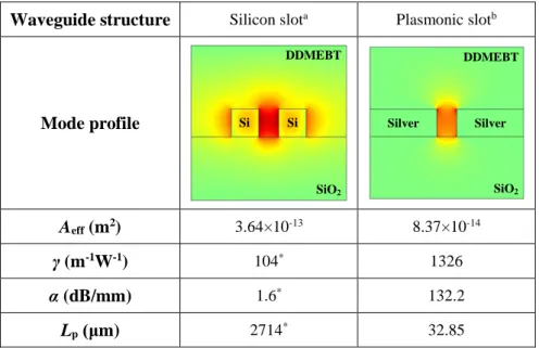
2.8 Kerr nonlinearity in silicon slot waveguide and plasmonic slot waveguide .... 41
3.1 Plasmonic slot waveguide with χ(2) polymer infiltrating into the slot ... 48 3.2 Design of the PSW with SiO2 substrate for satisfying the phase-matching
x
condition ... 51
3.3 Optical power variations of the SHG along the propagation distance ... 52
3.4 SHG properties as a function of the waveguide size ... 53
3.5 Design of the PSW with Si3N4 substrate for satisfying the PMC ... 55
3.6 Optical power variations of the SHG along the propagation distance in PSW with Si3N4 substrate ... 55
3.7 Normalized Ex distribution on the center line of the slot for the case of SiO2 substrate and Si3N4 substrate ... 56
3.8 SHG properties as a function of the pump power ... 57
3.9 Active PSW with control voltage between two sides ... 61
3.10 Power variations of FF and SH along propagation for Vc=10 V and different voltages when the polymer is centro-symmetric ... 63
3.11 Power and phase variations of FF and SH along propagation for Vc=10 V when the polymer is noncentro-symmetric ... 64
3.12 The output power and phase of SH for noncentro-symmetric case as a function of the control voltage ... 64
3.13 The normalized change of the output power of SH as a function of the control voltage ... 65
3.14 Schematic of the PSW for investigating the optical rectification effect ... 70
3.15 Electric field distributions at optical frequency and RF in the PSW ... 74
3.16 OR properties as a function of the slot height for different widths ... 75
3.17 OR properties as a function of the PSW length for different slot widths ... 76
3.18 Normalized OR efficiency as functions of the PSW geometrical size ... 76
3.19 OR properties as a function of the optical wavelength ... 78
3.20 OR properties as a function of the radio frequency ... 79
3.21 OR properties as a function of the control DC voltage ... 79
4.1 Schematic of the nonlinear hybrid plasmonic waveguide ... 86 Mode refractive indices as a function of the width and mode profiles at the phase
xi
matching point ... 87
4.3 Ey distributions on the center line along y-direction for different modes ... 88
4.4 Intensity variations in the propagation with pump power of 100 mW ... 89
4.5 Phase mismatch as functions of width and wavelength of FF ... 90
4.6 Schematic of the silicon-organic hybrid plasmonic microring resonator ... 92
4.7 Δn = nSH - nFF as functions of the radius and width of the bend waveguide .... 93
4.8 neffkFFR and loss of a 90˚ bend at the phase matching line as functions of the radius ... 93
4.9 Ez distributions for the phase-matched modes at FF and SH ... 94
4.10 Schematic of second harmonic generation in a single pass MRR ... 96
4.11 Analytic solution and numerical solution of the SHG efficiency as functions of the propagation length in HPW ... 99
4.12 SHG efficiency as functions of the transmission coefficients ... 100
4.13 SHG properties as a function of the gap ... 101
4.14 Transmission spectra of the 3D MRR structure ... 102
4.15 SHG efficiency as a function of the attenuation coefficients ... 103
4.16 Schematic diagram of the proposed symmetric HPW ... 105
4.17 Intensity and phase evolutions in the propagation when φs(0) = 0 ... 107
4.18 Intensity and phase evolutions in the propagation when φs(0) = 0.2π, 0.8π .. 108
4.19 Gain and output phase of SW versus the φs(0) when L = 150 µm... 108
5.1 Schematics of the fabricated PSW and taper couplers ... 113
5.2 OR properties as a function of the slot height for different widths ... 114
5.3 OR properties as a function of the PSW length for different slot widths ... 114
5.4 Transmittance of the PSW with two taper couplers for different taper sizes . 116 5.5 Fabrication procedures of the nonlinear plasmonic slot waveguide ... 117
5.6 Metallographic microscope pictures in the fabrication ... 118
5.7 SEM pictures of silicon stripe waveguide and grating couplers ... 119
xii
5.9 SEM pictures of fabricated PSWs with different widths ... 120
5.10 SEM pictures of fabricated PSWs with different lengths ... 120
5.11 Experimental setup to measure the fabricated waveguides ... 121
5.12 Experimental measured loss of PSW with different lengths ... 122
5.13 Poling condition of the M1 polymer ... 124
5.14 Diagram of the electrodes contact for the PSW in the poling process and measurement ... 124
xiii
List of Tables
2.1 Electrooptic coefficients for various second order nonlinear materials ... 36 2.2 Nonlinear coefficients for various third order nonlinear materials ... 36 2.3 Comparison of Kerr nonlinearity in silicon slot waveguide and plasmonic slot waveguide ... 41
3.1 The optimized height and length for different widths and the corresponding OR results ... 77
xiv
List of Publications
Journals
1. H. L. Zhou, J. J. Dong, Y. F. Zhou, J. H. Zhang, M. Liu, X. L. Zhang, "Designing Appointed and Multiple Focuses With Plasmonic Vortex Lenses, " Photonics Journal, IEEE 7(4) 1-7 (2015).
2. H. L. Zhou, Y. F. Zhou, J. H. Zhang, and J. J. Dong, "Double-Slit and Square-Slit Interferences With Surface Plasmon Polaritons Modulated by Orbital Angular Momentum Beams," Photonics Journal, IEEE 7(2), 1-7 (2015).
3. Z. Q. Wang, L. Shi, X. B. Xu, J. H. Zhang, J. L. Zhang, and X. L. Zhang, "Optical nonreciprocity with large bandwidth in asymmetric hybrid slot waveguide coupler," Optics Express 23 (3), 3690-3698 (2015).
4. K. S. Chen, J. Hou, Z. Y. Huang, T. Cao, J. H. Zhang, Y. Yu, and X. L. Zhang, "All-optical 1st- and 2nd-order differential equation solvers with large tuning ranges using Fabry-Pérot semiconductor optical amplifiers," Optics Express 23(3), 3784-3794 (2015).
5. J. H. Zhang, L. Shi, Y. L. Wang, E. Cassan, and X. L. Zhang, "On-chip high-speed optical detection based on an optical rectification scheme in silicon plasmonic platform," Optics Express 22(22), 27504-27514 (2014).
6. J. H. Zhang, E. Cassan, and X. L. Zhang, "Enhanced mid-to-near-infrared second harmonic generation in silicon plasmonic microring resonators with low pump power," Photonics Research 2(5), 143-149 (2014).
7. J. H. Zhang, E. Cassan, and X. L. Zhang, "Electrically controlled second-harmonic generation in silicon-compatible plasmonic slot waveguides: a new modulation scheme," Optics Letters 39(13), 4001-4004 (2014).
xv
8. J. H. Zhang, E. Cassan, and X. L. Zhang, "Wideband and Compact TE-Pass/TM-Stop Polarizer Based on a Hybrid Plasmonic Bragg Grating for Silicon Photonics," Lightwave Technology, Journal of 32(7), 1383-1386 (2014).
9. J. H. Zhang, E. Cassan, and X. L. Zhang, "Efficient second harmonic generation from mid-infrared to near-infrared regions in silicon-organic hybrid plasmonic waveguides with small fabrication-error sensitivity and a large bandwidth," Optics Letters 38(12), 2089-2091 (2013).
10. J. H. Zhang, P. Zhao, E. Cassan, and X. L. Zhang, "Phase regeneration of phase-shift keying signals in highly nonlinear hybrid plasmonic waveguides," Optics Letters 38(6), 848-850 (2013).
11. J. H. Zhang, E. Cassan, D. S. Gao, and X. L. Zhang, "Highly efficient phase-matched second harmonic generation using an asymmetric plasmonic slot waveguide configuration in hybrid polymer-silicon photonics," Optics Express 21(12), 14876-14887 (2013).
12. P. Zhao, J. H. Zhang, Y. Yu, J. J. Dong, L. Shi, Y. Liu, and X. L. Zhang, “In-line polarization-dependent microfiber interferometers and their applications in UWB signal generation,” Optics Express 21(7), 8231-8239 (2013).
13. P. Zhao, J. H. Zhang, G. H. Wang, M. Jiang, P. P. Shum, X. L. Zhang, “Longitudinal coupling effect in microfiber Bragg gratings,” Optics Communications 285(23), 4655-4659 (2012).
14. P. Zhao, Y. H. Li, J. H. Zhang, L. Shi, and X. L. Zhang, “Nanohole induced microfiber Bragg gratings,” Optics Express 20(27), 28625-28630 (2012).
Conferences
1. J. H. Zhang, E. Cassan, and X. L. Zhang, “Enhanced mid-to-near-infrared second harmonic generation in silicon-organic hybrid plasmonic microring resonators,”
xvi
Conference on Lasers and Electro-Optics (CLEO) 2014, Paper: JTh2A.46.
2. J. H. Zhang, X. L. Zhang, and E. Cassan, "High-yield second-harmonic generation from mid-infrared to near-infrared regions in silicon-organic hybrid plasmonic waveguides," in Proc. SPIE 9136, Nonlinear Optics and Its Applications VIII and Quantum Optics III (Brussels, 2014), pp. 91360D-91360D-6.
3. J. H. Zhang, E. Cassan, and X. L. Zhang, “Efficient mid-to-near-infrared second harmonic generation based on silicon-organic hybrid plasmonic waveguides,” Asia Communications and Photonics Conference and Exhibition (ACP) 2013, Paper: 1752414.
4. J. H. Zhang, P. Zhao, E. Cassan, and X. L. Zhang, “Proposal for phase regeneration of phase-shift keying signals in nonlinear hybrid plasmonic waveguides,” International Photonics and OptoElectronics Meetings (POEM) N3 2013, Paper: NSu1B.4.
5. P. Zhao, J. H. Zhang, Z. Wu, and X. L. Zhang, “Model of Bragg grating written in subwavelength-diameter fiber taper,” Asia Communications and Photonics Conference and Exhibition (ACP) 2011, Paper: 830720.
xvii
List of Abbreviations
AC Alternating current
CMOS Complementary metal-oxide semiconductor CSHG Conventional second harmonic generation
CW Continuous wave
DC Direct current
EBE Electron beam evaporation EBL Electron beam lithography
ECSHG Electrically controlled second harmonic generation EFISHG Electrical field induced second harmonic generation
EO Electro-optic
FCA Free carrier absorption FCD Free carrier dispersion FDTD Finite different time domain
FF Fundamental frequency
FWM Four wave mixing
HPW Hybrid plasmonic waveguide
ICPRIE Inductively coupled plasma reactive ion etching LRSPP Long-range surface plasmon polariton
MIR Mid-infrared
MPM Mode phase matching
MRR Microring resonator MSM Metal-silicon-metal
NCC Nonlinear coupling coefficient NCE Nonlinear coupled-wave equation
NIR Near-infrared
xviii
OF Optical frequency
OPA Optical parameter amplification OR Optical rectification
ORPD Optical rectification based photodetector PECVD Plasma enhanced chemical vapor deposition PMC Phase matching condition
POH Plasmonic organic hybrid PSK Phase shift keying
PSW Plasmonic slot waveguide
PW Pump wavelength
QPM Quasi phase matching
RF Radio frequency
RI Refractive index
SEM scanning electron microscope SHF Second harmonic frequency SHG Second harmonic generation
SHPW Symmetric hybrid plasmonic waveguide SOH Silicon organic hybrid
SOHPMR Silicon-organic hybrid plasmonic microring resonator SOI Silicon-on-insulator
SOPHW Silicon-organic hybrid plasmonic waveguide
SP Surface plasmon
SPD Semiconductor photodetector SPP Surface plasmon polariton SSW Silicon slot waveguide
SW Signal wavelength
TM Transverse magnetic
Chapter 1
Introduction
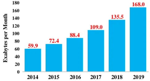
Today, with the rapid development of information technologies, the capacity of global internet is becoming larger and larger. According to the Cisco Visual Networking Index Global Forecast, global IP traffic has increased fivefold over the past five years, and will increase threefold over the next five years. As shown in Fig. 1.1, overall IP traffic is expected to grow to 168 exabytes per month by 2019, up from 59.9 exabytes per month in 2014. This ever-increasing bandwidth requires exponential increases in communication bandwidth at all levels of the system and becomes a big challenge to the conventional electronic circuits due to its intrinsic bandwidth bottleneck and large power consumption at high data rate. At high bit rates of 10 Gbits/s and higher, the circuit’s alternating current characteristics begin to dominate the impedance, inductance, and conductance of the electric line, severely distorting the signal. Meanwhile, electric signal attenuation and power dissipation rise dramatically with higher data rate. To deal with the increasing bandwidth requirement of future data communication networks, optical circuits have been widely accepted as a viable alternative owing to their strengths such as low loss and near infinite optical bandwidth.
E x a b y te s p er M o n th 0 20 40 60 80 100 120 140 160 180 2014 2015 2016 2017 2018 2019 59.9 72.4 88.4 109.0 135.5 168.0
Fig. 1.1 Global IP traffic growth prediction. Figure taken from: Cisco Visual Networking Index Global Traffic Forecast, 2014-2019.
1.1 Silicon photonics: opportunities and challenges
At present, the fiber based long haul transmission of optical signals is very mature. Optical connecting between computers with fibers is also commercial. By employing the wavelength division multiplexing and spatial division multiplexing techniques, the gross transmission throughput of 255 Tbit/s has been demonstrated in a single few-mode multicore fibre [1]. This fact of high bandwidth in a single fiber is not enough, the same has to be done at the chip scale. This relates to another aspect of photonics: the integrated photonics field that deals with on-chip and chip-to-chip optical interconnections and signal processing. In this respect, silicon photonics has drawn a lot of attention in the last decade and has been regarded as the most promising platform in integrated photonics. Motivations to develop silicon photonics include [2-8]:
The high-quality of silicon-on-insulator (SOI) wafers, which are an ideal platform for creating planar waveguide circuits. The strong optical confinement offered by the high index contrast between silicon (n = 3.45) and SiO2 (n = 1.45) in the near-infrared region makes it possible to scale photonic devices to the hundreds of nanometers level;
Silicon is a transparent material for the wide wavelength band from 1100 nm to 7000 nm approximately, which is far from being limited to the near-infrared communication window of around 1550 nm;
Silicon has excellent material properties that are important in photonic devices. These include high thermal conductivity (∼10× higher than GaAs), high optical damage threshold (∼10× higher than GaAs), and high third-order optical nonlinearities;
Today’s mature complementary metal-oxide semiconductor (CMOS) techniques could also allow low-cost, large-scale manufacturing for silicon photonic devices.
on ultrafast nonlinear optical signal processing have been theoretically proposed or experimentally demonstrated [9, 10]. For example, R. Salem et al. reported the signal regeneration by using four-wave mixing on silicon chip [11]. Recently, B. Kuyken et al. demonstrated an octave-spanning frequency comb spanning from the telecom wavelength window ~1500 nm to the mid-infrared wavelength range at 3300 nm in a silicon nanophotonic wire waveguide [12]. As shown in Fig. 1.2, by designing the air-clad photonic wire with a rectangular cross-section of 1600 nm × 390 nm and slightly over etching by 10nm into the buried oxide, the silicon wire has nonlinear parameter of 38 W-1m-1 at 2300 nm. The zero-dispersion wavelength is at 2180 nm and the dispersion remains low over a wide spectral band. The spectra at the input from an optical parametric oscillator and output of the waveguide are shown in Fig. 1.2(c) for a pulse energy of 16 pJ. The spectrum of the pulses is significantly broadened in the silicon photonic wire waveguide through self-phase modulation.
(a) (b)
(c)
Fig. 1.2 (a) The simulated dispersion of the photonic wire waveguide. The zero-dispersion wavelength of the quasi-TE mode is at 2180 nm, while the dispersion is normal at shorter wavelengths and anomalous at longer wavelengths. The waveguide cross-section is shown
in the inset. (b) Experimental set-up: the optical parametric oscillator pumped by a Ti-Sapphire mode-locked laser is coupled to the silicon chip with a lens. The output of the chip can be sent to a photodetector or a spectrometer. (c) The spectrum at the input (red) and the output (black) of the silicon nanowire. Figure taken from ref. [12].
However, in the way to realize chip-scale integrated optical interconnects with low power consumption, advanced functionality and good convergence with electronics, two stumbling blocks emerge in silicon. Firstly, as we know, one of the key advantages of silicon photonics is that photonic and electronic functions can be integrated and fabricated onto the same chip. Nevertheless, the sizes of photonic devices are limited by the diffraction limit, which means that the dimension cannot be smaller than the half wavelength in the dielectric (D ≥ λ/2n). As a result, there exists a size mismatch between photonic and electronic components in their co-integration. Secondly, the lack of second-order optical nonlinearity and the existence of free carrier effect limit the versatility and operating speed of nonlinear silicon photonics, which plays a key role in combining multiple new optical functionalities with electronics on a single chip [9].
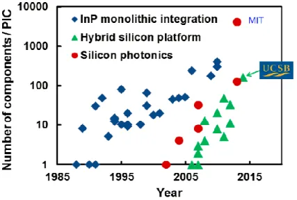
As we know in integrated electronics, there is a clear exponential development in the number of transistors per chip, which has been doubling every two years on average during the last four decades. This phenomenon is known as the Moore’s law [13]. Similarly, the development of integrated photonics is also considered to obey a photonic Moore’s law. The component count on a single chip becomes larger and larger with time [7, 14]. For example, Fig. 1.3 shows the complexity development of three mainstream integrated photonic platforms measured as the number of components integrated on a single chip [7]. However, the ultimate miniaturization of optical components, which is of key importance for higher speed and lower power operations, is limited by the diffraction limit. This prevents the further improvement of integration density along with the photonic Moore’s law and leads to a size mismatch between electronics and photonics.
Fig. 1.3 Development of chip complexity measured as the number of components per chip for the three mainstream integrated photonic platforms of InP monolithic integration, hybrid silicon platform and silicon photonics. Figure taken from Ref. [7].
PHz THz GHz MHz kHz O p e rati n g s p e ed 1 mm
Critical device dimension (nm)
10 nm 100 nm 1 μm 10 μm 100 μm Metallic nanoplasmonics Dielectric photonics The past Semiconductor electronics
Fig. 1.4 Operating speed and critical device dimension of semiconductor electronics, dielectric photonics and metallic nanoplasmonics. The dashed lines indicate the speed limit of electronics and size limit of dielectric photonics. Figure taken from ref. [15].
In the recent years, plasmonics has been explored as a solution to overcome this obstacle due to its ability to confine the optical field into nanoscale beyond the diffraction limit [15-19]. As shown in Fig. 1.4, the dashed lines indicate physical limitations of different technologies. Semiconductor electronics is limited in speed by heat generation and interconnect delay time issues to about 10 GHz. Dielectric
photonics is limited in size by the fundamental laws of diffraction. Plasmonics offers the opportunity to combine the size of nanoelectronics and the speed of dielectric photonics, enabling devices that might naturally interface with similar-speed photonic devices and with similar-size electronic components, thus enhancing the synergy between these technologies [15]. Meanwhile, the localized strong field enhancement in plasmonic structures enhances interaction of light and matter, which is promising for enhancing the efficiency and thus further reducing the power consumption of nonlinear optical operations [20]. Due to these distinctive properties, plasmonics is perceived to have a great potential for the development of on-chip optical interconnects. In addition, plasmonics has a lot of other exciting applications beyond integrated photonics. A brief introduction to plasmonics will be given in the next section.
As mentioned before, nonlinear optical signal processing plays a key role especially on ultrafast switching, computing and modern optical communications [21-25]. Silicon offers an abundance of nonlinear optical effects that can be used to generate and process optical signals in low-cost ultra-compact chips at speeds beyond those of today’s electronic devices. Many excellent papers have been published to investigate and analyze various nonlinear effects in silicon waveguides [9, 26-33]. Nevertheless, the centrosymmetry of the silicon crystal prevents second-order nonlinear effects and thus hinders the development of electro-optic silicon modulators and second-order nonlinearity based optical signal processing. Besides, in silicon it exists two photon absorption (TPA), in which an electron makes a transition from the valance band to the conduction band by the simultaneous absorption of two photons. The generated free carriers in the conduction band will subsequently change the refractive index and absorption coefficient of silicon, which are known as the free carrier dispersion (FCD) and free carrier absorption (FCA), respectively. The long lifetime of the free carriers in the conduction band leads to long-lasting FCD and FCA processes, and ultimately slows down the speed of silicon photonic devices. Meanwhile, the absorption from FCA weakens the optical intensity and in turn decreases the efficiency of nonlinear effects.
To overcome these limitations in silicon nonlinearity, a silicon organic hybrid platform which combines the advantages of silicon with the ultrafast performance of organic materials has attracted a growing attention. It is based on the integration of nonlinear organic polymers with large nonlinear susceptibilities and carrier-effect-free in the silicon photonics platform [34-37]. For example, C. Koos et al. demonstrated a silicon-organic hybrid slot waveguide to carry out all-optical high-speed signal processing of all-optical demultiplexing from 170.8 Gbs-1 to 42.7 Gbs-1 [38].
Since plasmonics and organic materials are characterized by several strengths to break the stumbling blocks in silicon for photonic integrated circuits, the next reasonable step is to combine both plasmonics and organics onto the silicon photonics to create the so-called plasmonic organic hybrid (POH) platform [39, 40]. The POH optical components are compact, high-speed, low-power-consumption and easily compatible with low-cost CMOS technique, and thus very promising for the future integrated optical signal processing. In this direction, a joint research team from Germany and Switzerland lead by C. Koos and J. Leuthold has reported some pioneer and remarkable works on POH modulators [39-44]. For example, a high-speed plasmonic phase modulator with a length of 29 μm and large radio frequency (> 65 GHz) and optical bandwidths (> 120 nm around 1550 nm) was demonstrated in [42]. As shown in Fig. 1.5(a), a continuous-wave infrared light guided by the upper-left silicon nanowire was coupled through a silicon taper to the plasmonic slot waveguide. The slot is filled with a nonlinear organic material, the refractive index n of which can be changed via the Pockels effect by applying a modulating voltage. A second taper transformed the plasmonic mode back to a photonic mode in the lower-right nanowire. Fig. 1.5(b) is the scanning electron microscope (SEM) image of the fabricated plasmonic modulator. Fig. 1.5 (c) and (d) show the mode profiles of the plasmonic mode and radio frequency (RF) signals, respectively. Both optical and modulating fields are strongly confined to the slot, resulting in a near-perfect overlap between the optical and RF signals. Consequently, the needed voltage for a phase shift of π at a
given device length L is small, leading to a small voltage–length product Uπ × L. Here, a voltage of 4.7 V can result in a peak-to-peak phase modulation of 0.31 rad for a short length of 29 μm.
(a) (b)
(c) (d)
Fig. 1.5 Schematic (a) and SEM image (b) of the high-speed plasmonic phase modulator. The slot in the metal sheets is filled with an electro-optic polymer. The phase of the plasmonic mode, which propagates in the slot, is changed by applying a modulating voltage. Mode profiles of plasmonic wave (c) and RF (d) signals. The strong confinement at both frequencies facilitates the effective EO modulation with low voltage and short length. Figure taken from Ref. [42].
1.2 Plasmonics: fundamental and applications
What is plasmonics? Plasmonics is concerned with the study and application of a surprisingly rich set of optical phenomena that can be elicited from metallic nanostructures. At the origin of these phenomena is the excitation of surface plasmons (SPs), which are collective charge oscillations on a metal surface. SPs can take two forms, ranging from freely propagating electron density waves along metal surfaces to
localized charge oscillations in metal nanoparticles. In this dissertation we will concentrate on the propagation form of SPs. More specifically we will focus on the surface plasmon polaritons (SPPs), which result from the coupling of propagating SPs with light. SPPs are also defined as electromagnetic surface waves propagating at the interface between a metal and a dielectric material.
Fig. 1.6 illustrates the concept of SPPs at a metal-dielectric interface where the z>0 space is filled by a lossless dielectric material having a εd permittivity, and the material filling the z < 0 space is a metal having a εm permittivity. The intensity and surface charge distributions and electromagnetic field components of the SPP propagating in the x direction are also shown in Fig. 1.6. It propagates along the interface, and is evanescently confined in the perpendicular direction with amplitude exponentially decaying with increasing distances into each medium from the interface. The SPP mode supported by such an interface is a transverse magnetic (TM) mode, which includes the Ex, Ez and Hy field components. Detailed derivation of SPP modes supported at such a metal-dielectric interface has been reported in many previous review papers and books, for example in [45], and will not be repeated here. Instead we will present a brief summary of the SPP characteristics.
Fig. 1.6 Schematic representation of the intensity distribution and electromagnetic field components of a surface plasmon polariton supported by a metal-dielectric interface.
in Fig. 1.6 is [45]: d m 0 d m k ε ε β ε ε (1.1)
Here β is the propagation constant of the SPP mode propagating in the x direction. k0 is the wave number in vacuum defined by k0 = 2π/λ0 with λ0 being the wavelength in vacuum. In the modeling of SPP, the material dispersion of the dielectric and metal is also to be taken into consideration. Dispersion formulas of the dielectric are often considered in a Sellmeier equation given by:
2 2 ( ) 1 i d i i B λ ε λ λ C
(1.2)Here λ is the wavelength in vacuum, and Bi and Ci are experimentally determined Sellmeier coefficients. These coefficients are usually quoted for λ in micrometres. The Sellmeier coefficients for many common optical materials can be found in handbooks and papers. For example, for the most used materials in silicon photonics, the Sellmeier coefficients of silicon and silica valid for λ = 1550 nm can be found in [46] and [47], respectively. The relative permittivity of metal is often expressed by a Drude model defined as: 2 p m( ) 2 i ω ε ω ε ω γω (1.3)
where ωp is the plasma frequency of the metal and ω is the angular frequency of light. γ = 1/τ where τ is the mean relaxation time of conduction electrons, and ε∞ is a contribution due to interband transitions. For the most used metals in plasmonics, the Drude parameters of gold and silver can be taken as ε∞ = 6.9, ωp = 8.9 eV and γ = 0.07 eV and ε∞ = 3.7, ωp = 9.2 eV and γ = 0.02 eV , respectively [48] to match the experimentally measured results in [49]. Substituting Eqs. (1.2) and (1.3) into Eq. (1.1), we can get the dispersion relation of SPP. By ignoring the loss and contribution of
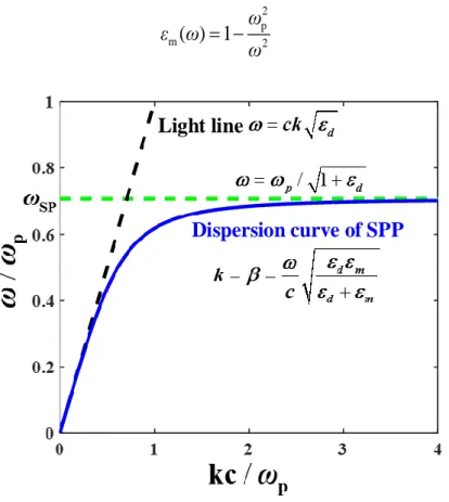
interband transitions, the permittivity of a lossless metal is 2 p m( ) 1 2 ω ε ω ω (1.4) Light line Dispersion curve of SPP
Fig. 1.7 Dispersion relation of surface plasmon polariton at a metal-dielectric interface without considering the loss of metal.
Fig. 1.7 shows the obtained dispersion relation of the SPP mode at a metal-dielectric interface without considering the loss of metal. The black dashed line is the light line in the dielectric. We can see that the propagation constant of the SPP wave is larger than the one of the light line. This leads to two consequences. Firstly, special phase-matching techniques based on grating or prism coupling are required for the excitation of SPP from a free space or fiber optical beam. Secondly and importantly, it results into better confinement of light than in dielectrics. To understand this point, let us have a look to the following equations
2 2 2 d 0 d d d 2 2 2 m 0 m m m , 1/ , 1/ k β k ε δ k k β k ε δ k (1.5)
two media. δd,m are the evanescent decay lengths of the fields perpendicular to the interface, which quantify the confinement of the wave. As εm is negative and has a large absolute value, the penetration depth of light into the metal is always small. As shown in Fig. 1.7, for small ω values, β is very close to k0 ε and the SPP dispersion curve d follows the light line very closely. In this case kd is very small and inversely δd is large, thus the SPP wave extends deep into the dielectric. As ω increases, the difference between β and k0 ε also increases. Correspondingly, kd d becomes larger and δd becomes smaller, which means better confinement of light in the dielectric side. Especially, when ω approaches the surface plasmon resonance frequency (ωSP), β approaches infinity. ωSP is expressed by
p SP d 1 ω ω ε (1.6)
Near the surface plasmon resonance frequency, the wave greatly slows down and the extent of the field on either side of the interface becomes vanishingly small. While another important characteristic parameter of the SPP mode: the propagation distance Lp, which is defined as the distance over which the power drops to 1/e of its initial magnitude and given by:
p 1 2 Im[ ] L β (1.7) becomes shorter.
To provide here a quantitative idea of the involved orders of magnitude regarding especially the evanescent decay length and propagation distance, we plot them as a function of wavelength in Fig. 1.8 for a silver-air interface. As the wavelength decreases, the SPP mode appears to have a better confinement on the dielectric side (let us notice that d is expressed in µm), while the fraction of the field concentrated in the metal
decreases to shorter values due to ohmic absorption in the metal. We can see here the propagation distance of SPP is on the order of millimeters, actually it will become shorter for other metals and dielectrics and roughness of interface in practical demonstrations. The losses have long been the biggest challenge of plasmonics and thus need to be managed carefully. Normally, people tend to use hybrid plasmonic structures with dielectrics, in which the loss penalty is less strong. As a matter of fact, after roughly a decade of research and development, researchers in the field have managed to figure out some potential methods to deal with this biggest challenge [50].
0.6 0.8 1 1.2 1.4 1.6 1.8 2 0 1 2 3 4 5 0.6 0.8 1 1.2 1.4 1.6 1.8 2 0 0.5 1 1.5 2 2.5 0.6 0.8 1 1.2 1.4 1.6 1.8 2 21.5 22 22.5 23 23.5 ( )
Wavelength μm Wavelength μm ( ) Wavelength μm ( )
d ( μ m) δ (m nm ) δ (p m m ) L (a) (b) (c)
Fig. 1.8 Penetration depth into the (a) dielectric and (b) metal and (c) propagation distance of the SPP wave at the silver-air interface as a function of the wavelength.
Recently, M. L. Brongersma comprehensively summarized five strengths of plasmonics in a review paper as follows [51]: (1) extreme light concentration and light manipulation below the free space diffraction limit; (2) straightforward tunability of the optically-resonant response of metallic nanostructures by engineering their size, shape or dielectric environment; (3) simple building blocks offer a tremendous design flexibility to create a large number of optical functions; (4) efficient light-to-heat conversion with high spatial and temporal control; (5) multifunctionality of nanometallic elements in a single physical space.
These attractive strengths make plasmonics finding applications in many areas of science and technology, including plasmon-assisted catalysis, nanoscale thermal engineering for nanostructure synthesis and phase transformations, heat-assisted magnetic recording and treatment of cancer, optical trapping and sensing, optical
imaging and lithography, engineering emission from quantum emitters, thermal radiation engineering, ultrafast and nonlinear plasmonics, plasmonics for solar energy harvesting, and active chipscale plasmonic devices including most notably nanoscale sources, modulators and detectors [51].
1.3 Nonlinear silicon plasmonics
First of all, let us give a brief introduction to nonlinear optics. In nonlinear optics, the total polarization P t( ) induced by electric dipoles is not linear in the electric field E t( ), but satisfies the more general relation [52]:
(1) (2) (3)
0
( ) [ ( ) : ( ) ( ) ( ) ( ) ( ) ]
P t E t E t E t E t E t E t (1.8) where χ(1) is known as the linear susceptibility. In the case of linear optics, the induced polarization depends linearly on the electric field strength. χ(2) and χ(3) are known as the second- and third-order nonlinear optical susceptibilities, respectively. In general, χ(i) is a tensor of rank i + 1. In the forms shown, we have also assumed an instantaneous response of the polarization to the electric field strength. The second-order optical nonlinearity vanishes in centrosymmetric crystals, while the third-order nonlinear optical interactions can occur for both centrosymmetric and noncentrosymmetric media. Common second-order nonlinear effects include second harmonic generation, sum frequency generation, difference frequency generation, Pockels effect (also known as electro-optic effect) and optical rectification effect. Frequently-used third-order nonlinear effects include third harmonic generation, four-wave mixing, self-phase modulation, and cross-phase modulation. These diverse nonlinear effects provide much more degrees of freedom to control the optical field, which make nonlinear optics playing a great impact in today’s daily life, such as in the fields of lasers, material interactions and information technology [53].
photonics and considerably studied for electro-optic modulation, all-optical signal processing, generation of ultra-short pulses, and ultrafast switching [20, 54]. Realizing efficient optical nonlinear effects at nanoscales and within short distances plays a key role in improving the density and reducing the power consumption. Plasmonics opens up an opportunity to simultaneously increase device nonlinear efficiencies, reduce device power consumptions and footprints, speed up the device response time and improve the device flexibility. In principle, the role of plasmonics in nonlinear optics is threefold. Firstly, the strong optical field and related enhanced nonlinearity in plasmonic nanostructures allows nonlinear effects to be utilized with reduced optical power. Secondly, they scale down the sizes of nonlinear components, which is important for the development of integrated photonic devices and, ultimately, of the fully functional nanophotonic circuitry. Thirdly, the response time of plasmonic excitations is ultrafast, allowing optical signals to be manipulated on femtosecond timescales. The detailed principle and applications for the field of nonlinear plasmonics can be found in a good review paper of Ref. [20]. Here we just want to highlight the mentioned research status and elicit the next development expectations of the field.
With the continuous development of modern nanofabrication technique, precisely experimental implementations of nonlinear plasmonic devices are possible and demonstrated in plenty of reports. However, with few exceptions the majority of experiments on nonlinear plasmonics have involved free-space beams at least for signal or control light. For certain applications, it is necessary to design systems where all
beams are maintained within the integrated plasmonic circuitry [20]. In the same time,
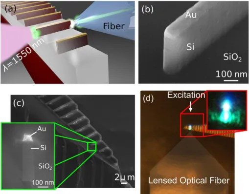
the compatibility with silicon photonics is also strongly expected. To our best knowledge, few work especially experimental demonstrations have been reported to address these two expectations together. The aforementioned POH modulators belong to one of them. As another example, S. Sederberg et al. recently demonstrated for the first time an efficient third harmonic generation in a silicon-based nanoplasmonic waveguide. As show in Fig. 1.9, the proposed waveguide consisting of a silicon core
and a gold cap is simple to fabricate, compatible with modern electronics and photonics technologies, and occupies an ultracompact footprint of 0.40 μm2. Femtosecond laser pulses at λ = 1550 nm with input powers in the range of 85 μW – 1.52 mW are used to generate strong THG. The conversion efficiencies is up to 2.3 × 10⁻⁵ with waveguide length of 5 μm, which is the highest reported to date in any silicon-based device or nanoplasmonic structure [55].
Fig. 1.9 Efficient third harmonic generation in a silicon-based nanoplasmonic waveguide. Figure taken from Ref. [55].
We define the system in which all beams are maintained in the integrated plasmonic circuitry and compatible with silicon photonics as the silicon plasmonic platform. Nonlinear silicon plasmonics is still a young research field, but its basic concepts and great potential have been proposed in a wide variety of ways already. At present, precise experimental fabrication and measurement of the nanoscale silicon plasmonic waveguides is still a big challenge and concepts for more sophisticated waveguide designs and more complex nonlinear effects need to be investigated. Nevertheless, we envisage the field to become increasingly important in the
development of the future integrated nanophotonics, just as traditional nonlinear silicon photonics was in shaping the landscape of modern integrated photonics.
Taking both expectations in mind, in this dissertation we have designed and investigated different kinds of nonlinear silicon plasmonic waveguides and exploited the effective nonlinear effects induced in the nanoscale plasmonic waveguide for optical signal processing.
1.4 Organization
The organization of the dissertation is as follows.
In chapter 2, we firstly give a brief review on the plasmonic waveguides. Especially, we primarily focus on two kinds of waveguides: plasmonic slot waveguides (PSW) and hybrid plasmonic waveguides (HPW). Then, we derive the theoretical model of nonlinear coupled-wave equations which have been used to analyze the nonlinear effects in silicon plasmonic waveguides with losses and for the investigation of the mechanisms proper to enhance optical nonlinear effects.
In chapter 3, we investigate the possibility of enhancing nonlinear effects based on the PSW and the related applications in optical signal processing. Specifically, three kinds of nonlinear effects are studied, including the enhanced second harmonic generation (SHG), a new high-speed electrooptic modulation mechanism based on the electrically controlled SHG and high-speed optical detection based on the optical rectification effect.
In chapter 4, we focus on the HPW-based nonlinear enhancement. Efficient SHG and optical parameter amplification (OPA) are analyzed. The SHG is then further enhanced by using HPW-based ring resonators. The OPA can be applied to regenerate the phase shift keying optical signals.
demonstrate the optical rectification effect proposed in chapter 3. The chapter includes the design, fabrication and measurement of the structures. By spin-coating an EO polymer onto PSW, the nonlinear property of the coated PSW is investigated.
Chapter 2
Theoretical analysis of nonlinear processes in silicon
plasmonic waveguides
We aim in this dissertation at investigating the potentials of the combination of silicon photonics and plasmonics for the design of photonic integrated circuits and functions. We will focus on a particular aspect of this research field, called silicon plasmonics: the enhancement of nonlinear effects by using plasmonic structures.
In this chapter, we firstly give a brief review of the main plasmonic waveguides proposed in previous works and then focus on two kinds of plasmonic waveguides that can easily be integrated within the silicon photonics platform. In the second part, we derive a set of nonlinear coupled-wave equations (NCEs) which can be exploited to analyze the nonlinear effects induced in the lossy plasmonic waveguides. Note that the NCEs have been widely addressed before in fibers [56] and silicon waveguides [29, 57], in which the losses are negligible. While, in plasmonic waveguides the loss cannot be neglected and thus in the derivation of NCE the normalization condition needs to be considered in term of the unconjugated reciprocity theorem [58, 59]. In Ref. [59], the researchers have done similar derivations to model the optics-to-THz conversion in metallic slot waveguides. Here in this manuscript, we obtain a general form of NCE both in the frequency and time domains that can be used to model any kind of nonlinear optical effects induced in a lossy waveguide. Lastly, four general guidelines for the design of integrated waveguides providing strong nonlinear effects are put forward based on the proposed NCEs.
2.1 Silicon plasmonic waveguides
plasmonic waveguides have attracted a growing interest in the last decade. Many kinds of nanoscale plasmonic waveguides have been proposed theoretically and demonstrated experimentally, such as metal nanowire waveguides [60-62], metal nanoparticle chain array waveguides [63-66], channel plasmon waveguides being constructed by V-grooves in metals [67], plasmonic slot waveguides (or so called metal-dielectric-metal waveguides in two-dimensional case) consisting of a slot sandwitched between two metallic regions [68-72], long range plasmonic waveguides (or so called dielectric-metal-dielectric waveguides in two-dimensional case) comprising a finite-width metal stripe surrounded by dielectric media [73-75], hybrid plasmonic waveguides being made up of a high refractive index (RI) dielectric material separated from the metal part by a subwavelength low RI dielectric gap [76-79], and dielectric loaded plasmonic waveguides made of a dielectric ridge placed on a metal surface [80-82].
All these plasmonic waveguides are able to support tight confinement of optical fields in two directions to the nanoscale that dielectric waveguides unable to do. However, the losses come along with the tight confinement. In plasmonic waveguides, generally there exists a trade-off between confinement and loss. Better confinement is always accompanied by larger losses. This point can be fundamentally understood from Fig. 1.8 for the SPP mode at a metal-dielectric interface: for smaller wavelengths it supports better confinement in the dielectric (Fig. 1.8(a)), while the fraction of the field concentrated in the metal increases (Fig. 1.8(b)). The propagation distance thus decreases to shorter values due to larger ohmic absorption in the metal (Fig. 1.8(c)).
In the early stages, the priority was to realize the best confinement of the optical field, while the loss issue was not considered so much. In the initially proposed plasmonic waveguide structures, such as metal nanowire waveguides, nanoparticle array waveguides and channel plasmon waveguides shown in Fig. 2.1, even though ultra-highly localization of the optical field into nanometer scales was achieved, the related structures had large losses, meaning that only short propagation distances (usually ~μm) were possible. Besides, the fabrication and precise control of these
waveguide were complex due to their nonrectangular shapes. Additionally, as the related devices were hardly compatible with the silicon photonics platform, we have not considered them in the present manuscript for the design of plasmonic-enhanced nonlinear optical functions on silicon.
(a) (b) (c)
Fig. 2.1 Initially proposed plasmonic waveguides: (a) metal nanowire waveguides [61], (b) metal nanoparticle chain waveguides [65, 66] and (c) channel plasmon waveguides [67]. They can confine the optical field into nanometer scales, while the losses are usually large.
(a) (b)
20 × 20 µm2
Fig. 2.2 (a) Long range plasmonic waveguide made of a gold stripe with width of 4 μm and thickness of 25 nm. (b) mode intensity contours plotted over a 20 × 20 μm2
cross-sectional domain. Figure taken from [74].
In an opposite direction, the long range plasmonic waveguides enable long propagation distances, but their confinement properties show in fact no advantage if
compared with conventional dielectric waveguides. Fig. 2.2 shows the schematic and mode profile of a typical long range plasmonic waveguide. By considering an gold stripe with width of 4 μm and thickness of 25 nm, the experimental measured loss is 1.07 dB/mm at λ = 1550 nm, while the mode extends several micrometers away from the metal stripe [74]. Thus, this kind of waveguides has been disregarded in the investigations performed in this manuscript.
Beyond these two extreme cases, the loss/field-confinement compromise of
plasmonic waveguides can fortunately be adjusted by a proper choice of the waveguide material and geometry cross-section. Plasmonic slot waveguides, hybrid plasmonic waveguides and dielectric loaded plasmonic waveguides, as shown in Fig. 2.3, have been proposed in this purpose. These waveguides can also be experimentally realized with the standard CMOS technology, belong to the previously mentioned silicon plasmonic waveguides.
(a) (b) (c)
Fig. 2.3 Silicon plasmonic waveguides have better compromise between confinement and loss. (a) plasmonic slot waveguides [72], (b) hybrid plasmonic waveguides [79], and (c) dielectric loaded plasmonic waveguides [81].
The works reported in this manuscript have been mostly based on plasmonic slot waveguides and hybrid plasmonic waveguides. So in the next, we will give a more detailed introduction to these two waveguide families. We will see that due to the
difference of the mode confinement mechanism and loss level, they are suitable for different nonlinear applications.
2.1.1 Plasmonic slot waveguides
In view of the strong localization of optical field on a single metal/dielectric interface on the dielectric side due to the large discontinuity difference of the material permittivities, it is intuitive to closely combine two interfaces to form the so-called metal-dielectric-metal waveguide. In a realistic planar scheme, one gets the so-called plasmonic slot waveguide (PSW).
SiO2 Silver Silver w h Air Substrate Metal Metal w = 100 nm h = 150 nm
Fig. 2.4 Typical configuration and calculated field distribution for the major component Ex
of the fundamental mode of a plasmonic slot waveguide with w = 100 nm and h = 150 nm. One sees that the field is highly localized and greatly enhanced in the nanoscale slot.
Fig. 2.4 shows the typical configuration and mode profile of a PSW. The SPPs on two surfaces that exist in the PSW couple to each other and result in a strong localization of the field in the slot area. The slot width can be chosen down to a few tens of nanometers. Actually, this waveguide geometry is very similar to the silicon slot waveguides, as proposed by Almeida and co-workers [83]. Merely the amplitude of the real part of the metal permittivity is even larger than the one of silicon, which makes PSW have an even larger enhancement of optical fields in the slot region than their dielectric counterparts. To have a more quantitative vision, we plot in Fig. 2.5 the mode effective index neff, propagation length Lp and mode effective area Aeff of the fundamental mode in PSW as a function of slot width w for different slot height h. Aeff,
whose definition can be found in Section 2.2.2 by Eq. (2.19), is a very key parameter in nonlinear enhancement. Note here that these parameters and all other waveguide mode calculations performed by us have been calculated by a finite element method based commercial software (COMSOL Multiphysics) [84].
(a) (b)
(c) (d)
50 nm 10 nm
Fig. 2.5 (a) Mode effective index neff, (b) propagation length Lp and (c) mode effective area Aeff of the fundamental mode in PSW as a function of slot width for different slot height.
(d) The electric field distribution when w = 10 nm and h = 50 nm. The optical wavelength is fixed at λ = 1550 nm.
The metal, substrate and cladding materials are chosen to be silver, SiO2 and air, respectively. As the slot width decreases, the impact of the height on the mode property becomes weaker. Meanwhile, neff increases, while the loss becomes larger. Especially, as shown in Fig. 2.5(d), PSW is capable of guiding a highly confined mode at λ = 1550 nm into a slot as small as 10 nm × 50 nm. The corresponding mode effective area is as small as 2.04 × 10⁻¹⁵ m2, which is down to λ2/1200. However, Lp decreases to 9.35 μm. Therefore, there usually exists an optimized dimension in PSW-based optoelectronic devices for realizing best device performances. This will be seen in Chapter 3.