HAL Id: tel-01429670
https://tel.archives-ouvertes.fr/tel-01429670
Submitted on 9 Jan 2017
HAL is a multi-disciplinary open access archive for the deposit and dissemination of sci-entific research documents, whether they are pub-lished or not. The documents may come from teaching and research institutions in France or abroad, or from public or private research centers.
L’archive ouverte pluridisciplinaire HAL, est destinée au dépôt et à la diffusion de documents scientifiques de niveau recherche, publiés ou non, émanant des établissements d’enseignement et de recherche français ou étrangers, des laboratoires publics ou privés.
Charge transport in disordered organic semiconducting
dendrimers studied by space-charge-limited transient
currents
Marek Zdzislaw Szymanski
To cite this version:
Marek Zdzislaw Szymanski. Charge transport in disordered organic semiconducting dendrimers stud-ied by space-charge-limited transient currents. Condensed Matter [cond-mat]. Université de Grenoble, 2012. English. �NNT : 2012GRENY065�. �tel-01429670�
THÈSE
Pour obtenir le grade de
DOCTEUR DE L’UNIVERSITÉ DE GRENOBLE
Spécialité : Physique de la matière condensée et du rayonnement
Arrêté ministériel : 7 août 2006
Présentée par
Marek Zdzisław Szyma ´nski
Thèse dirigée par David Djurado
préparée au sein du Laboratoire d’Electronique Moléculaire Organique & Hybride, INAC/SPrAM (UMR-5819), CEA Grenoble
et de l’Ecole Doctorale de Physique de Grenoble
Charge transport in disordered
or-ganic semiconducting dendrimers
studied by space-charge-limited
transient currents
Thèse soutenue publiquement le 15 novembre 2012, devant le jury composé de :
M. Alasdair Campbell
Senior Lecturer of Imperial College London, Rapporteur M. Gilles Horowitz
Professor of Ecole Polytechnique, Rapporteur M. Beat Ruhstaller
Professor of Zurich University of Applied Science, Examinateur M. Jean-Pierre Travers
Directeur de recherche CNRS, CEA Grenoble, Examinateur M. David Djurado
Summary: The thesis concerns space-charge-limited transient current measurements in thin (≤ 500nm) organic films. Such films find important applications in organic electronics, where they are referred to as organic semiconduc-tor layers. Electrical transport in such films depends on bulk charge carrier transport and trapping, as well efficiency of charge carrier injection from electrodes. These, are all in turn depend on disorder inherent to organic materials. The transient measurement approach is very attractive, as it can, in principle, deliver information on all these aspects in one single measurement. In the thesis, three main contributions are presented: 1) A transimpedance amplifier based setup for space-charge-limited current transient measurement is validated. This type of setup is superior to the widely used bridge circuit, notably because of better current sensitivity, bandwidth, no need for bridge symmetry and no need for per sample adjustment. It is demonstrated that initial displacement current spike, which saturates the amplifier at the beginning of measurement, does not introduce error in the measurement of mobility. 2) A dendrimer molecule has been investigated. Experimental current responses are shown to be in agreement with the drift-diffusion model. However, obtaining agreement requires well defined initial conditions in experiment as well as in simulation, and also complete theoretical model of the sample. In the case of dendrimer, this model had to take into account both contact barrier and trapping effects. Furthermore, better agreement was obtained when taking disorder effects into account. 3) The impossibility of obtaining any agreement without complete physical model of the sample indicates that trapping, contact barrier and mobility parameters could be fitted without ambiguity. Therefore, complete elec-trical characterization consistent with simulation can be obtained using the transient technique. The results obtained further increase well known usefulness of transient space-charge-limited current characterization of thin organic films.
Résumé : La thèse porte sur les mesures de courants transitoires limités par la charge d’espace dans des films minces organiques (épaisseur < 500 nm). Ce type de films est souvent utilisé dans des applications dans le domaine de l’électronique organique comme couches actives semi-conductrices. Le transport électrique dans ces films dépend en premier lieu du transport des porteurs de charge dans le milieu massif et de leur piégeage, mais aussi de l’efficacité de l’injection des porteurs de charges à partir des électrodes métalliques. L’ensemble est de plus conditionné par le taux de désordre inhérent aux matériaux organiques. L’approche qui consiste à utiliser la mesure de courants transitoires est extrêmement attractive car elle permet en principe de fournir une information sur tous ces aspects à l’issue d’un seul type de mesure. Dans ce cadre, trois contributions principales peuvent être dégagées de la thèse : 1) Tout d’abord, nous avons validé un montage expérimental qui utilise un amplificateur à transfert d’impédance pour la mesure des courants transitoires limités par la charge d’espace. Ce type de montage s’avère supérieur au circuit de pont électrique le plus largement utilisé jusqu’à maintenant car il présente une meilleure sensibilité en courant, une meilleure bande passante, et ne nécessite aucun réglage ni de la symétrie du pont ni de l’ajustement de la taille de l’échantillon. On a pu démontrer que le pic de courant de déplacement initial, qui sature l’amplificateur au tout début de la mesure n’introduit pas d’erreur dans la mesure de la mobilité. 2) Ensuite concernant l’étude plus spécifique du transport dans un dendrimère à base de tri-arylamine, les réponse en courant obtenues expérimentalement se sont avérées en bon accord avec le modèle de déplacement-diffusion. Cependant, la troisième leçon que nous avons apprise est que l’obtention d’un tel accord a nécessité que soient très bien définies les conditions initiales tant de l’expérience que de la simulation et qu’un modèle théorique le plus complet possible de l’échantillon soit considéré. Pour le dendrimère ce modèle a dû prendre en compte l’effet de la barrière au contact et les effets de piégeage. Un accord encore meilleur a été obtenu en intégrant de surcroit les effets de désordre. 3) La complète impossibilité d’obtenir un bon accord sans un modèle physique complet de l’échantillon indique que les paramètres liés au piégeage, à la barrière au contact et à la mobilité peuvent véritablement être ajustés sans aucune ambigüité. Ainsi, une caractérisation électrique complète en cohérence avec la simulation a pu être obtenue à l’issue d’un seul type de mesures. Les résultats obtenus, alliant à la fois amélioration technique et support numérique, témoignent de la grande utilité de cette technique de mesure de courant transitoire limité par la charge d’espace pour caractériser en détails le transport dans les films minces organiques.
Charge transport in disordered organic
semiconducting dendrimers studied by
space-charge-limited transient currents
This thesis is dedicated to my parents : my mother Irena and the memory of my father, Aleksander Bożymir.
Contents
Résumé de la thèse iii
Acknowledgments 1
Introduction 3
Chapter 1. Charge carrier transport in organic layers 5
1.1. Transport model 5 1.2. Space-charge-limited current 7 1.3. Importance of diffusion 9 1.4. Metal-organic interface 9 1.5. Effects of traps 11 1.6. Injection-limited current 15 1.7. Transient response 17 1.8. Conclusions 21
Chapter 2. Gaussian disorder model and its application to space-charge-limited case 25 2.1. Gaussian disorder model 25 2.2. Effect of tail states filling: Master equation approach 29 2.3. Generalized Einstein relation 32 2.4. Metal-organic interface(2) 33
2.5. Conclusions 37
Chapter 3. Drift-diffusion simulation 38
3.1. Overview 39
3.2. Scharfetter-Gummel discretization 41 3.3. Solving and convergence 46
3.4. Timestepping 48
3.5. Adaptation for organic materials 49
3.6. Implementation 50
3.7. Conclusions 52
Chapter 4. Transient current measurements using transimpedance amplifier 53
4.1. Bridge circuit 56
CONTENTS ii
4.2. Transimpedance circuit 58 4.3. Bandwidth and stability 60
4.4. Initial saturation 62
4.5. Practical realization 63
4.6. Characterization 65
4.7. Verification 67
4.8. Conclusions 68
Chapter 5. Results obtained on one triarylamine based dendrimer 70
5.1. Sample preparation 70
5.2. Single transient measurements 73 5.3. Repeated transient measurements 77
5.4. Aging changes 78
5.5. Conclusions 80
Chapter 6. Comparison experiment simulation 82 6.1. Initial conditions problem 84
6.2. Fitting method 87
6.3. Results 91
6.4. Conclusions 98
Conclusions and outlook 100
List of contributions 103
Bibliography 105
Appendix A. Electrochemical and chemical characterizations of triarylamine based
dendrimer DT1Bu6 112
A.1. Chemical formula and synthesis 112 A.2. Optical spectroscopy 113 A.3. Electrochemical measurements 114 Appendix B. Simulation program (dd2) 117
B.1. Running dd2 117
B.2. Parameters 118
B.3. Models 121
B.4. Functions 122
Résumé de la thèse
Dans le domaine dénommé généralement l’électronique organique, on peut distinguer un courant qui se propose en particulier de développer des nouveaux dispositifs optoélectro-niques, en particulier des écrans et des cellules photovoltaïques. Une des motivations serait un cout de fabrication par unité d’aire nettement plus bas que pour les dispositifs conven-tionnels. Egalement, ces dispositifs peuvent présenter des caractéristiques attractives pour leur utilisation quotidienne telle que par exemple une bonne flexibilité mécanique.
Dans ce but, une intense activité de recherche est aujourd’hui concentrée autour des maté-riaux organiques électroniques et des dispositifs prototypes. Une grande partie des contribu-tions scientifiques concerne donc la synthèse de ces matériaux, ainsi que leur mise en œuvre. En parallèle, un effort constant est fait pour améliorer l’élaboration de modèles physiques du transport dans les matériaux organiques. Malheureusement, il existe encore trop peu de connexions entre ces deux champs de recherche réclamant des expertises différentes. Les théories physiques sont ainsi vérifiées et développées sur la base d’un nombre plutôt faible de matériaux parmi les plus connus. L’analyse des propriétés observées s’arrête encore trop sou-vent aux concepts physiques de base. Ceci bien sûr s’explique par le degré de complexité des solides organiques et le caractère inévitablement pluridisciplinaire que leur approche réclame. Dans cette thèse, l’effort produit pour contribuer à l’électronique organique ne se situe ni au niveau de l’étude de nouveaux matériaux ni sur celui du développement de la théorie du transport, mais cherche à simplifier l’utilisation d’une des techniques les plus puissantes de mesure du transport et à rendre disponible un plus grand nombre d’options pour l’analyse des données. De cette manière, nous espérons que la technique améliorée sera plus facile à mettre en œuvre et permettra plus aisément de vérifier les modèles physiques existants en donnant accès à des paramètres physiques fondamentaux permettant de mieux comprendre les performances des dispositifs mais qui ne sont pas directement mesurables. En retour, notre démarche peut aider à l’optimisation des matériaux et de leur mise en œuvre.
La technique expérimentale dont il est question est celle de la mesure de courants tran-sitoires limités par la charge d’espace (aussi connue sous le nom de mesure transitoire de l’injection en obscurité). C’est une des nombreuses techniques utilisées pour la caractérisa-tion électrique des matériaux organiques mais est sans doute une des moins populaires[1]. Ses propriétés uniques apparaissent rapidement quand on la compare à d’autres techniques bien connues. Jusqu’à présent, elle a surtout été utilisée pour la mesure de la mobilité des
RÉSUMÉ DE LA THÈSE iv
porteurs et la caractérisation de l’efficacité des contacts. En effet, comme cette technique permet d’obtenir une bonne estimation de la mobilité qui soit relativement peu affectée par l’efficacité des contacts, elle commence maintenant à être plus largement appliquée aux films organiques minces. A ce titre elle pourrait devenir une technique de caractérisation stan-dard de ces matériaux. Cependant, les mesures de courants transitoires ne sont pas triviales car elles comportent des difficultés expérimentales importantes. A cause de cela, récemment dans la littérature des questions sont apparues quant à la pertinence et la précision réelle de cette méthode ainsi que sur le degré d’accord des résultats qu’elle fournit avec les prédictions théoriques [2].
Il faut d’abord considérer, qu’en dépit du caractère crucial que revêt la détermination de la mobilité des porteurs de charges, les performances des contacts sont tout aussi cruciales dans la détermination de celles des dispositifs. Jusqu’à présent, il n’existe pas à notre connais-sance de technique de mesure admise définitivement ainsi qu’une approche théorique pour traiter de cette question. Puisque l’interface est enterrée en dessous de l’électrode, elle n’est pas directement accessible pour l’étude. Des performances parfois très différentes de celles prédites à partir de mesures spectroscopiques comme l’UPS peuvent être ainsi obtenues. La voltamétrie cyclique, technique d’électrochimie, souvent utilisée pour prédire le caractère oh-mique des contacts est en fait non justifiée pour cette application et utilisée à mauvais escient [3]. Donc, au delà de la mesure de la mobilité, la possibilité d’une caractérisation quantitative et prédictive de ces interfaces revêt une grand importance.
La thèse s’ouvre sur deux chapitres en forme de revues.
Le chapitre 1 reprend l’approche de base du transport de porteurs de charge dans les maté-riaux organiques semi-conducteurs. Ces matématé-riaux sont de manière intrinsèques des isolants, du fait qu’ils présentent une concentration négligeable de porteurs libres. Il est cependant possible de générer des porteurs libres par injection à partir d’électrodes, par dopage ou encore par excitation optique[4]. Ce travail s’intéresse exclusivement au premier cas et par conséquent ce chapitre traite exclusivement de l’injection de courant dans les isolants. Il in-troduit d’abord le modèle de déplacement-diffusion et le calcul de la loi de Mott-Gurney qui peut en être déduit. Les prédictions que l’on peut tirer de cette loi analytique négligeant la diffusion sont ensuite comparées avec des simulations qui prennent en compte la diffusion. Cela permet de cerner les limitations de l’expression analytique de la loi quand on considère précisément les matériaux organiques semi-conducteurs. Ensuite, toujours dans ce chapitre, la théorie qui néglige le désordre est présentée mais les effets du piégeage et de la barrière au contact sont considérés et leur influence sur les caractéristiques courant tension est discutée. La partie la plus grande de ce chapitre est consacrée à l’examen de la réponse transitoire en courant de films organiques fins. Un traitement théorique simple de ces réponses transitoires
RÉSUMÉ DE LA THÈSE v
est proposé. Des résultats de simulation des réponses transitoires affectées par l’effet de pié-geage et de la barrière au contact sont aussi présentés. On en conclut que caractériser les matériaux organiques en utilisant des techniques transitoires permet d’éviter de nombreux problèmes par ailleurs associés aux mesures courant-tension stationnaires.
Le chapitre 2 est dédié à une revue plus détaillée de l’influence des mécanismes microsco-piques du transport sur ses propriétés mesurées macroscopiquement. En général on s’accorde pour dire que le transport procède par sauts entre états localisés. Parmi les multiples théo-ries, celle du modèle du désordre Gaussien de Baessler et ses extensions s’est montré capable d’expliquer et d’unifier les observations expérimentales à la fois dans les matériaux molécu-laires et les polymères. Dans ce chapitre, ce modèle est donc d’abord introduit. Il est connu que ce modèle prédit l’influence de la température et du champ électrique sur la mobilité des porteurs dans les matériaux organiques dans l’approximation d’un porteur de charge unique. Or, cette approximation n’est pas bonne dans les conditions de limite par la charge d’espace. Cela nous amène à discuter des effets de remplissage des états des bords de la densité d’états Gaussienne. A ce point, nous introduisons la relation entre la densité de porteurs de charge et la mobilité en adoptant une approche qui utilise les équations maitresses. Un autre point im-portant que nous soulevons, est que dans le cas d’une densité d’états Gaussienne, une version généralisée de la relation d’Einstein doit être utilisée et nous discutons aussi ce point. Enfin, on explique comment la notion de désordre permet un traitement plus détaillé de l’injection des porteurs de charge aux électrodes en posant les conditions de l’équilibre thermique local. Le modèle de déplacement-diffusion introduit au chapitre 1, même dans sa forme la plus simple ne peut pas être résolu analytiquement. Les simplifications qui pourraient permettre de le faire peuvent déboucher sur des erreurs significatives. Ainsi, nous avons été amenés pour cette thèse à développer un outil de simulation numérique. Cet outil est capable de ré-soudre des problèmes tant stationnaires que transitoires, prenant en compte tous les modèles de contact, de piégeage et de mobilité développés dans les chapitres précédents 1 et 2. Les approches possibles pour la simulation du transport électrique dans les solides organiques, ainsi que la conception du simulateur sont décrits dans le chapitre 3. Le simulateur permet de résoudre de manière couplée les équations du transport et l’équation de Poisson, en utilisant le procédé de discrétisation de Scharfetter-Gummel. Cette méthode [5] fait appel à une inter-polation exponentielle de la concentration des porteurs de charges entre les nœuds du la grille de simulation. C’est un moyen d’assurer le signe positif de la concentration des porteurs et d’assurer un profil abrupt du gradient de concentration dans les dispositifs sans nécessiter le recours à une grande densité d’échantillonnage pour la grille de simulation. L’ensemble résul-tant d’équations non linéaires est alors résolu en utilisant la méthode de Raphson-Newton à l’aide d’un Jacobien analytique. L’échantillonnage temporel est assuré par la méthode impli-cite d’Euler. Cet échantillonnage peut être automatiquement réglé, en utilisant une approche
RÉSUMÉ DE LA THÈSE vi
“Proportionnel Intégrale Dérivé”. C’est très pratique pour les simulations transitoires avec les effets de pièges, car l’impulsion initiale de courant est suivie ensuite par une longue décrois-sance du courant qui ne varie que très peu en amplitude. Le simulateur a été écrit en langage Python en utilisant PySparse pour la résolution des matrices creuses.
La partie totalement originale de la thèse est contenue dans les chapitres4, 5 et 6.
Le chapitre 4présente en détails les conditions expérimentales utilisées pour les mesures de courants transitoires. De grandes difficultés expérimentales proviennent directement de la capacité géométrique de l’échantillon. Afin de minimiser ces effets, le circuit en pont est fréquemment utilisé. Ceci permet effectivement de soustraire la contribution capacitive du courant de déplacement du signal total mesuré, ce qui rend plus facile l’identification du pic en courant limité par la charge d’espace. Nous avons pour notre part développé une approche plus simple faisant appel à l’utilisation d’un amplificateur à transimpédance. L’amplificateur à transimpédance convertit directement en tension le signal mesuré en courant. Ceci per-met, et c’est de la plus haute importance, d’éviter toute introduction de résistance en série dans le circuit. Cependant, cette méthode est aussi affectée par la contribution de courant de déplacement. Cette contribution capacitive va provoquer une condition de surcharge de l’amplificateur, qui potentiellement peut conduire à un temps mort expérimental et peut être à une distorsion du signal de sortie. Dans ce chapitre on montre en particulier en s’ap-puyant sur une mesure des caractéristiques d’un semi-conducteur organique bien connu dans le domaine (le PCBM dérivé du fullerène C60) que ces effets n’empêchent pas la mesure. La position temporel du pic est indépendante du type d’amplificateur à transimpédance utilisé à performances équivalentes par ailleurs. Ainsi, l’approche que nous proposons s’est avérée fiable pour permettre l’extraction de la valeur de la mobilité dans le matériau. On peut également souligner que cette approche basée sur l’utilisation d’un amplificateur à transim-pédance, comparée à celle utilisant un pont, supprime le besoin d’ajuster spécifiquement la taille de l’échantillon tout en offrant une meilleure sensibilité en courant, et même en per-mettant des mesures plus rapides. Ceci est d’autant plus intéressant qu’il a été montré que cet ajustement nécessaire de l’échantillon était une des sources principales d’imprécision de la méthode utilisant un pont [2].
Une fois cette approche expérimentale validée, nous l’avons utilisée pour caractériser le transport des trous dans un dendrimère à base de triarylamines nouvellement synthétisé par nos collaborateurs en Pologne et les résultats sont reportés dans le chapitre 5. Nous avons trouvé une valeur de 8 × 10⁻⁶cm2/(V s) pour la mobilité dans ce matériau, ce qui est très
proche des valeurs obtenues dans des composés similaires [6]. A cette occasion, nous avons trouvé que l’or forme des contacts quasi-ohmiques avec le dendrimère, avec une efficacité η ∼ 0.4. Cette observation a été confortée dans la suite du travail quand nous avons comparé des échantillons frais et vieillis. Dans ce dernier cas, l’efficacité du contact s’avère meilleure.
RÉSUMÉ DE LA THÈSE vii
Ce résultat à l’apparence surprenante a déjà été observée dans des travaux antérieurs [7, 8]. Dans le cas du dendrimère, les résultats obtenus nous incitent à attribuer ce comportement à la formation de pièges qui modifie les conditions d’injection. D’autres effets du vieillissement peuvent inclure de manière similaire l’apparition d’impuretés ioniques à l’interface, donnant ensuite naissance à un long déclin du courant (>0.1s). Ces résultats prouvent à l’envi, que l’examen de ces transitoires de courant limité par la charge d’espace ne rend pas seulement possible une caractérisation électrique complète d’un nouveau matériau, mais permet aussi de comprendre son évolution dans le temps.
En plus de cela, nous avons essayé d’observer les effets du piégeage des charges en répétant les mesures des transitoires de courant. Les résultats que nous avons obtenus sont en accord qualitatif avec des simulations, confortant ainsi les suppositions faites pour expliquer les résultats. On a trouvé que les réponses étaient bien reproductibles, si les mesures consécutives sont séparées dans le temps par un temps d’attente suffisamment long (dans notre cas c’était ∼ 0.3s). Si cette condition est satisfaite, même des réponses à des trains d’impulsions longs et compliqués sont très reproductibles. Ainsi, on peut sans crainte procéder à un moyennage afin d’améliorer le rapport signal sur bruit même dans des expériences transitoires de type pompe-sonde, à condition que l’état initial de la mesure soit très bien défini.
La comparaison détaillée entre expérience et simulation des résultats obtenus avec le den-drimère est ensuite présentée dans le chapitre 6.Plusieurs résultats importants sont exposés. Tout d’abord on a démontré que l’état de l’art des modèles du transport dans les matériaux organiques peut reproduire les réponses expérimentales en courant limité par la charge d’es-pace. Un accord bien meilleur que ceux précédemment publiés [2] a été obtenu. On a montré que pour parvenir à un bon accord entre expérience et simulation, il est nécessaire de prendre en compte tous les effets pertinents. Dans notre cas, il s’est agi du transport dans la masse du matériau, le piégeage et la barrière au contact. Tout autre modèle faisant l’impasse sur un de ces effets était en désaccord clair avec l’expérience. Ainsi, tous les paramètres liés à la mobilité, les propriétés des contacts et le piégeage ont pu être extraits de l’analyse. No-tons qu’en dépit d’un accord plutôt satisfaisant, les résultats des ajustements n’étaient pas parfaits en particulier en ce qui concerne le déclin aux temps longs.
Les conclusions ainsi que l’ébauche de directions futures pour ce travail sont donnés ensuite. En résumé, nous retiendrons que nous avons montré que les mesures de courants transitoires limités par la charge d’espace peuvent être techniquement simplifiées et rendues plus faciles d’utilisation en développant un montage expérimental tirant profit des perfor-mances de circuits électroniques désormais disponibles et courants. On a aussi montré que les théories disponibles pour décrire le transport dans des films organiques fins sont capables de reproduire ces expériences et que de nouvelles connaissances peuvent être atteintes grâce à l’analyse numérique des résultats des mesures de courants transitoires.
Acknowledgments
I’m am very grateful to my supervisor, David Djurado, for being the best possible PhD thesis director. David never hesitated to support my ideas and always had time for discussion. And in the mean time, we skied together Sarenne in Alpe d’Huez. It was really a great experience to meet him.
My father, Aleksander Bożymir Szymański (1933-2011), gave me the enthusiasm and the advice necessary to start this work. I would not be able to accomplish it without him. I would equally like to thank my mother, Irena Szymańska, for all her support and help.
This work was made possible by help and advice of many people. I’m not able to thank all of them, and I honestly apologize to those omitted.
I would like to thank Heinz Baessler and Leonard Tykarski for inspiring discussions. I would also like to thank my collaborators and colleagues from CEA Grenoble: Peter Reiss, Jean-Marie Verilhac, Jérôme Faure-Vincent, Benjamin Grevin, Patrice Rannou, Jean-Pierre Travers, Frederic Chandezon, Jean-Francois Jacquot and Adam Proń. Preparation of the patent application would not be possible without help of Sylvie Guillot. Irena Kulszewicz-Bajer synthetised the dendrimer material.
I’m grateful to Beata Łuszczyńska and Magda Kucińska who visited CEA Grenoble. Certainly, the time of their stay was the most interesting and productive of the whole three years.
I would like to thank my friends seen in Grenoble: Tomek Małkiewicz, Mariusz Śliwa, Maria Bacia, Anna Lisowska, Pavol Fedorko, Magda Kucińska, Jarosław Sar, Paweł Gawryś, Jacek Loska and Rasa Sukackaite. I’m specially grateful to Teresa and Jean-Claude Char-bonnel who gave me a new home in St Egreve. I spent much good time with Górski family (Tomek, Beata and Dawid) and Łuszczyński family (Sylwek, Beata, Konrad). I especially thank Tomek Górski who is responsible for some of the most interesting memories of my stay in Grenoble.
I’m grateful to the people who helped me to adapt to living in France. Geneviève Ruissec guided me to say my first words in the French language. Didier from La Charette (St Egreve) introduced me to the French cuisine.
I would also like to thank my professors from the Faculty of Physics at Warsaw University of Technology, who gave me knowledge and confidence necessary to start PhD work. I thank the staff of CEA Grenoble INAC/SPrAM for the reception, and the Commissariat à l’énergie
ACKNOWLEDGMENTS 2
atomique et aux énergies alternatives (CEA) for providing the most of the funding necessary for this work, and in particular, for my PhD scholarship.
Lastly, I would like to thank the members of the jury of this thesis for their numerous remarks and corrections, and for coming to Grenoble for the defence on 15th November 2012.
Introduction
Organic electronics has been proposed to develop novel optoelectronic devices, in partic-ular displays and photovoltaic cells. These are expected to be cheaper to be manufactured, per unit of area, than the conventional devices. Also, they are expected to have desirable features for everyday use, such as mechanical flexibility.
In this aim, there is intense research concentrated on organic electronics materials and devices. Most of contributions is related to material synthesis and preparation techniques. On the other hand, there is a constant improvement in the elaboration of physical models of transport in organic materials. Unfortunately, there is still only a limited connection between these two fields of research. Physical theories are verified, and developed, on rather small amount of well known materials. On the other hand, explanation of observed properties of materials is usually based on the most basic physical concepts. This is well justified by the degree of complexity of organic matter and multidisciplinary character of the work.
In this thesis, effort is made to contribute to organic electronics neither by the investi-gation of new materials, nor by the development of transport theory, but by simplifying the most powerful transport measurement and extending available options of data treatment. By this way, we hope that the improved technique will be easier to be applied and will permit both verification of existing physical models, as well as the estimation of fundamental phys-ical parameters for understanding the performances of devices, but which are not directly measurable. These may in turn help in optimizing the design and processing of the materials. The experimental technique under consideration is space-charge-limited current transient measurement[9, 10] (also known as dark injection transient measurement[11]). It is one of many techniques used for electrical characterization of organic materials, but appears to be one of the least popular (i. e. absent in ref. [1]). Its unique properties are evident in comparison with other well known measurement techniques[12]. Up to now, it has been mainly used as mobility and contact efficiency characterization technique. As this technique permits to obtain a good estimation of mobility relatively unaffected by contact efficiency, it starts to be more widely applied to thin organic films. Because of these, it could be a standard organic semiconductor (insulator) characterization technique. However, transient measurements are not straightforward, and considerable experimental difficulty is associated with it. Also, recently, some questions have been raised about the real accuracy of this method as well as the agreement of obtained results with theoretical predictions[2].
INTRODUCTION 4
It is important to consider, that despite charge carrier mobility is considered as a critical material parameter, contact performance is equally important for device performances[3]. Up to now, it seems there is no definite measurement technique or theoretical approach to deal with this issue. As the interface is buried beneath the electrode, it is not directly accessible for investigation. Performances differing with that predicted from spectroscopic measure-ments(UPS) are observed[13] due to interfacial dipole formation[3]. Cyclic voltammetry, very frequently used to predict ohmic contact, is in fact unjustified for this application[3] because of different timescale of electrochemical experiment. Then, in addition to mobility measurement, possibility of quantitative and predictive characterization of such interfaces is of great interest.
As original contributions the reader may find in this thesis we can offer the following ones. In the chapter 4, it is considered if current generation of transimpedance amplifiers is suit-able for space-charge-limited current transients in organic thin films. Their application can greatly simplify the measurement, but might be impossible due to initial displacement current contribution at the beginning of the measurement. Therefore, this simplified experimental design has been validated on an example of a well known material: the PCBM.
In the chapter 5, the results of the characterization of one new material (a triaryl based dendrimer) are presented. In particular, it is shown how slow evolution of the material (aging) can be further characterized by using the transient technique. Also, experimental issues that may in general cause problems with theoretical interpretation of the measurements are identified and investigated.
In the chapter 6, a detailed comparison of experimental and simulated transient responses is presented. This comparison allows to answer to the following questions: does the simple drift-diffusion theory explain the experimental results and which physical parameters beyond classical analysis can be extracted. Their values obtained from dendrimer measurements are given. Although the approach taken is completely general, the obtained results are considered as only valid for the dendrimer.
In order to accomplish data analysis, an unipolar simulator of charge carrier transport in organic materials was independently developed for the thesis based on well known models. It is detailed in section 3.
In the preceding sections, review of space-charge-limited current theory, as well as its development to account for the effects of disorder is reviewed in sections 1 and 2 respec-tively.Feedback
The author can be contacted by email1. All feedback will be appreciated.
CHAPTER 1
Charge carrier transport in organic layers
In this section, the basic approach of charge carrier transport in organic semiconducting materials is considered. These materials are inherently insulators, because they have neg-ligible concentration of free charge carriers. Free charge carriers can however be generated by injection from electrode, by doping or by optical excitation. This work is concerned ex-clusively with the first case. Therefore, in the section injected current in insulators[10] are under consideration.
1.1. Transport model
The simplest description of charge carrier transport is obtained using the so-called drift-diffusion model. Drift-drift-diffusion equations are partial differential equations, where space is treated in a continuous way. The model is derived from Boltzmann transport equations using assumption of thermal equilibrium[14]. Therefore, the model applicability depends on the existence of quasi-thermal equilibrium and on the characteristic lengths of the problem far exceeding the size of one single molecule. It is in general difficult to take into account the possible percolative effects which may be important in transport in organic materials. Surprisingly, despite these limitations, the drift-diffusion model has been successfully applied for modeling transport in organic semiconductors[15, 16, 17, 18, 19, 20, 21]. This is partly because the effects of disorder can be taken into account in the variables occurring in the equations (i. e. mobility)[22, 23]. Neglecting molecular scale nonuniformity and percolation have been shown to cause no problem provided that the considered lengths in the problem under consideration are much greater than typical molecular sizes[19].
The drift diffusion model in its general form is composed of the following equations[10]. (1.1.1) Δφ =− q �0�r (n) (1.1.2) ∂ ∂t(n) =− 1 q�jn (1.1.3) jn =−q (D�n − µn�φ) 5
1.1. TRANSPORT MODEL 6
The Poisson equation (1.1.1) relates electrostatic potential φ to charge carrier density n. q denotes elementary charge and �0,�r are the vacuum and relative dielectric permittivity
re-spectively. Equation (1.1.2) establishes the charge continuity , jndenotes the charge(particle)
current. In (1.1.3), the electric conduction current due to the charge carrier transport is written as the sum of diffusion and drift contributions. The diffusion coefficient D is related to the mobility µ by Einstein relation.
We note that, if we assume n independent of space position, then equation (1.1.3) is reduced to the well known form
(1.1.4) jn =− qµnF
where F = −�φ is the electric field. The expression σ = −qµn is the electrical con-ductivity. However, the concept of conductivity is of little use as a macroscopic quantity if charge carrier concentration is changing. Therefore, charge carrier mobility is a much better reliable macroscopic quantity for characterizing transport properties of organic films.
In many cases, thin (< 0.5µm) layers of organic materials are sandwiched between elec-trodes. Normally, characteristic dimensions of electrodes are much larger than organic film thickness. In such cases, it is fully justified to simplify space dependence in the above system of equation to the one dimensional case. By assuming that the electric potential is both a function of time t and position inside sample x, the above system of equations is simplified to the following form:
(1.1.5) d2φ dx2 =− q ε0εr (n) (1.1.6) ∂ ∂t(n) =− 1 q ∂jn ∂x (1.1.7) jn =−q � D∂n ∂x − µn ∂φ ∂x �
The set of equations (1.1.5), (1.1.6), (1.1.7) is a starting point for analyzing electrical transport in thin organic films. While the above equations describe the transport inside the film, application to any physical situation requires the definition of boundary conditions. One possible choice of boundary conditions specification may be as follows:
1.2. SPACE-CHARGE-LIMITED CURRENT 7
(1.1.8) φ(x = 0) = 0 (1.1.9) φ(x = L) = V
(1.1.10) n(x = 0) = n(x = L) = n0
where L denotes the sample thickness, V the applied voltage and n0 the charge carrier
density at electrode.
More complex situations would require to add terms to this model for accounting for charge-carrier trapping[10] effects, dual system for transport of electrons and holes, photo-carrier creation or charge photo-carrier recombination.
1.2. Space-charge-limited current
Let’s consider the simple case of one stationary current flowing through a layer equipped with ideal ohmic contacts. As in almost all analytical treatment of drift-diffusion model, we shall start by omitting the diffusion term from equation (1.1.7). Because steady situation is considered, the particle current jn is the observed current j. Using substitution -dφ/dx →
F,∂ ∂t → 0,jn → j we obtain (1.2.1) dF dx = q �0�r n (1.2.2) j = qµnF By combining above equations, we get
(1.2.3) FdF dx = j µ�0�r (1.2.4) dF2 dx = 2j µ�0�r
Injecting electrode at x = 0 is assumed to be ohmic, leading to the following boundary condition[10]
1.2. SPACE-CHARGE-LIMITED CURRENT 8
By taking into account this boundary condition it comes
(1.2.6) F = � 2j µ�0�r x �1/2
The voltage drop across the sample is equal to (1.2.7) V = ˆ L 0 F (x)dx = � 8j 9µ�0�r �1/2 L3/2
From eq. (1.2.7), the well known Mott-Gurney law is then recovered (1.2.8) j = 9
8�0�rµ V2
L3
The equation above gives the current density j flowing across a sample of thickness L upon application of voltage V . It is notable that it is proportional to the square of voltage (j ∝ V2)and inversely proportional to the cube of the sample thickness (j ∝ L−3). The first
property (j ∝ V2)is universal for diffusion neglecting space-charge-limited current[24]. It is
interesting to calculate space-charge density (1.2.9) n(x) = 1 2 � L x �1/2 �n� (1.2.10) �n� = 1 L ˆ L 0 n(x)dx = 3 2 � �0�rV qL2 �
Therefore, in presence of a perfectly ohmic contact, the current flowing through the sample is limited by the space-charge buildup inside the sample.
One very important consequence of 1.2.8 is that the current density is proportional to the mobility (j ∝ µ). This explains the critical influence of the charge carrier mobility when considering the electric performance of a given device. Because organic materials are characterized by low mobility, the current they will be conducting in devices, in particular OLEDs, will usually be a space-charge-limited current.
When performing experimental material characterization, it is tempting to interpret ob-tained currents as space-charge-limited ones. Indeed, in many works, mobility is deduced by comparing observed current magnitude with formula (1.2.8). Developments of the above formula taking into account field dependent mobilities exist (i.e. [25]).
1.4. METAL-ORGANIC INTERFACE 9
1.3. Importance of diffusion
Now, let’s evaluate the importance of diffusion in conditions typical for thin organic layers. In analytical treatment of space-charge-limited current theory, diffusion term can-not be taken into account and its importance is unclear. Obviously, diffusion is important when applied voltage is less than thermal voltage (VT = kBT /q, approximately 26mV at
room temperature). Also, the importance of diffusion term increases with decreasing layer thickness[10]. This is because charge concentration gradients are higher in thinner layers. Furthermore, below certain layer thickness, the assumption of well separated electrodes is questionable. Unfortunately, full treatment including diffusion can be only performed using numerical calculation.
Fig. 1.3.1 shows the impact of diffusion on current-voltage characteristics of films of thickness of 100nm and 1µm. Diffusion causes an increase of the current density for small applied voltages far exceeding that predicted by Mott-Gurney law. Current-voltage curves converge to Mott-Gurney law for higher field magnitudes. Importantly, the thinner the sample, the higher field required to obtain agreement. From the plot, it can be seen that for organic films with a 100nm thickness, neglecting diffusion causes significant error for fields lower than 105V/cm.
1.4. Metal-organic interface
Previously assumed ohmic contact is characterized by zero electric field at the interface(eq. (1.2.5)) and infinite charge carrier density(eq. (1.2.9)). Such a contact is an infinite reservoir of charge carriers. Obviously, this is an idealized case. Real contacts are characterized by finite charge carrier density and non zero electric field at the interface.
Currently, almost all measurements and application of organic semiconducting materials utilize electrodes made of various materials. These highly conducting materials are usu-ally either metals, such as gold, or exhibit metal like conduction, like indium-tin-oxide or PEDOT:PSS. The performance of metal organic junction can be critical for the overall per-formance of the device.
The electrical properties of one junction between two materials are governed by their respective work functions, defined as the energy needed to move one electron from the Fermi level to vacuum (fig. 1.4.1)[3]. When both materials are put in contact, their Fermi levels align at the interface. This is achieved by accumulation of built-in charges on both sides of the junction.
In the case of metal-organic junctions, this simple picture may be complicated by the fact that organic material may be completely devoid of charge carriers in the first place. In such a case, its Fermi level is undefined and the concept of Fermi levels alignment is not really applicable[3].
1.4. METAL-ORGANIC INTERFACE 10 1e-08 1e-06 0.0001 0.01 1 100 10000 0.001 0.01 0.1 1 10
Current density [A/m
2 ] Voltage [V] L=100nm,T=300K L=100nm,T=30K L=100nm,T=3K L=100nm,no diffusion L=1000m,T=300K L=1000nm,T=30K L=1000nm/T=3K L=1000nm,no diffusion
Figure 1.3.1. Space-charge-limited current including and neglecting diffusion for two values of sample thickness. Assumed charge carrier mobility is µ = 10−5cm2/(V s), dielectric permittivity �r = 3. Lines described as no diffusion were calculated according to formula 1.2.8. Other curves calculated using equations (1.1.5), (1.1.6) and (1.1.7), with ohmic contact approximated by assuming n0 = 2.44× 10²⁰/cm3.
Then, in order to obtain one ohmic contact it is necessary to use one electrode that would inject charge carriers into the material[10]. The contact is therefore characterized by an injection barrier, which is usually approximated as the difference between the metal work function and the state energy level (highest occupied molecular orbital (HOMO) or lowest unoccupied molecular orbital (LUMO)) to be filled in the material. Physics of metal organic junctions is in development and numerous models have been proposed[3, 26]. Problems include discrepancies between expected and obtained contact barriers, and the effects of bulk and surface states. Physically, a correct injection model must take into account effects of the image potential attracting charge carriers back to the electrode and the distribution of states inside the organic material as well(fig. 1.4.2).
Due to the image potential contribution, the electrical potential U(x) in the intermediate neighborhood of the electrode is given by the following formula[27, 26]
(1.4.1) U (x) = φB− qF x −
q2
1.5. EFFECTS OF TRAPS 11
where F denotes the applied electric field,q the elementary charge and φB the barrier
height. Taking into account thermionic emission and surface recombination at the interface, a model of contact can be obtained[26]
(1.4.2) J(F ) = 4ψ2N0exp (−φB/kT ) exp � f (1.4.3) f = eF rc/kT (1.4.4) ψ = f−1+ f−1/2− f−1�1 + 2f1/2�1/2 (1.4.5) rc = q2 4π�0�rkT
Above, rc denotes Coulomb radius and f is reduced electric field. J(F ) is total net
injected current corresponding to the externally applied electric field F . The above model was used successfully in works concerning the study of effects of contacts[16, 17]. However, this model is not suitable for predicting equilibrium conditions for zero applied voltage, because it implies sample devoid of charge carriers in such a case. Therefore, later in the thesis, a model assuming local equilibrum conditions(section 2.4) is used exclusively.
1.5. Effects of traps
Real organic materials usually have large concentration of structural and chemical defects which are likely to act as trapping centers. Trap states are isolated localized states with low energy. Once entering a trap state, a charge carrier is immobilized until thermally excited to the transport energy[10].
In order to demonstrate the effects of trapping, we assume the existence of concentration Nt of trap states with a fixed energetic depth Et with respect to transport energy. Existence
of traps is incorporated into the model by providing the drift-diffusion equation system with a new variable, nt, which is the concentration of trapped charges. Trapping kinematics is
then given by the following equation (1.5.1) dnt
dt = rtn (Nt− nt)− rrnt(N − n)
Above rtdenotes trapping rate, rr denotes detrapping rate and N is the density of
1.5. EFFECTS OF TRAPS 12
the so
Figure 1.4.1. Metal insulator junction. a) Nonequilibrium situation, before contact is made.
VL denotes vacuum level, EF m is metal workfunction. HOMO,LUMO denote energetic levels of
localized states in organic semiconductors available for hole and electron transport respectively. b) Situation is which energy level difference is accommodated by formation of interfacial dipole layer. c) Situation in which energy level difference is accommodated by formation of charged depleted zone. d) Same as (b) including the effects of image potential. From [3].
Figure 1.4.2. Energetics of charge(electron) injection into organic insulator(from [3]). Charge carriers occupy extended states in metal, and localized states in organic semiconductors. Energy of localized states is determined by energetic position of molecular orbital level and potential given by eq. (1.4.1).
1.5. EFFECTS OF TRAPS 13
(1.5.2) nt< Nt
(1.5.3) n� N
(1.5.4) Nt � N
The last relation is satisfied because trap states are isolated by definition. Using the inequality (1.5.3), approximation N − n ≈ N can be made in the equation (1.5.1), resulting in the simpler form
(1.5.5) dnt
dt = rtn (Nt− nt)− frnt where fr is the trap release frequency
(1.5.6) fr = rrN
The existence of trapped charges must be taken into account in the Poisson equation (1.1.5), which takes the following form:
(1.5.7) d2φ dx2 =−
q ε0εr
(n + nt)
and the charge continuity equation, must be written as
(1.5.8) ∂ ∂t(n + nt) =− 1 q ∂j ∂x
Equations (1.5.7), (1.5.8), (1.1.7), (1.5.5) describe unidimensional drift-diffusion trans-port in presence of one trap level. Extension to take into account multiple trap levels or distribution of traps in energy is straightforward.
We should note that, in the steady state(∂/∂t = 0), equation (1.5.1) is reduced to (1.5.9) rtn(Nt− nt)− rrnt(N − n) = 0
1.5. EFFECTS OF TRAPS 14
It is justified to assume thermal equilibrium. Then, Fermi-Dirac distribution function f (E) can be used to express mobile n and trapped nt charge carrier concentrations:
(1.5.10) f (E) = 1
1 + exp(E− EF)/kT
(1.5.11) n = N f (Ec)
(1.5.12) nt= Ntf (Et)
where Ec and Et denote conduction and trapping energy levels, respectively. EF denotes
Fermi level assuming thermal quasi-equilibrium. This means that occupation distribution of states under injection is similar to that in thermal equilibrium. This is valid for low injection level and is discussed in depth in[10]. Substitution into previous equation yields
(1.5.13) f (Ec)(1− f(Et))
f (Et)(1− f(Ec))
= rr rt
After calculation, the following property is obtained (1.5.14) rr
rt
= exp [−(Et− Ec)/kT ]
. The quasi thermal equilibrium conditions links trapping and release rates by energetic trap depth Ec − Et. Therefore, the influence of traps on steady state characteristics is
completely described by trap concentration and trap depth. Example I-V characteristics taking trapping into account are presented in fig. 1.5.1.
Figure 1.5.1 shows sample simulation of space-charge-limited current-voltage character-istics affected by trapping. The plot reproduces some significant results from the theory of space-charge-limited currents[10]. In the case of shallow traps, the shape of current-voltage characteristics in unchanged, but current magnitude is lowered. This corresponds to a de-crease of the effective mobility. Then, as trap depth inde-creases, a region of very steep inde-crease of current is emerging in current voltage characteristics. This region is due to trap filling. Interestingly, the height of trap filling step in the current voltage curve is directly related to the trap depth while its voltage position is directly related to the trap concentration[10].
Single trap level model, while illustrative, may be unrealistic in some cases. Various distribution of traps have been used in literature to explain observations of space-charge-limited conduction in organic materials. Very often, exponential trap density distribution gives excellent results[28, 29, 30].
1.6. INJECTION-LIMITED CURRENT 15 is 1e-07 1e-06 1e-05 0.0001 0.001 0.01 0.1 1 10 100 1000 10000 0.001 0.01 0.1 1 10 100
Current density [A/m
2 ]
Voltage [V]
no traps trap depth 0.21eV trap depth 0.33eV trap depth 0.45eV
Figure 1.5.1. Effects of traps on space-charge-limited current-voltage curve. Fixed simulation parameters are: mobility µ = 10−5cm2/(V s), sample thickness L = 200nm, trap concentration Nt = 6.2× 1016cm−3. Room temperature and density of conduction states N=2.4 × 1020cm−3 are assumed. Illustrated data calculated using equations (1.5.7), (1.5.8) and (1.1.7) with trapping kinematics equation (1.5.1).
1.6. Injection-limited current
So far, the situation of space-charge-limited current was considered. Another possibility is injection-limited current, where flowing current magnitude is limited by contact efficiency. In such a case, any analysis assuming space-charge-limited situation does not apply. Injection-limited conduction takes place when electrodes does not form ohmic contacts. This happens when the injection barrier φB is high enough to prevent ohmic injection of charge carriers
from the electrode to the organic layer.
Examples of injection limited current-voltage characteristics are given in fig. 1.6.1. The current is calculated using contact model given by formula (1.4.2). The different curves correspond to fixed layer parameters but for different contact barriers. It can be seen that below some value of its height, the contact barrier has no effects. This happens when the barrier height is sufficiently small with respect to the thermal energy. For higher barrier heights, the existence of contact barrier leads to a drastic decrease of the current. In presence
1.6. INJECTION-LIMITED CURRENT 16 1e-10 1e-08 1e-06 0.0001 0.01 1 100 10000 0.001 0.01 0.1 1 10 100
Current density [A/m
2 ] Voltage [V] <0.2 eV =0.3 eV =0.4 eV =0.5 eV =0.6 eV =0.7 eV
Figure 1.6.1. Comparison of injection limited and space-chage-limited current, assuming charge carrier mobility is µ = 10−5cm2/(V s), sample thickness L=200nm and dielectric permit-tivity �r = 3. Illustrated data calculated using equations (1.1.5), (1.1.6) and (1.1.7) with charge injection from metal modeled according to model described in section 2.4.
of a contact barrier, current would increase toward its barrier-less value in the high field region only.
Normally, presence of contact barrier is undesired for charge carrier which should be injected to the material. Unfortunately, in the organic case it is difficult to predict with complete certainty if ohmic contact will be obtained. Obtaining quasi-ohmic contact is very likely[16]. Therefore, the performance of the material or device will be degraded with respect to the purely space-charge-limited situation.
Distinguishing between space-charge-limited and injection-limited case is of great practi-cal importance. Unfortunately, it cannot be reliable done from current voltage characteristics[17]. Injection-limited current voltage curves are similar to space-charge-limited current voltage curves corresponding to an effective mobility smaller than the material mobility.
1.7. TRANSIENT RESPONSE 17
1.7. Transient response
Very often, charge carrier mobility is the main value of interest to be obtained from current-voltage characteristics. As seen before, charge carrier mobility is generally propor-tional to the current magnitude, which may be affected by contact barrier and trapping in a complex way. Their effects may lead to an underestimation of charge carrier mobility. Therefore, mobility estimation from analysis of steady state current voltage curves is not re-garded as reliable and different methods for mobility estimation are preferred. Additionally, from steady state current-voltage characteristics no complete information about trapping kinematics is obtained, as the shape of the curve depends only on the ratio of trapping and detrapping rates.
Reliable mobility measurement methods are based on direct measurement of charge car-rier drift velocity under applied field. At relatively early stage of space-charge-limited current research[9], it was discovered that time resolved space-charge-limited current response con-tains signature of charge carrier drift velocity. When voltage step is applied to insulator and conditions for space-charge-limited current conduction are satisfied, time dependent current response contains peak at time close to the transit time L2/(µV ) (fig. 1.7.1). This makes
observation transient space-charge-limited current responses a very important tool for study of transport in organic insulating materials.
In order to explain this phenomena, we start by writing time resolved observed current (1.7.1) j(t) = jn(x, t) + jd(x, t)
as sum of particle conduction current jn(t) and displacement current jd(t).
(1.7.2) jn(x, t) = qµn(x, t)F (x, t)
(1.7.3) jd(x, t) = �0�r
∂F (x, t) ∂t
Total current j(t) is independent of x as a consequence of Maxwell equations (∇ × H = j ⇒ ∇ · (∇ × H) = ∇ · j ⇒ 0 = ∂j/∂x). As usual in the case of analytical treatment of drift-diffusion system, diffusion term was dropped from equation (1.7.2). Let’s denote by Q(t)the total charge per unit of area inside insulator at given instant of time. Q(t) is related to electric field at electrodes F0(t) = F (x = 0, t)and F1(t) = F (x = L, t) by Gauss law:
(1.7.4) F0(t) = F1(t)−
1 �0�r
1.7. TRANSIENT RESPONSE 18
By combining above with Poisson equation (1.2.1), the following expression for total current is obtained: (1.7.5) j(t) = �0�r � µ 2 ∂F2(x, t) ∂x + ∂F (x, t) ∂t �
The above is to be integrated over x(´L
0 (·)dx), yielding (1.7.6) j(t) = �0�rµ 2L � F12(t)− F2 0(t) �
. The above result is obtained considering a constant voltage at time t > 0 (1.7.7) ˆ L 0 ∂F ∂tdx = ∂ ∂t �ˆ L 0 F dx � = ∂ ∂t(V ) = 0
In order to demonstrate the existence of a current peak, it is sufficient to calculate the evolution of the current in function of time j(t) and to compare with steady state current given by formula 1.2.8. At time t = 0 the layer is completely devoid of charge carriers and first carriers arrive to the electrode at time t1. It implies that
(1.7.8) jn(x = L, t < t1) = 0
because before t1 there is no charge carriers at x = L.
Therefore, eq. (1.7.1) evaluated at x = L takes form: (1.7.9) j(t < t1) = �0�r
∂F1(t)
∂t
Using ohmic contact assumption F (x = 0) = 0, eq. (1.7.6) takes form: (1.7.10) j(t < t1) =
�0�rµ
2L F
2 1(t)
Combining these, the following differential equation is obtained (1.7.11) ∂F1(t) ∂t = µ 2LF 2 1(t)
The equation has separable variables and the solution is
(1.7.12) − 1
F1
= µ 2Lt + C
1.7. TRANSIENT RESPONSE 19
Integration constant is obtained by noting that at time t = 0 voltage V is applied and layer is free of charge carriers. Therefore, F (t = 0) = V/L is satisfied everywhere within the sample. After introducing transit time t0 = L
2
µV, F1 takes the following simple form
(1.7.13) F1(t < t1) =
V L
1 1− (t/2t0)
Using again eq. 1.7.1 for x = L, leads immediately to the current magnitude (1.7.14) j(t < t1) = j0 1 [1− (t/2t0)]2 (1.7.15) j0 = �0�r V L µV L2
By Gauss law, electric field at destination electrode E1(t) is the same as electric field at
charge carrier front. Therefore, arrival time of the front t1 is simply given by equation
(1.7.16) ˆ t1
0
µF1dt = L
From here, value t1 � 0.786t0 is obtained. Therefore, in space-charge-limited conditions
the most rapid charge carriers arrive at the target electrode at time shorter that transient time t0 assuming linear electric field.
In order to demonstrate the existence of a peak, current magnitudes at times t = 0 and t = t1 have to be compared with stationary current magnitude j∞ calculated using eq.
(1.2.8). This gives
(1.7.17) j0
j∞ = 0.5
(1.7.18) j1
j∞ � 1.21
This proves nonmonotonic behavior of transient space-charge-limited current and exis-tence of the current peak. More complete discussion[9] shows that the maximum occurs at time t1.
The theory of transient space-charge-limited currents is used for mobility estimation using the formula
(1.7.19) tmax = t1 = 0.786
L2
1.7. TRANSIENT RESPONSE 20 0 1 2 3 4 5 0.25 0.5 0.75 1.25 1.5 �2.0 �3.0 �5.0 I (a. u. ) ����� ����������� �• �10.0 1.0
Figure 1.7.1. Simulated theoretical current profiles obtained for different trapping times τ (expressed in L2/(µV ) transit time units). After [9].
. The fact that the time position tmax of current maximum depends only on mobility µ,
sample thickness L, and applied voltage V renders the use of space-charge-limited current transient responses very attractive. As thickness and voltage are easily known, the mobility value is more straightforward to be extracted that from current-voltage characteristics.
Further advantage is that the position of maximum is relatively independent of other factors not taken into account in the simple theory presented here. Figure 1.7.1 presents simulated curves obtained for different trapping times. It can be seen that peak time po-sition is almost independent of trapping. If trapping time is smaller than transit time, the peak disappears. However, mobility estimation, if successful, is mostly independent of the trapping effects. This is in contrast with mobility extraction from current-voltage charac-teristics, which can be affected by trapping in a complex way. The fig. 1.7.1 is somewhat classical demonstration of reliability of material characterization using space-charge-limited current transients from[9]. In order to reproduce classical diffusion-neglecting result, very low diffusion coefficient was used in the simulation.
The effects of contact barrier on space-charge-limited current transient response is also of great interest. Simulated evolution of transient response in function of barrier height is presented in fig. 1.7.2, presenting results similar to those published in ref. [26]. It may be seen that the peak disappears for barrier heights preventing formation of ohmic contact. However, in the quasi-ohmic range, the position of the peak is almost unaffected by injection barrier. This is in sharp contrast with stationary current magnitude.
Disappearance of the maximum when contact barrier is significant is very useful for using transient space-charge-limited current for verification of contact ohmicity[11, 31, 32, 33].
1.8. CONCLUSIONS 21
The classical theory of transient space-charge-limited currents neglects diffusion. Diffusion affects observed transients in two ways. Firstly, diffusion of charge carriers from contacts changes actual value of current at the time of application of voltage step(t = 0)[34]. Initial decay of current can be seen in all figures presented here referring to the case of ohmic contacts. In the case of existence of contact barrier, current magnitude may be growing at time close to t = 0, as predicted by the analytical theory neglecting diffusion. The other effect is smoothing of the current peak, in such a way that current at peak time approaches stationary current. In practice, this effect is reduced by trapping and is observed only in trapless insulators. Representative example of this type of curve is published in ref. [35].
Figure 1.7.3 gives another example of evolution of transient responses in presence of barrier, for different voltages. Again, if current maxima are observed, they appear at the same time.
Further information about material are obtained by looking at transient responses at times longer than transit time. From current decay, information about trapping kinematics can be obtained[36, 37]. Another interesting possibility is to performing transient measurements on a preexcited sample[37].
Therefore, using transients permits, in principle, separate observation of electrode, bulk transport and trapping.
1.8. Conclusions
In this chapter, important aspects of space-charge-limited transport in insulators were briefly reviewed. The importance of space-charge-limited current transport is twofold. Firstly, many organic electronic devices would utilize space-charge-limited current transport in or-ganic electronic materials. Secondly, measurements of space-charge-limited currents are very sensitive to material properties and interface properties. This is especially true with respect to defects, which act as trapping centres. In fact, before rise of importance of organic elec-tronics, space-charge-limited current measurements were considered to be sensitive defect spectroscopy applicable to insulating solids[10].
The review presented here was as short as possible. Purposefully, all discussion taking into account transport states distribution was postponed to next chapters. They give rise to field and charge carrier concentration dependent mobilities, which further complicate analysis of experimental results. Despite these, the most important concerns for application in organic material characterization were demonstrated.
In the first approximation, magnitude of stationary current density is proportional to charge carrier mobility. Unfortunately, trapping and contact barrier affect notably observed current densities. Distinguishing between these effects is difficult. It would require multiple measurements at different temperatures and utilizing different sample thicknesses. Situation
1.8. CONCLUSIONS 22 0.1 1 10 100 1000
0 1e-05 2e-05 3e-05 4e-05 5e-05
Current density [A/m
2 ] Time [s] =0.0 eV =0.1 eV =0.2 eV =0.3 eV =0.4 eV =0.5 eV
Figure 1.7.2. Evolution of transient response in function of contact barrier height. Fixed simulation parameters: mobility µ = 10−5cm2/(Vs), sample thickness L = 200nm, applied voltage 2V, room temperature. Charge injection from metal is modeled according to model described in section 2.4.
is further worsened by importance of diffusion effects which invalidate simple analytical mod-els for layer thickness typical for organic electronic devices and preparation procedures. It seems indispensable to use numerical simulation to correctly extract information from current voltage characteristics[15]. Because of all of this, it is difficult to use stationary current mea-surements only to study electrical transport in organic materials. Usually, complete studies tend to use time-of-flight for mobility measurement and transient space-charge-limited cur-rent measurement for contact ohmicity check (i. e. [38, 6]).
There are practical difficulties associated with performing stationary measurements. Cur-rent may be decaying very slowly, making performing steady-state measurement impractical. This may be explained by trapping kinematics. The lower the voltage and the deeper the trap levels, the more time it takes the current to reach the stationary value. In has been perfectly illustrated in the classical textbook[10], in the section 7.3 on thermal equilibration times (see fig. 1.8.1) . Stabilization of current requires balance between trapping and detrap-ping processes, but detrapdetrap-ping time grows exponentially with trap depth. In their example, it is not feasible to reach stationary state if traps at depth below 0.9eV are significant.
1.8. CONCLUSIONS 23 0.1 1 10 100 1000
0 1e-05 2e-05 3e-05 4e-05 5e-05
Current density [A/m
2 ] Time [s] V=1,=0.0 eV V=2,=0.0 eV V=5,=0.0 eV V=10,=0.0 eV V=1,=0.4 eV V=2,=0.4 eV V=5,=0.4 eV V=10,=0.4 eV
Figure 1.7.3. Evolution of transient response in function of voltage for two contact barrier heights. Fixed simulation parameters: mobility µ = 10−5cm2/(Vs), sample thickness L = 200nm, room temperature. Charge injection from metal is modeled according to model described in section 2.4.
Example of another difficulty is shown on fig. 1.8.2. The figure shows fits of an ex-perimental dataset to several simulation models. The dataset exhibits similar agreement to three rather different models associated with different interpretations of the measurement. Although fitting of experimental curves with simulation is now possible, the choice of good model requires a priori good knowledge of material and contact properties.
Transient current measurements is mostly free from these difficulties. Transient measure-ments naturally provide much more information about material. The application of technique is limited by the quality of contact and trapping[10, 40]. However, when applicable, very good estimation of mobility value is obtained[38]. This removes the need of using time-of-flight to characterize new materials. Furthermore, characterization may take place in configuration close to that of material application. This makes space-charge-limited transient measurement a technique of choice for characterization and optimization of organic materials.
1.8. CONCLUSIONS 24
Figure 1.8.1. Thermal release time from traps in function of trap depth. Taken from [10], table 7.1.
0 20 40 60 80 100 0 1 2 Experimental Mott-Gurney model Field dependent mobility Trapping J (A /m 2 ) E (kV/cm)
Figure 1.8.2. Stationary space-charge-limited current-voltage characteristics and fits with dif-ferent models, from reference [39].
CHAPTER 2
Gaussian disorder model and its application to space-charge-limited
case
In the previous chapter, macroscopic transport in organic material was considered. It was done without concern for the microscopic mechanisms involved. The material was assumed to be characterized by charge carrier mobility µ. The charge carrier mobility would relate electric field to charge carrier drift velocity. Knowing mobility, and assuming thermal quasi-equilibrium conditions, it was possible to draw many conclusions on stationary and transient electric properties of the material. The effects of microscopic structure of the material can be taken into account by using a functional form of µ.
This chapter is dedicated to a more detailed overview of the influence of microscopic trans-port mechanisms on macroscopic transtrans-port properties. Microscopic transtrans-port mechanisms in organic insulators were subject for research for a very long time. It is generally agreed that the transport takes place by hopping between localized states. Multiple theories and models were proposed[41]. Among them, the Gaussian Disorder Model by Baessler and its extensions were proven to be successful for explaining and unifying the experimental observations.
2.1. Gaussian disorder model
The Gaussian disorder model[42, 4] is likely the most successful theory in explaining observations of transport in organic materials. It was widely used to interpret time-of-flight experiments and for explaining temperature and electric field dependences of the charge carrier mobility.
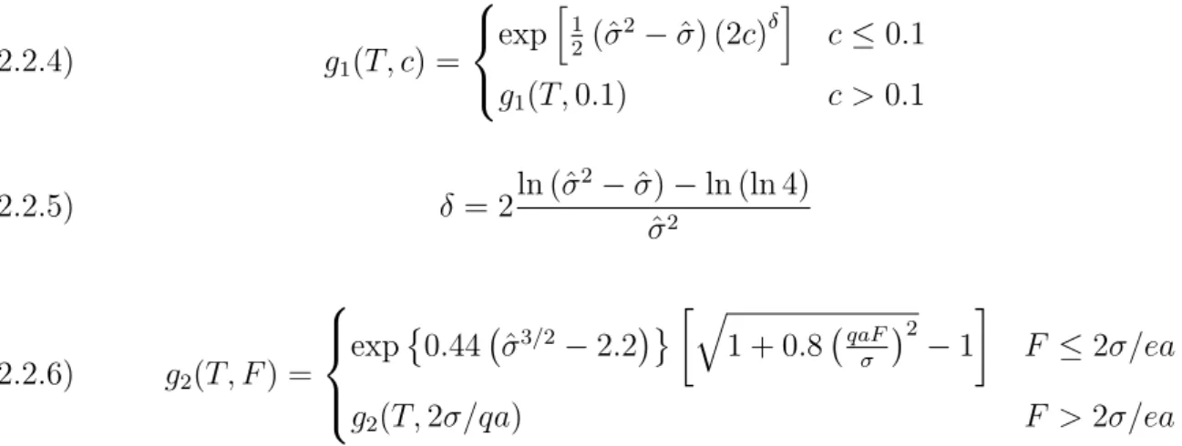
The Gaussian Disorder Model in its basic form assumes that all states are localized on a Cartesian grid. The grid defines sites separated by a distance a; therefore, the total density of states is N0 = a−3. At a given time, each state can be either occupied by charge carrier
or not. State energies are random according to a Gaussian distribution to introduce the diagonal(energetic) disorder. The standard deviation σ of such a Gaussian density-of-states is simply called disorder. For convenience, normalized disorder is introduced, defined as (2.1.1) σ = σ/kˆ BT
. Practical values of disorder are in between 50meV and 150meV . At room temperature, that corresponds approximately to a 3 ≤ ˆσ ≤ 6 normalized disorder


![Figure 1.8.2. Stationary space-charge-limited current-voltage characteristics and fits with dif- dif-ferent models, from reference [39].](https://thumb-eu.123doks.com/thumbv2/123doknet/14718866.750775/38.892.250.672.559.873/figure-stationary-charge-limited-current-voltage-characteristics-reference.webp)


![Figure 2.3.1. Inverse Einstein relation in Gaussian density of states. After [46]..](https://thumb-eu.123doks.com/thumbv2/123doknet/14718866.750775/48.892.204.718.148.509/figure-inverse-einstein-relation-gaussian-density-states.webp)
![Figure 2.3.2. Diffusion enhancement factor in extended Gaussian disorder model. After [46].](https://thumb-eu.123doks.com/thumbv2/123doknet/14718866.750775/49.892.203.716.150.507/figure-diffusion-enhancement-factor-extended-gaussian-disorder-after.webp)

