HAL Id: hal-01820977
https://hal.archives-ouvertes.fr/hal-01820977
Submitted on 22 Jun 2018
HAL is a multi-disciplinary open access
archive for the deposit and dissemination of
sci-entific research documents, whether they are
pub-lished or not. The documents may come from
teaching and research institutions in France or
abroad, or from public or private research centers.
L’archive ouverte pluridisciplinaire HAL, est
destinée au dépôt et à la diffusion de documents
scientifiques de niveau recherche, publiés ou non,
émanant des établissements d’enseignement et de
recherche français ou étrangers, des laboratoires
publics ou privés.
studied by Laue microdiffraction
Z. Ren, T.W. Cornelius, C. Leclere, A. Davydok, Jean-Sébastien Micha, Odile
Robach, G. Richter, O. Thomas
To cite this version:
Z. Ren, T.W. Cornelius, C. Leclere, A. Davydok, Jean-Sébastien Micha, et al.. Plasticity in
inho-mogeneously strained Au nanowires studied by Laue microdiffraction. MRS Advances, Cambridge
University Press, In press, 3 (39), pp.2331-2339. �10.1557/adv.2018.465�. �hal-01820977�
Plasticity in inhomogeneously strained Au nanowires
studied by Laue microdiffraction
Journal: MRS Advances
Manuscript ID MRSAdv-2018-0072.R1 Manuscript Type: Regular Article
Date Submitted by the Author: n/a
Complete List of Authors: Ren, Zhe; Aix Marseille University, CNRS, IM2NP UMR 7334
Cornelius, Thomas; Aix Marseille University, CNRS, IM2NP UMR 7334 Leclere, Cédric; Aix Marseille University, CNRS, IM2NP UMR 7334 Davydok, Anton; Aix Marseille University, CNRS, IM2NP UMR 7334 Micha, Jean-Sebastien; European Synchrotron Radiation Facility (ESRF), CRG-IF BM32 beamline; CEA
Robach, Odile; European Synchrotron Radiation Facility (ESRF), CRG-IF BM32 beamline; CEA, INAC/MEM
Richter, Gunther; Max-Planck Insitut for Intelligent Systems Thomas, Olivier; AIx Marseille Université, IM2NP
Keywords: nanostructure, x-ray diffraction (XRD), dislocations
Plasticity in inhomogeneously strained Au
nanowires studied by Laue microdiffraction
Z. Ren1, T.W. Cornelius1, C. Leclere1, A. Davydok1, J. -S. Micha2,3, O. Robach2,4, G. Richter5, O. Thomas1
1Aix Marseille Univ, Univ de Toulon, CNRS, IM2NP UMR 7334, 13397 Marseille, France
2CRG-IF BM32 Beamline, European Synchrotron (ESRF), CS40220, 38043 Grenoble Cedex 9, France
3Université Grenoble Alpes, CEA/INAC, UMR CNRS SPrAM, 17 rue des Martyrs, 38054 Grenoble, France
4Université Grenoble Alpes, CEA/INAC/MEM, 17 rue des Martyrs, 38054 Grenoble, France
5Max Planck Institute for Intelligent Systems, Heisenbergstrasse 3, 70569 Stuttgart, Germany
ABSTRACT
Plasticity in as-grown gold nanowires deformed in three-point bending configuration was studied by Laue microdiffraction. One-dimensional orientation maps of the Au crystal along the nanowire were generated from which the deformation profile was inferred. The crystal lattice was found to rotate continuously around the Au [211] direction, which is transverse to
the wire axis evidencing the storage of geometrically necessary dislocations (GNDs). The analysis of the diffraction peak shape points to the activation of multiple slip systems in contrast to the formation of wedge shaped twins predicted by MD simulations.
INTRODUCTION
Micro- and nanomechanical studies have demonstrated that the mechanical behavior at small scales differs from the behavior of bulk materials [1]. Already in the 1950s, Brenner [2] and Herring and Galt [3] showed that microwhsikers exhibit higher
yield strengths than their bulk counterparts. Recent studies on defect scarce nanowires even revealed ultra-high yield strengths reaching the theoretical limit of the material [4]. Most micro- and nano-mechanical tests were performed uniaxially, i.e. by tension or compression tests. During plasticity dislocations glide through the micro- and nanostructures before they can interact with each other in contrast to dislocation interaction at macroscopic scales [5]. Together with the small number of pre-existing dislocations in these small scale structures in their initial state, a high density of stored dislocations after mechanical testing is rarely observed. For example, leading partial dislocations with higher Schmid factors are preferentially generated in tensile tested single-crystalline gold nanowires [6, 7, 8]. They rapidly glide through the nanowire leaving stacking faults behind which accumulate and eventually result in the formation of Σ3 twins.
In contrast to uniaxial tests, bending is more complex inducing strain gradients in the deformed structure. At the micro- and nanoscale the mechanical behaviour of inhomogeneoulsy strained objects is much less studied although it is of major importance for applications in flexible electronics or micro-electromechanical systems. Recent cantilever bending tests on micrometer sized beams that were prepared by FIB milling revealed the storage of geometrically necessary dislocations (GNDs) in contrast to uniaxial tests [9, 10, 11, 12, 13, 14, 15, 16]. However, reports on the plastic behaviour of bent nanostructures are scarce. A recent work describes the elastic behaviour of Au nanowires studied by in situ three point bending test in combination with Laue micro-diffraction but it does not give insight into its plastic deformation [17]. The present work details the plasticity in defect scarce gold nanowires mechanically tested in a three-point bending configuration and characterized by Laue microdiffraction.
The outline of the paper is the following. In section 2, the experimental details of the three-point bending tests are presented. The experimental results for plastically deformed Au nanowires are presented in section 3, while the simplest modeling system used for plane strain bending is revisited and compared to the experimental results in section 4. Finally, in the last section, the results are summarized and conclusions are drawn.
EXPERIMENTAL
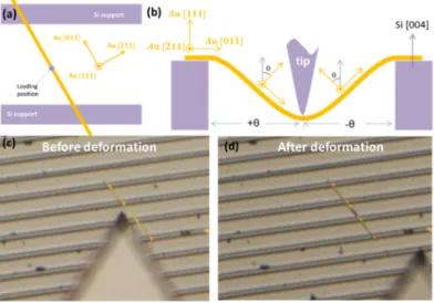
Single-crystalline and nominally defect-free Au nanowires were grown by physical vapor deposition on carbon coated tungsten or molybdenum substrates [4]. After growth, the substrate is scratched across a pre-patterned Si surface, which contains 10 µm wide and 1.5 µm deep micro-trenches prepared by UV lithography and reactive ion etching. Some of the randomly distributed Au nanowires cross Si micro-trenches forming self-suspended nano-bridges. According to previous characterizations, these nanowires grow along the Au [011] direction and typically lie with one of their Au (111) side facets on the Si substrate, as schematically illustrated in Fig. 1(a) and (b) [17]. For avoiding any sliding of the nanowire during mechanical testing, it is firmly clamped to the Si supports by depositing carbon from the residual gas in a SEM chamber.
Fig. 1: Schematic illustration of the crystalline orientation for a gold nanowire crossing a Si micro-trench: (a) Top view and (b) side view. Optical microscopy images of a Au nanowire (c) before and (d) after plastic deformation. Note that the AFM-tip was displaced after the three-point bending test.
Three-point bending tests were performed using a custom-designed atomic force microscope, which has been developed for in-situ nano-mechanical tests on synchrotron beamlines [17, 18, 19]. For alignment, the AFM-tip was firstly placed close to the nanowire using optical microscopy rendering a precision of few micrometers (see Fig. 1(c)). Subsequently, the AFM-tip was positioned above the center of the suspended nanowire part by means of AFM topography images. Once the alignment was finalized, the AFM-tip was lowered, pressing against the nanowire and, thus deflecting it. After a pre-defined displacement, the tip was retracted until it reached its initial position. After deformation, optical microscopy images revealed a darker section along the nanowires which originates from the fact that less light is reflected from the plastically bent part into the microscope objective (see Fig. 1(d)).
The plastically deformed Au nanowires were studied by Laue microdiffraction at the French CRG-IF beamline BM32 at the European Synchrotron ESRF in Grenoble (France). The polychromatic X-ray beam with an effective energy range from 5 to 25 keV was focused down to a size of 400 nm (H) * 500 nm (V) on the sample surface employing a pair of Kirkpatrick-Baez (KB) mirrors [20]. The diffracted X-rays were recorded by a MarCCD165 detector with 2048 * 2048 pixels of 80 µm in size, which were mounted at 90° with respect to the incident beam. The nanowires were located by mapping the Au LIII fluorescence yield employing a Röntec energy dispersive detector. Subsequently, Laue microdiffraction patterns were recorded along the wire in steps of 500 nm. Additional diffraction patterns were recorded 2 µm away from the wire on the bare Si substrate serving as background images.
RESULTS
Scanning electron microscopy images of a Au nanowire (with a width of ~640 nm, a length of ~ 41 µm, and a thickness of 90 nm) before and after loading are presented in Fig. 2(a) and (b), respectively, revealing that the nanowire does not slide
over the Si support during the deformation process. For the following discussion, the nanowire is subdivided into three regions R1, R2, and R3 corresponding to the three trenches crossed by it. The load was applied in the center of R2, while the regions R1 and R3 were left untouched. Near the upper Si support of region R2, slip traces form surface steps with an angle α of about 120° with respect to the growth direction (see Fig. 2(c)), while no such surface steps were found at other parts along the nanowire. Considering the geometry of the nanowire and the calculated Schmid factors, these slip traces correspond to the emission of dislocations on the 111 slip plane.
Fig. 2: SEM image of a gold nanowire (a) before and (b) after plastic deformation. (c) Enlarged view around the break point. d) Deviation angle along the nanowire for the three distinct Au crystalline directions. e) Vertical displacement along the nanowire computed from the bending angles presented in (d).
Laue microdiffraction patterns recorded along the plastically deformed nanowire are indexed with the LaueTools software, from which one-dimensional orientation maps are generated. In the present work, deviation angles for the three distinct Au crystalline directions (Au [111], Au [011] , Au [211] ) were selectively calculated with respect to the reference directions at one end of the nanowire (see Fig. 2(d)). Considering the geometry of the nanowire, these three crystalline directions correspond to the top surface direction, the nanowire growth axis, and the direction perpendicular to the loading plane, respectively. At the positions of the Si supports, which are marked by blue dashed lines, all deviation angles are around 0° indicating that the nanowire remains flat and firmly clamped. While the nanowire was loaded by the
AFM-tip neither in the region R1 nor in R3, the observed deviation angles exhibit different behaviours in these two parts: in R1 the nanowire shows minute deformations with all deviation angles close to 0° while in region R3 the deviation angles for the Au [011] and the Au [111] directions exhibit a sine like variation of up to ±2°. Considering the geometry of the nanowire, this variation corresponds to a bending in the vertical plane, which may be induced by the stress applied in the central region transmitted via the clamping.
In region R2, the loading position is marked by the dashed line in the center of the self-suspended part. At the right-hand side of the loading position, two data points are missing since the diffraction intensity at these measurement positions is at the background level. Comparing the SEM image (see Fig. 2(b)) and the fluorescence map, the missing data points suggest that the nanowire is actually broken at the feature shown in Fig. 2(c). The deviation angles in the vicinity to this position are close to zero indicating that the orientation of the Au crystal is similar to its initial state. Thus, the evidenced slip traces around this position might indicate the sliding of dislocations through the crystal without storage. At the left-hand side of the loading position, the bending angles for the Au [111] and the Au [011] directions exhibit similar continuous variations with a maximum of around 20°. Much smaller angles with values less than 5° are observed for the Au [211] direction. These findings indicate that along the nanowire the Au crystal mainly rotates around the [211] axis being equivalent to a deformation in the vertical plane.
Neglecting deformation caused by dislocations which escaped at the surface, the deviation angle of the Au [111] and Au [011] directions correspond to the bending angle of the nanowire. From the slope of the local deformation, the profile of the complete nanowire is estimated by integrating the local deformations ∆ between adjacent measurement points. The deformation profile obtained after setting the displacements at the two ends of the nanowire to zero is presented in Fig. 2(e). While the nanowire stays almost flat in region R1, a small upward bending of around 80 nm is observed in region R3. In the zone where the nanowire has been mechanically loaded by the AFM-tip, the Au nanowire bends downwards at the left-hand side of the loading position. At the right-hand side of the loading point, the Au nanowire remains flat up to a discontinuity at the breaking point where a height difference of ~ 800 nm is observed.
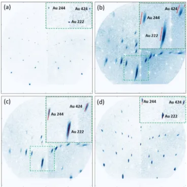
Due to the fact that the Laue microdiffraction experiments were performed after the mechanical deformation, the elastic strain is assumed to be negligible and the found deformations are thus solely attributed to the storage of GNDs. The crystal rotation and nanowire deformation with respect to GNDs is further examined by analyzing the shape of the diffraction peaks. Diffraction patterns recorded at four different positions along the nanowire (marked by arrows in Fig. 2) are presented in Fig. 3. At the reference point, the diffraction pattern consists of sharp and round Laue spots indicating that the non-deformed part of the nanowire is free of stored GNDs (see Fig. 3(a)). In contrast, for the two diffraction patterns (Fig. 3(b) and (c)) recorded at the left-hand side of the loading position in region R2, where the Au crystal exhibits large deviation angles, strongly streaked Laue spots are observed. The direction of the streaking agrees well with the expected elongation directions for the plane strain bending (the rotation around Au [211] axis), which are marked by red lines in the inset of the figures. This supports the former observation that the nanowire mainly deforms by bending in the vertical plane which can be simply accommodated by the [011] 111 type of dislocations. However, the slight deviation of the predicted peak positions and the significant broadening of the diffraction peaks both indicate that the rotation around the Au [211] axis is caused by the simultaneous activation of multiple slip systems. In the diffraction pattern recorded near the rupture of the nanowire (Fig. 3(d)), the Laue spots are at similar positions on the detector as for the reference diffraction pattern (Fig. 3(a)) revealing that this nanowire
part has a similar crystalline orientation as the non-deformed part. However, the slight streaking of the diffraction peaks indicates that this section of the nanowire is not defect-free.
Fig. 3: Laue microdiffraction patterns taken (a) at the reference position (Y= 4.4 µm), b) at the left-hand side and c) at the right-hand side of the largest bending angle (Y= 16.4, 17.4 µm), and (d) at the right-hand side of the loading position (Y=19.9 µm). The positions where these diffraction patterns were recorded are indicated by arrows in Figs. 2(b) and (d).
DISCUSSION
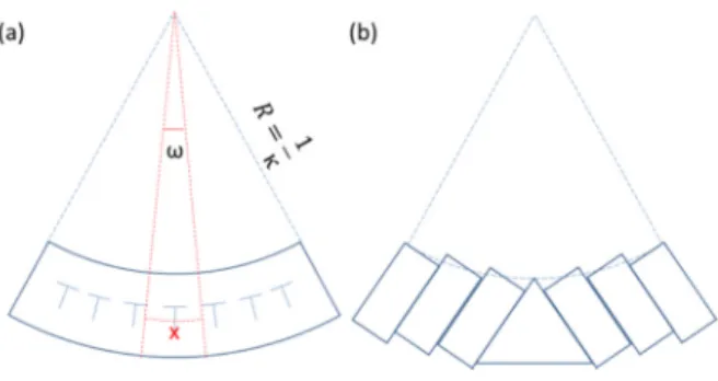
To accommodate deformation in a structure, geometrically necessary dislocations are stored in the material where the dislocation density depends on the activated slip systems [21]. In the case of plane strain bending, the simplest and most energy efficient configuration is the storage of polarized edge dislocations oriented perpendicular to the bending plane with the slip plane being parallel to the top surface of the beam and the Burgers vector directed along the beam axis (Fig. 4(a)) [ 22 ]. Considering the Au crystalline orientation introduced in Fig. 1, in this experiment bending should be solely accommodated by the storage of [011] 111 type edge dislocations. At variance with this simplified case, a similar bending geometry may be obtained by a shearing process where dislocations glide through the structure without causing a rotation of the crystalline lattice leaving slip traces on the sample surface (Fig. 4(b)). Some recent MD simulations [23, 24] even suggest that at the nano-scale bending may be accommodated by the formation of wedge-shaped twins similar to the ones observed in uniaxial tension tests. These wedge-shaped twins are localized in the center of the nanowire, and completely vanish upon the unloading leaving the nanowire almost free of defects.
Fig. 4: Schematic views a) of the plane strain bending with the minimum stored energy, where the red lines mark the two neighboring measurement positions and b) of the bending geometry achieved via shearing processes.
Our experimental findings, which show a continuous variation of the lattice orientation, suggests that at 100 nm scale bending is still caused by the storage of GNDs. The differences between the experiment and the models may be attributed to the nucleation process, which plays an important role in the deformation of nanomaterials. Regarding the Schmid factors for the pure bending test (see table 1), which define the preferentially activated slip systems, the activation of the of [011] 111 slip systems is not geometrically favored. Thus, the measured slip system is different compared to the case illustrated in Fig. 4(a). Besides, the reported nanowire deformation shows a deviation from the vertical plane, that may be attributed to a torsion along the nanowire which is probably caused either by the fact that the nanowire is not lying perpendicular to the Si supports or by a misalignment of the AFM-tip with respect to the center of the nanowire. Such kind of torsion affects the stress distribution along the nanowire yielding a stress on the (111) planes which are in zone with the nanowire axis, thus activating the type of edge dislocations indicated by the experimental findings. While the MD simulated bending test is achieved by applying a rotation moment at both ends of the nanowire, actual three-point bending tests contain points of stress concentrations at the loading position and at the clamping, which play an important role in the dislocation nucleation process. Consequently, in situ experiments are necessary to characterize the deformation profile during three-point bending tests and provides additional information on the nucleation of the dislocations. In fact, three-point bending tests using the same AFM as in the present work coupled with Laue microdiffraction were successfully performed and are the topic of another publication [25].
Table 1: Schmid factors calculated for the tensile side of the nanowire (tensile axis along Au [011] direction) and the rotation axis of edge dislocations for different slip systems
Slip plane [111] [111] [111] [111] Burger’s
vector [011] [101] [110] [011] [101] [110] [011] [101] [110] [011] [101] [110] Schmid
CONCLUSION
In the present work, the plasticity of inhomogeneously strained Au nanowires tested in a three-point configuration was investigated by Laue microdiffraction. One-dimensional orientation maps of the Au nanowire obtained from diffraction patterns recorded all along the deformed nanowire revealed a continuous rotation of the crystal lattice which evidences the storage of GNDs to accommodate the plastic deformation. Peak shape analysis of the Laue diffraction spots indicates the activation of multiple slip systems. These findings are in contrast with recent MD simulations which suggest the formation of wedge shape twins that disappear upon unloading leaving an almost perfect nanowire behind. The difference between the simulation and our experimental findings are probably related to the nucleation process of the dislocations within the specimen.
ACKNOWLEDGEMENTS
The authors gratefully acknowledge the financial support from the French National Research Agency through the project ANR-11-BS10-01401 MecaniX. They further thank the French CRG program committee for the allocated beamtime at the BM32 beamline at ESRF. They also thank E. Bitzek from the Friedrich-Alexander University Erlangen-Nürnberg for fruitful discussions.
References
[1] Uchic, M.D., et al., Sample Dimensions Influence Strength and Crystal Plasticity. Science, 2004. 305(5686): p. 986-989.
[2] Brenner, S.S., Tensile strength of whiskers, J. Appl. Phys. (1956) 27, p. 1484-1491 [3] Herring, C. and J.K. Galt, Elastic and Plastic Properties of Very Small Metal Specimens.
Physical Review, 1952. 85(6): p. 1060-1061.
[4] Richter G., Hillerich K., Gianola D.S., Mönig R., Kraft O., Volkert C.A., Ultrahigh Strength Single Crystalline Nanowhiskers Grown by Physical Vapor Deposition. Nano Letters, 2009. 9(8): p. 3048-3052.
[5] Oh, S.H., Legros M. Kiener D., Dehm G., In situ observation of dislocation nucleation and escape in a submicrometre aluminium single crystal. Nat Mater, 2009. 8(2): p. 95-100. [6] Lee, S., Im J., Yoo Y., Bitzek E., Kiener D., Richter G., Kim B., Oh S.H., Reversible cyclic
deformation mechanism of gold nanowires by twinning–detwinning transition evidenced from in situ TEM. Nat Commun, 2014, 5.
[7] Roos, B., Kapelle B., Richter G., Volkert C.A., Surface dislocation nucleation controlled deformation of Au nanowires. Applied Physics Letters, 2014. 105(20): p. 201908. [8] Sedlmayr, A., Bitzek E., Gianola D.S., Richter G., Mönig R., Kraft O., Existence of two
twinning-mediated plastic deformation modes in Au nanowhiskers. Acta Materialia, 2012. 60(9): p. 3985-3993
[9] Demir, E. and D. Raabe, Mechanical and microstructural single-crystal Bauschinger effects: Observation of reversible plasticity in copper during bending. Acta Materialia, 2010. 58(18): p. 6055-6063.
[10] Demir, E., D. Raabe, and F. Roters, The mechanical size effect as a mean-field breakdown phenomenon: Example of microscale single crystal beam bending. Acta Materialia, 2010. 58(5): p. 1876-1886.
[11] Demir, E., F. Roters, and D. Raabe, Bending of single crystal microcantilever beams of cube orientation: Finite element model and experiments. Journal of the Mechanics and Physics of Solids, 2010. 58(10): p. 1599-1612.
[12] Gong, J., Birtton T.B., Cuddihy M.A., Dunne F.P.E., Wilkinson A.J.,〈a〉 Prismatic, 〈a〉 basal, and 〈c+a〉 slip strengths of commercially pure Zr by micro-cantilever tests. Acta Materialia, 2015. 96: p. 249-257.
[13] Kiener, D., Motz C., Grosinger W., Weygand D., Pippan R., Cyclic response of copper single crystal micro-beams. Scripta Materialia, 2010. 63(5): p. 500-503.
[14] Kirchlechner, C., Grosinger W., Kapp M.W., Imrich P.J., Micha J.-S., Ulrich O., Keckes J., Dehm G., Motz C., Investigation of reversible plasticity in a micron-sized, single crystalline copper bending beam by X-ray µLaue diffraction. Philosophical Magazine, 2012. 92(25-27): p. 3231-3242.
[15] Konijnenberg, P.J., S. Zaefferer, and D. Raabe, Assessment of geometrically necessary dislocation levels derived by 3D EBSD. Acta Materialia, 2015. 99: p. 402-414. [16] Motz, C., T. Schöberl, and R. Pippan, Mechanical properties of micro-sized copper bending
beams machined by the focused ion beam technique. Acta Materialia, 2005. 53(15): 4269-4279.
[17] Leclere, C., Cornelius T.W., Ren Z., Robach O., Micha J.-S., Davydok A., Ulrich O., Richter G., Thomas O., In situ bending of an Au nanowire monitored by micro Laue diffraction. Journal of Applied Crystallography, 2015. 48(1): p. 291-296.
[18] Leclere, C., Cornelius T.W., Ren Z., Davydok A., Micha J.-S., Robach O., Richter G., Belliard L., Thomas O., KB scanning of X-ray beam for Laue microdiffraction on accelero-phobic sample. Journal of Synchrotron Radiation, 2016. 23 (6): p. 1395-1400. [19] Ren, Z., Mastropietro F., Davydok A., Langlais S., Richard M.-I., Furter J.-J., Thomas O.,
Dupraz M., Verdier M., Beutier G., Boesecke P., Cornelius T.W., Scanning force microscope for in situ nanofocused X-ray diffraction studies. Journal of Synchrotron Radiation, 2014. 21(5): p. 1128-1133.
[20] Ulrich O., Biquard X., Bleuet P., Geaymond O., Gergaud P., Micha J.-S., Robach O., Rieutord F., A new white beam x-ray microdiffraction setup on the BM32 beamline at the European Synchrotron Radiation Facility, Rev. Sci. Instrum. 82 (2011) 033908 [21] Fleck, N.A., et al., Strain gradient plasticity: Theory and experiment. Acta Metallurgica et
Materialia, 1994. 42(2): p. 475-487.
[22] Gao, H., et al., Mechanism-based strain gradient plasticity— I. Theory. Journal of the Mechanics and Physics of Solids, 1999. 47(6): p. 1239-1263.
[23] Nöhring, W.G., Möller J.J., Xie Z., Bitzek E., Wedge-shaped twins and pseudoelasticity in fcc metallic nanowires under bending. Extreme Mechanics Letters.
[24] Zheng, Y.G., Zhang H.W., Chen Z., Wang L., Zhang Z.Q., Wang J.B., Formation of two conjoint fivefold deformation twins in copper nanowires with molecular dynamics simulation. Applied Physics Letters, 2008. 92(4): p. 041913.
[25] Ren Z., Cornelius T.W., Leclere C., Davydok A., Micha J.-S., Robach O., Ullrich O., Richter G., Thomas O., Three-point bending behavior of Au nanowires studied by in situ Laue microdiffraction, submitted