HAL Id: tel-02946584
https://tel.archives-ouvertes.fr/tel-02946584
Submitted on 23 Sep 2020HAL is a multi-disciplinary open access archive for the deposit and dissemination of sci-entific research documents, whether they are pub-lished or not. The documents may come from teaching and research institutions in France or abroad, or from public or private research centers.
L’archive ouverte pluridisciplinaire HAL, est destinée au dépôt et à la diffusion de documents scientifiques de niveau recherche, publiés ou non, émanant des établissements d’enseignement et de recherche français ou étrangers, des laboratoires publics ou privés.
quantum conductors
Everton Arrighi
To cite this version:
Everton Arrighi. Time-resolved measurements of collective effects in quantum conductors. Mesoscopic Systems and Quantum Hall Effect [cond-mat.mes-hall]. Université Grenoble Alpes [2020-..], 2020. English. �NNT : 2020GRALY001�. �tel-02946584�
THÈSE
Pour obtenir le grade de
DOCTEUR
DE L'UNIVERSITÉ GRENOBLE ALPES
Spécialité : Nanophysique
Arrêté ministériel : 25 mai 2016
Présentée par
Everton
Arrighi
Thèse dirigée par Christopher Bäuerle
préparée au sein Laboratoire Institut Néel - CNRS et de l’École doctorale de Physique
Time-resolved
measurements of
collective
effects in quantum
conductors
Thèse soutenue publiquement le 7 février 2020, devant le jury composé de :
Gwendal Fève
Professeur, LPENS, Sorbonne Université, Rapporteur
Masaya Kataoka
Principal Research scientist, National Physical Laboratory, Rapporteur
Anne Anthore
Maîtresse de conférence, C2N-CNRS, Université Paris Diderot, Examinatrice
Serge Florens
Directeurs de recherche, Institut Néel-CNRS, Communauté Université Grenoble Alpes, Président
Xavier Waintal
Directeur de recherche, IRIG-CEA Grenoble, Examinateur
Christopher Bäuerle
Directeur de recherche, Institut Néel-CNRS, Communauté Université Grenoble Alpes, Directeur de thèse
Abstract
Quantum dynamics is very sensitive to dimensionality. While two-dimensional electronic systems form Fermi liquids, one-dimensional systems – Tomonaga–Luttinger liquids – are described by purely bosonic excitations, even though they are initially made of fermions. With the advent of coherent single-electron sources, the quantum dynamics of such a liquid is now accessible at the single-electron level.
In this PhD work, we study the most general case where the system can be tuned continuously from a clean one-channel Tomonaga–Luttinger liquid to a multi-channel Fermi liquid in a non-chiral system. We use time-resolved measurement techniques to determine the time of flight of a single-electron voltage pulse and extract the collective charge excitation velocity. Analysing the propagation velocity allows to reveal the collective effects that govern the physics in our quasi one-dimensional system. Our detailed modelling of the electrostatics of the sample allows us to construct and understand the excitations of the system in a parameter-free theory. We show that our self-consistent calculations capture well the results of the measurements, validating the construction of the bosonic collective modes from the fermionic degrees of freedom.
The presented time control of single-electron pulses at the picosecond level will also be important for the implementation of waveguide architectures for flying qubits using single electrons. Integrating a leviton source into a waveguide interferometer would allow to realise single-electron flying qubit architectures similar to those employed in linear quantum optics. Furthermore, our studies pave the way for studying real-time dynamics of a quantum nanoelectronic device such as the measurement of the time spreading or the charge fractionalisation dynamics of the electron wave packet during propagation.
Contents
1 Introduction 1
1.1 Quantum optics . . . 2
1.2 Electron quantum optics . . . 2
1.3 Two-Dimensional electron gas . . . 3
1.4 Quantization of conductance . . . 4
1.5 Quantum Hall effect . . . 5
1.5.1 Electronic Mach-Zehnder interferometer . . . 6
1.6 Flying qubits . . . 7
1.7 Single electron sources . . . 8
1.7.1 Controlled emission of single-electron in a dynamic quantum dot . . . 9
1.7.2 An on-demand coherent single-electron source . . . 10
1.7.3 Moving quantum dot as a single-electron source . . . 10
1.7.4 Leviton source . . . 12
1.7.5 Manipulation of the quantum state of a flying electron . . . 16
1.8 Detection of a flying-electron . . . 21
1.9 Characterization of the velocity of a voltage pulse in an interacting system . 23 1.9.1 Single electron tunnelling experiments . . . 23
1.9.2 Time-resolved measurements . . . 25
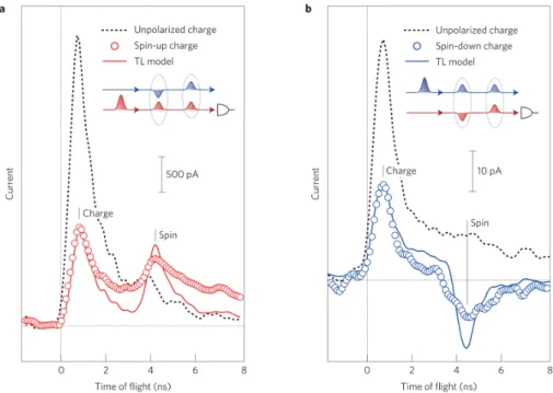
Separation of the charge mode and neutral mode . . . 26
1.10 Conclusion . . . 30
2 Plasmon theory 31 2.1 Electrostatic problem . . . 32
2.2 Quasi-1D problem . . . 35
2.3 Conclusion . . . 39
3 Experimental set-up and technical specifications 41 3.1 Characterising the dynamics of a Voltage pulse in a coherent quantum conductor . . . 42
3.2 Determining the coherence of a quantum conductor at zero magnetic field . 43 3.3 Sample fabrication . . . 44 3.4 Experimental set-up . . . 46 3.4.1 Cold finger . . . 46 3.4.2 Chip carrier . . . 46 3.4.3 Electronic set-up . . . 48 DC lines . . . 48 iii
Control of the Schottky gates . . . 49
RF lines . . . 51
Creation of fast pulses . . . 53
Pulse box . . . 56
Inducing an excitation with a capacitively coupled gate . . . 60
Homodyne detection . . . 65
3.5 Time-resolved measurements . . . 66
QPC as a fast switch . . . 67
Simulating the measured signal . . . 69
3.5.1 Time calibration - what do we need to know? . . . 71
Time calibration: Reflectometry . . . 71
Time calibration: in-situ . . . 73
Time-resolved measurements varying the excitation number . . . 73
3.6 Conclusion . . . 74
4 Experimental results 75 4.1 Time-of-flight measurements . . . 75
4.2 Measurements of the Plasmon velocity . . . 79
4.2.1 Amplitude dependence . . . 79
4.2.2 Confinement dependence . . . 80
4.2.3 Generation and TOF measurements of a Lorentzian pulse . . . 83
4.3 Simulating the plasmon velocity . . . 85
4.4 Velocity control via QPC selection . . . 87
4.4.1 Modelling the effect of the QPC . . . 92
Funnelling scenario . . . 92
Filtering scenario . . . 93
Time evolution of the electron excitation – Studying the relaxation length . . . 98
Determination of the propagation velocity from an electronic cavity . 101 4.5 Conclusion . . . 104
5 Summary and Outlook 107
Appendix 109
A Lock-in measurements 109
B Derivation of the transmission matrix for the tunnel-coupling wire 111
C Old cold finger 115
D Time-resolved sinusoidal signals 117
Contents v
F Fitting parameters of a electron cavity 121
G Using the QPC to create short pulses 123
H Impedance mismatch 129
I Transmission of the DC lines 131
J Transmission of the RF lines 133
Bibliography 135
CHAPTER
1
Introduction
The beginning of the 20th century was a prosperous period when it comes to progress in science, inventions and technology. However, many of the ideas were not believed to be possible at the end of the previous century. An example is a famous statement from Lord Kelvin: "Heavier-than-air flying machines are impossible" [1] in 1895. One year later, he said: "I have not the smallest molecule of faith in aerial navigation other than ballooning" [1]. Despite the lack of faith from Lord Kelvin, the Brazilian Albert Santos-Dumont realized the first public demonstration of a powered, heavier-than-air aircraft in 1906 at the Bagatelle field [2]1. More than a hundred years later, there are not as many balloons
as aeroplanes in the sky.
Lord Kelvin shared his "optimism" also about physics. In 1900, he stated "There is nothing new to be discovered in physics now. All that remains is more and more precise measurements" [1]. The one who had a similar opinion was Philipp Von Jolly, a physicist and mathematician, professor at the University of Munich. He advised one of his students not to go into physics, saying: "In this field, almost everything is already discovered, and all the remains is to fill a few unimportant holes" [4]. This quote dates from 1878 and it ends up as a big destiny’s irony because the student that he had advised was Max Planck, whose work is at the origin of the field of quantum theory.
In 1901, to solve the ultraviolet catastrophe problem [5], Planck considered that the black-body radiation is emitted in discrete energy packets named quanta, recovering the corpuscular theory of light proposed by Newton. Further studies have followed Planck’s approach, such as the study from Albert Einstein explaining the photoelectric effect in 1905, for which he got the Nobel Prize in 1921.
Proper treatment of the quantization of the light came in 1927, with a seminal work from Paul Dirac of the quantum theory of radiation [6]. Roy J. Glauber, Leonard Madel and George Sudarshan have made use of the quantum theory to the electromagnetic field in the ’50s and ’60s, achieving a better understanding of the statistics of light [7]. They have created several important concepts such as coherent states. It was predicted that quantum states of light with features different from classical states, such as squeezed light.
1 The flight of the 14-Bis (Dumont’s aeroplane) was the first aviation activity to be homologated by the Fédération aéronautique internationale (FAI), with self-propelled take-off. Years later, it was recognized by the FAI that the Wright brothers had accomplished this feat in 1905. The FAI recognizes the first flight happened in 1903. However, the Wright brothers’ aeroplane did not have a self-propelled take-off at the time. It might be that the french Clément Ader achieved the self-propelled take-off in 1890, at the south-west of Paris. Nevertheless, the only witnesses were his employees [3].
This field that deals with the phenomena that cannot be understood by considering light as an electromagnetic wave is called quantum optics. The light is treated as a stream of photons (quanta of light).
1.1 Quantum optics
A milestone in quantum optics happened in 1956, with the work of Hanbury Brown and Twiss [8]. Their experiment consisted in measuring the correlation in the light intensities received by two detectors, of a light source split by a half-silvered mirror. They have observed positive correlation between the light beams, and their scheme become a famous experiment to test the statistics of particles. Furthermore, the confirmation of non-classical properties of light was given by Kimble, Dagenais and Mandel measuring the photon anti-bunching [9]. This work developed the first single-photon source.
Quantum optics was also useful in clarifying the mysteries of quantum mechanics. A work from Einstein, Podolsky and Rosen raised the possibility that quantum mechanics was not complete [10], and it was proposed the existence of local hidden-variables to explain the behaviour of entanglement. Based on correlations, Bell derived an inequality that could bring to a conclusion about the existence of local-variables [11]. In 1981, with the help of quantum optics, the violation of Bell’s inequality was measured for the first time [12], discarding the possibility of hidden-local variables in quantum mechanics.
The subject of quantum optics has become a vast field and is now related to subjects that go from quantum information processing to the study of light-matter interactions [13]. Despite all the famous effects of quantum mechanics unveiled with quantum optics experiments, as photons are bosons, it is very difficult to make them interact.
Electrons, which are fermions, are strongly interacting particles due to the existing Coulomb interaction. One could also think to probe the statistics of electrons, with the experiments realised with photons. The possibility to create single electrons on-demand and to investigate such physics with electrons instead of photons opened up an entirely new field often referred to as electron quantum optics.
1.2 Electron quantum optics
Recent advances in nanofabrication and measurement techniques have made it possible to be able to control and manipulate single electrons. These advances allowed envisioning quantum-optics-like experiments with single electrons. This field is still in its infancy, even though a few pioneering experiments have been realised over the last decade. With faster and faster time control of the electron wave packet, such an approach should also allow to use single electrons to implement flying qubit architectures.
In this section, we will describe the building blocks needed to perform the electron coun-terpart of quantum optics. First, we describe the basics of high mobility two-dimensional electron gases (2DEG) based on a GaAs/AlGaAs heterostructure, which are the workhorse of our studies and we review very briefly the main discoveries which have been made with such systems.
Then we review some recent advances in the field of electronic quantum-optics. In particular, we discuss the different single-electron sources that have been developed, giving
1.3 Two-Dimensional electron gas 3
particular emphasis to the Leviton source. In the last part, we review the different methods used to characterise the propagation velocity of electrons in semiconductors.
1.3 Two-Dimensional electron gas
To investigate electronics properties, we use AlGaAs/GaAs heterostructures. These two semiconductors have different energy band gaps (energy separation between the valence band and conduction band). Donors are introduced on the AlGaAs layer, which is represented in figure 1.1a as n-AlGaAs. The electrons diffuse from the n-AlGaAs to the lower energy GaAs layer, leaving positively charged donors at the n-AlGaAs which is balanced by the electrons confined at the heterointercace. Due to the electrostatic potential generated, the band bends as shown in figure 1.1b and a triangular well is formed. The electron energies are increased due to the small space where the electrons are confined, around 8 nm [14]. Thus discrete quantum-electric subbands are formed. At low temperatures, only the first level (subband) is occupied, since the gap energy between the first and the second level (subband) is on the order of 300 K [15–17]. The dopant layer is put at a relatively far distance (40 nm) from the interface of AlGaAs, to avoid any scattering between the donors with electrons in the 2DEG, which helps to achieve high mobility. The density of electrons for the 2DEG used in our experiments is 𝑛𝑠 = 2.11 × 10⁻¹¹cm−2 and the
mobility is of 𝜇 = 1.89 × 106cm2V−1s−1, measured in dark and at 4.2 K. The high-mobility
heterostructures used during my thesis were grown by molecular beam epitaxy, allowing to reach very clean and stable structures. They were provided by our collaborator Prof. Andreas Wieck from the University of Bochum.
E0 E1 + undoped doped EC EV EF GaAs AlGaAs 1261 nm GaAs GaAs 7.5 nm n-AlGaAs 43 nm AlGaAs 89 nm Z 2DEG a b Z +++
Figure 1.1: 2DEG and band structure. a,Vertical cut of the AlGaAs/GaAs
heterostruc-ture used in this thesis. b, Qualitative drawing of the energy of valance band and conduction band along the vertical growth direction. A triangular quantum well is formed at the interface between AlGaAs and GaAs. Figure adapted from [17] and [14].
we can estimate the mean free path from [18]: 𝐿𝑚= ~𝜇
| 𝑒 | √
2𝜋𝑛𝑠 ≈14 µm (1.1)
Another relevant length scale is the coherence length 𝑙𝜑. It corresponds to the length over
which the phase of the electron wave function stays well defined. At low temperature this length is typically of the order of a few tens µm [19–21]. More recently this length-scale has been pushed to more than 100 µm [22] by careful engineering of the quantum device. Thanks to sophisticated nanofabrication techniques we can engineer quantum interferometers by gate patterning of the heterostructure that are smaller than the coherence length in the 2DEG.
Using electron beam lithography it is possible to create the desired quantum circuit. This can be done by depositing metallic gates on the surface of the heterostructure. There is a Schottky barrier at the metal-semiconductor interface, which allows to apply a negative voltage to the metallic gates without having current flowing to the 2DEG. In fact, this negative voltage will deplete the electrons underneath the surface gate, that means we can design and engineer a quantum circuit by simply changing the shape of the gates on the top of the sample. With present state-of-the-art equipment, we can fabricate gates in the order of tens of nanometers. To perform transport measurements, we add ohmic contacts to the 2DEG, such that we can apply a voltage and collect the current going through.
1.4 Quantization of conductance
Mesoscopic physics is the domain that lies between the microscopic and the macroscopic world. With the invention of the two-dimensional electron gas [23], we have a convenient tool to investigate the behaviour of electrons in the mesoscopic regime. One pioneering experiment in this field was the discovery of the quantization of the conductance. The first measurements of this effect were done by B.J. van Wees et al. in Delft [24] and almost at the same time by Wharam et al. [25] at the University of Cambridge. To observe quantized conductance one deposits two metallic Schottky gates in a split geometry (see inset of Figure1.2) and applies a bias voltage to the Ohmic contact in order to pass a current going through the 2DEG. Increasing the negative voltage on these two gates, it is possible to deplete more and more the electrons underneath, arriving at a situation where the width of the slit is on the same order as the Fermi wavelength. This results in the occurrence of plateaus of conductance as a function of the applied gate voltage, as shown in figure1.2.
The constriction created by the two gates on the 2DEG makes that the electron wave functions form 1D subbands. Ideally, the total conductance depends only on the number of available channels in the QPC region. By treating each subband as an independent 1D system, the density of states is simply the sum of the density of states for each subband [26]. The conductance for a one-dimensional ballistic system under an applied bias can be derived by calculating the current flow, which is proportional to the density of states times the velocity. For one-dimensional system, the density of states times the velocity gives a constant, which implies that the conductance is quantized and equal to 2𝑒2/ℎ[26,
1.5 Quantum Hall effect 5
magnetic field [25].
Figure 1.2: Quantization of conductance. The conductance of the Quantum point contact
versus the applied gate voltage. One observes plateaus of conductance with multiples of 2.𝑒2/ℎ. Figure adapted from [24].
The design of the Schottky gates shown in the inset of the figure 1.2 is known as a quantum point contact (QPC), and we will describe several applications using this gate structure. One of these applications is to build a beam splitter since we can set the transmission simply by changing the gate voltages applied to the Schottky gates. Thus we can set the values to one plateau of conductance (full transmission of one channel of conductance) or half of this value (one channel being transmitted with 50% of probability).
Implementing such beam splitters allowed the realization of different quantum interfer-ometers, such as the Young’s double-slit [28], Mach-Zehnder [29,30] or Hong-Ou-Mandel interferometer [31] with electrons.
1.5 Quantum Hall effect
Another breakthrough experiment in the field of mesoscopic physics has been the observation of the Quantum Hall Effect (QHE) by V. Klitzing, Dorda and Pepper in 1980 [32]. Measuring the Hall voltage of a two-dimensional electron gas at liquid helium temperatures and under a high magnetic field, they were the first to measure the quantisation in the Hall resistance.
To explain this effect semi-classically, we can think that by applying a very high magnetic field, the electrons in the bulk start to follow a circular motion due to the Lorentz force, and they form closed trajectories, which is known as cyclotron motion. Thus the electrons in the bulk do not participate to the transport. However, the electrons close to the edges are forced on skipping orbits and only the edge will contribute to the transport. The chirality imposed by the magnetic field makes the electrons that are propagating in opposite edges
travel in opposed direction.
By changing the magnetic field, one can achieve a situation where there are quantised levels of conductance flowing along the edge of the sample and contributing actively to the transport. The number of these edge channels is usually related to the filling factor 𝜈. It can take integer values, and one usually refers to the integer quantum Hall effect (IQHE) while for very high purity samples, fractional numbers can be attained, known as the fractional quantum Hall effect [33]. Here we will not go in further details of the QHE, because all the experiments of my thesis were taken at zero magnetic field. For further details, we address the reader to the following references [18,34].
The edge channels have the remarkable property that backscattering is strongly sup-pressed [35] due to the chirality of the system. This makes it possible to reach a long coherence length of several tens of µm [19–21] and it has been shown that with a smart design it is possible to keep the coherence for more than 200 µm [22].
1.5.1 Electronic Mach-Zehnder interferometer
We described so far how to build an electronic beam splitter and how one can make the electrons propagate along edge channels.
Let us now discuss some experiments made with these tools. The optical Mach-Zehnder interferometer (MZI) is the device that first allowed to demonstrate the phase shift between two optical beams, due to the change in the path length of one of the beams. In figure 1.3a, we show a schematic drawing of the optical interferometer. S stands for the optical source, and then the beam is split in two at beam splitter 1 (BS1). The beams propagate in separated paths, and are recombined in beam splitter BS2. They are then collected at the detector D1 and D2. D1 measures maximum (zero) signal and D2 measures zero (maximum) signal depending whether the phase difference is 0 (𝜋) between the two beams. The sum of the measured signals is equal to the input signal if there is no loss on propagation.
The first Mach-Zehnder interferometer that used as a guide for the electrons an edge channel and as beam splitters QPCs, has been realized by the Weizmann team in 2003 [29]. In figure1.3, we can see the schematic of the experiment, where a magnetic field is applied such that there is only one edge channel (𝜈 = 1).
Similar to the optical counterpart, we have conservation of the current injected in the source leading to 𝐼S = 𝐼D1+ 𝐼D2. Considering the probabilities of transmission and
reflection on the QPC as |𝑟𝑖|2+ |𝑡𝑖|2 = 1, and considering the phase difference between
the two interfering path as 𝜙, the current is then given by 𝐼D1∝ 𝑇D1= |𝑡1.𝑡2|2+ |𝑟1.𝑟2|2+ 2 |𝑡1.𝑡2.𝑟1.𝑟2|cos(𝜙).
To modify the relative phase 𝜙 between the two different paths, one can explore the Aharonov-Bohm effect, which is a spectacular and fundamental phenomenon of quantum mechanics. The electrons will pick a phase corresponding to the magnetic flux going through the area formed by the two different paths. This originates from the coupling between the vector potential and the complex phase in the wavefunction of the electrons. Thus, by varying the magnetic field, one can control the phase difference between the electrons in the different arms, as displayed in figure1.3c. The phase difference between the electrons passing through the two branches induced by the AB effect is equal to:
1.6 Flying qubits 7
Figure 1.3: Optical MZI interferometer and the electronic analogue. a, Schematic
of an optical Mach-Zehnder interferometer, where S is the source, BS1 and BS2 are the beam-splitters, M1 and M2 are mirrors, and D1 and D2 are detectors. b, The electronic version of the MZI, where S in an ohmic contact, to inject current into the 2DEG, the QPCs act as beam splitters, the edge channel works as the waveguide for the electrons, MG1 and MG2 are two Schottky gates that can be used as phase shifters, D1 and D2 are also ohmic contacts, the first placed there to collect current and the second is connected to the ground, to avoid that electron scattered at the second beam splitter interact with electrons entering in the interferometer. c, Plot of the current measured in D1, varying the phase 𝜙 between the different paths in two different ways: with the magnetic field (AB effect) or with the Schottky gate. Figure adapted from [29].
𝛥𝜙= 𝑒𝐵𝐴
~ (1.2)
Where 𝑒 is the elementary charge, 𝐵 is the magnetic field, and 𝐴 is the area enclosed by the two different arms. It is also possible to control the phase by altering the electron path. This can be done by applying a negative gate voltage to one of the surface gates MG1 and MG2. This will induce an increase of the length of the electron path of the lower interferometer branch, as depicted in figure 1.3b by MG1 and MG2.
In reference [29], the authors have controlled the phase between the two arms using the gate and the magnetic field, as presented in figure 1.3c. One observes similar current oscillations for both types of control. From the oscillation amplitude, one can determine the visibility which is defined as 𝜈 = 𝐼𝑚𝑎𝑥−𝐼𝑚𝑖𝑛
𝐼𝑚𝑎𝑥+𝐼𝑚𝑖𝑛. From measuring its dependence on different parameters (temperature, interferometer size, bias etc.) one can quantify the coherence length of the system. For the case of reference [29], with an electronic temperature of 20 mK they have obtained a visibility of 60%. They observed a decrease in visibility when they increased the bias. The same effect is detected with temperature. A direct way to determine the coherence length is by changing the size of the interferometer. This has been done in reference [19] and a coherence length of 𝑙𝜙∼20 µm at 20 mK has been obtained. 1.6 Flying qubits
The ultimate goal of our research is to realize electronic flying qubits using single-electron wave packets. This requires efficient single-electron sources, quantum interferometers to manipulate the quantum state of the propagating electron and a single-electron detector.
Besides building a flying qubit, it is essential to understand first the propagation of a single-electron wave packet, and this has been the central part of this PhD work.
The flying qubit has some intrinsic advantages over static qubits in its architecture. First, we can create entangled states on the flight and separate them afterwards, thus with this architecture, the transferring of entangled states from different places appears naturally. Second, ideally one would be able to decouple the hardware with the number of qubits, being able to create qubits on-demand, without the need to add new devices. For this purpose, we could follow the proposal described in [36] where they consider a loop structure, where one could insert flying excitations on-demand, and apply quantum gates at will, as shown in figure1.4. This architecture is a theorist view for the moment, however, the goal in our research group is to develop each of the elementary bricks of this machine and to explore how far one can go to realise such a flying-qubit architecture with single-electron wave packets.
Figure 1.4: Hypothetical architecture of a flying qubit. From left to right: A single
electron wave packet (Leviton), enters the loop. Upon propagation the desired quantum gates are applied. After performing the quantum operation the final state can be either measured or transferred to another system. Figure taken from ref [36].
To realise such a flying qubit architecture requires several ingredients such as electron sources, the ability to perform quantum manipulations in flight as well as single-electron detection. These issues will be discussed in the following by highlighting the progress which has been done over the last ten years.
1.7 Single electron sources
In the following, we will briefly review the present state of the art of single-electron sources which are compatible with electron quantum optics experiments. Initially, single-electron sources have been developed to realise a current standard. The first single-electron sources were developed at the beginning of the ’90s using individual tunnel junctions [37]. Although for metrology purpose, the source should emit a current in the order of several hundreds of
1.7 Single electron sources 9
pA [38], to reach the precision needed. For further information about the development of single-electron sources with different materials and structures, we address the reader to the review [38].
Since we have mentioned the use of electron sources for metrological purposes, it is worth noting that the redefinition of the SI base units occurred in 2019. The electron charge is now a defining constant. The definition of ampere has also changed, where before the ampere standard was based on finding the current to have a certain electric force (2 × 10⁻⁷N/m) between two parallel wires of infinite length placed at a fixed distance
(1 m) in vacuum [39]. The old definition was problematic because the ampere could not be realized by its definition considering infinity wires in vacuum are generally not available. . The new definition of ampere is calculated by dividing the charge of an elementary charge (defining constant) by one second. In this case, the ampere is calculated only with the defining constants or base units, the second, which is defined based on the ground-state hyperfine transition frequency of the caesium 133 atom [39].
1.7.1 Controlled emission of single-electron in a dynamic quantum dot
This single-electron source is an electron pump structure, developed for metrology purpose. It consists of a dynamic quantum dot (QD), that is formed by parallel electrostatic gates deposited at the surface of a heterostructure (AlGaAs/GaAs). In the original version [40], multiple gate structures have been used. In an optimized version [41,42], it consists of two parallel gates with an opening between the two gates, where the electrons are trapped. Only one gate is swept to load and eject electrons as shown in figure 1.5.
Figure 1.5: Non-adiabatic single electron pump. a, Scanning electron microscope
(SEM) image of the device. The parallel Schottky gates are in light-grey. The empty circle between the gates is where the electrons are trapped. b, Schematic of electrical connections. The left gate is swept in order to load electrons and expel them from the quantum dot. The electrons are loaded from the left side and sent to the right side. c, Potential in the quantum dot due to the electrostatic gates. (i) load position, (ii) back-tunnelling to leave just one electron in the dot, (iii) single-electron trapped, (iv) ejection of a single-electron. Figure reproduced from [42].
This single-electron source works as follows. The right gate voltage is fixed to the emission energy, typically around 100 meV [43], well above the Fermi energy. Electrons are then loaded into the quantum dot by lowering the electrostatic potential of the left gate (i). Then, the potential of the left gate is raised, removing all the extra electrons -they tunnel back to reservoir on the left side (ii). The potential on the left gate is further increased, isolating few electrons from the Fermi sea. This process can be adjusted to isolate a single-electron (iii). Once the potential on the left gate is raised above the one of the right gate, an electron is emitted form the source (iv). These experiments are generally
performed with a high magnetic field, working in the quantum hall regime, to make the electrons propagate on the edge, minimizing scattering process.
The current generated with the pump is equal to 𝐼𝑃 = 𝑛𝑒𝑓. Considering that a single
electron is emitted, the current is proportional to the electron charge times the repetition frequency which the electron is emitted. By engineering the voltage pulse applied in the left gate, it is possible to increase the frequency up to 1 GHz, generate a current up to 150 pA and at the same time having a high experimentally accuracy (better than 1.2 parts per million) [41]. Even better accuracy has been achieve in recent works [44,45] (lower than 1 p.p.m.).
One way to study transport in this system is to add another barrier and do a energy-resolved detection. The energy spectroscopy indicates that with a high magnetic field the emitted electrons can propagate over several microns with small inelastic electron-phonon scattering [43,46]. Another interesting point is the use of this energy barrier as a gate to partition electrons one by one [47].
1.7.2 An on-demand coherent single-electron source
The first coherent single-electron source has been realised by the ENS group [48]. It was originally designed to demonstrate the quantum capacitance theoretically proposed in reference [49] The principle is shown in figure 1.6, and the system is operated under a strong magnetic field in order to work in the quantum Hall regime with no spin degeneracy. The idea is to realize a time-controlled single-electron source, which emits electrons suitable for coherent manipulation, having a specific quantum state. The source is made from one quantum-dot defined by one electrostatic gate, used to define the capacitive coupling to the dot and one QPC (2 gates), used to set the tunnel coupling to the conductor.
It is possible to control the levels of the quantum dot, by polarising the gate that is capacitively coupled to it. If one applies a gate voltage such that one energy level filled with 1 electrons lies above the Fermi level, this electron is expected to escape from the dot with an average time of 𝜏 = ℎ/(𝐷.𝛥), where 𝛥 is the energy-level spacing of the quantum dot. When one removes the extra voltage applied, the energy level from where the electron has escaped, will be again lower than the Fermi energy, therefore it will be repopulated with one electron from the Fermi sea. That means, that one hole will be injected into the lead.
Since the electron and the hole are separated in time, this is still a viable source to investigate the electron behaviour in a ballistic medium. This source was used afterwards for a Hanbury Brown-Twiss interferometer [50], followed by an electronic analogue of the Hong-Ou-Mandel interferometer [31].
1.7.3 Moving quantum dot as a single-electron source
Another way to build a single-electron source using quantum-dots can be done in the following way: an electron is isolated in a quantum dot and by launching a surface acoustic wave, this electron is dragged away by the generated mechanical surface wave. Hereby one uses the fact that GaAs is a piezoelectric material; in other words, a mechanical wave propagating at the surface of the substrate is accompanied by a moving electric field which carries away the electron.
1.7 Single electron sources 11
a
b
Figure 1.6: The mesoscopic capacitor as a single-electron source. a, The
single-charge injection is demonstrated. Step 1: the quantum dot is set to a situation where the Fermi energy of the reservoir is between two energy levels of the quantum dot (Coulomb blockade). Step 2: the potential at the dot is increased by 𝛥, such that one occupied level has energy higher than the Fermi sea. One electron will leave the dot on the escape time 𝜏. Step 3: when the potential at the dot is lowered again, the empty level will be filled with an electron, injecting a hole into the system. b, Time-domain measurement, where the red curve corresponds to the applied signal applied at the large gate and the black curve is the average current. The relaxation time is deduced from an exponential fit (blue curves). D corresponds to the transmission, changed with the voltage 𝑉G. Figure reproduced from [48].
To generate a surface acoustic wave, one can use an interdigital transducer (IDT) deposited on top of the substrate. The IDT consist of interleaved metallic fingers and the wavelength of the surface acoustic wave (SAW) can be defined by the distance between the fingers. The velocity of propagation of the SAW is about 3000 m/s [51], that is roughly two orders of magnitude smaller than the Fermi velocity in GaAs. Since the electron propagates with a much smaller velocity, this, in theory, should make it easier to manipulate the
electron in flight, considering the time-of-flight of few ns.
The procedure to realize a single electron emission is the following: The gate voltage V𝑏
of the reservoir gate is lowered to load an electron (see figure1.7). One then increases the potential on the QD by keeping a single-electron. By setting the tunnelling barrier very high, one can make the electron confined in a QD for a few hundreds of ms [52]. Next, one launches the SAW towards the sample, the potential on the dot can be set in a way that the electron will be picked up and be transported in one of the minima of the SAW. One can use the electrostatic gates to define a depleted channel, where the electron will propagate [53,54]. The electric potential during the steps of the transfer protocol is exemplified in figure 1.7. An advantage of this approach is that one can detect the single-electron once it is trapped in a QD. The detection of the electron can be done in a single-shot way with a QPC close to the each QD and which is used as an electrometer [55, 56]. The success rate of the transfer of electrons in a recent experiment is well above 99% over a channel of 20 µm [57]. One can also use this quantum dot to prepare a spin state [58] and coherent electron spin transfer has been recently demonstrated in our group [59]. One can also use this platform to engineer flying qubits as presently developed in our group [57].
Initialization Transfer position Applying SAW a) b) a b
Figure 1.7: Moving quantum dot as a single-electron source. a,SEM image of the
sample used as a single-electron transfer device in ref [55]. The two large gates define the 3 µm-long 1D channel. The purple gates are the QPCs used as an electrometer. Applying a microwave burst to the IDT generates the SAW that will pick up the electron from one QD and transports it to the other QD. b, Sketch of the electrostatic potential during the steps of the transfer protocol. For the initialization, the potential on the QD is lowered to allow one electron to enter. The potential on the QD is then increased to isolate the dot from the reservoir. The applied SAW catches the electron and transports it to the second QD. The figures are adapted from [55,60].
1.7.4 Leviton source
The single electron source described in this section is directly related to this PhD work and we will present it in more detail compared to the other single-electron sources we have so far reviewed. The idea is to generate a single electron excitation right at the Fermi sea.
The excitation generated by the mesoscopic capacitor has a defined energy, but it is not well defined in time since it depends on the tunnelling process to leave the capacitor.
1.7 Single electron sources 13
In our work we use a different approach, where we apply a voltage pulse directly to the Fermi sea (via the Ohmic contact) creating almost immediately a perturbation on it. If we consider a device containing exactly a single-channel of conductance, the voltage should create a current of 𝐼(𝑡) = (𝑒2/ℎ)𝑉 (𝑡), which gives the average charge:
˜𝑛 = ˆ
𝑒𝑉(𝑡)
ℎ 𝑑𝑡 (1.3)
One should make the difference between the average number of charges transmitted and the number of quasi-particles excited. For instance, one could have an average current transmitted which corresponds to the transfer a single electron charge, but which is accompanied by several neutral excitations (electron-hole pairs).
Levitov et al. [61] proposed a way to minimise the creation of quasi-particles by choosing an optimum shape for the voltage pulse. They also developed an approach [62] to be able to compare the statistics of quasi-particles generated for voltage pulses with different shapes. It turns out that the optimum shape is a Lorentzian pulse, with quantised flux (˜𝑛 of equation 1.3 equals an integer). Another requirement is related to the energy scales.
The electronic temperature should be smaller than the energy associated with the duration (time extension) of the pulse and also from the height of the pulse (voltage amplitude) [63–65]. Following Leviton’s proposal, the pulse that meets all these conditions become known as the Leviton. To test these requirements, one could engineer an interferometer to measure the noise generated for different pulses, frequencies and amplitudes.
A breakthrough in that field happened when Dubois et al.[66] published the first experimental study with Levitons. By sending a Leviton over a ballistic channel, the number of extra excitations can be detected measuring the low-frequency current noise, after the partition of the excitation by a quantum point contact (with transmission smaller than 1). In their experiment, the shortest Lorentzian pulses have widths of 30 ps with a repetition frequency of 6 GHz. In this case, these values are larger in energy in comparison with the electronic temperature, 35 mK. A schematic of this experiment is shown in figure 1.8.
Let us consider the stationary wave function describing the Fermi sea as a plane wave 𝛹(𝑥,𝑡) = 𝑒𝑖𝑘𝑥−𝑖𝐸𝑡 [64]. After we apply a voltage pulse, considering that it is applied very
locally, the phase of the Fermi sea will be shifted as follows:
𝛹(𝑥,𝑡) = 𝑒𝑖𝜑(𝑡)+𝑖𝑘𝑥−𝑖𝐸𝑡/~ (1.4)
where 𝜑(𝑡) is the extra phase introduced by the voltage pulse and is equal to: 𝜑(𝑡) =
ˆ 𝑡
−∞
𝑒𝑉(𝑢)
~ 𝑑𝑢 (1.5)
If this quantity is not an integer, the final state of the Fermi sea will strongly differ from the initial one, and it will generate a diverging number of electron-hole excitations, below and above the Fermi sea. This result is known as the orthogonality catastrophe, where the number of particle-hole pairs should diverge [61]. If we consider a voltage pulse with a
Figure 1.8: Sample design used to measure the low-frequency current noise.
Levi-tons are created at the bottom gold contact and propagate until the QPC where part of the excitation is transmitted (reflected), going to the ohmic contact on the top (bottom). The low-frequency current noise is measured by converting them into voltage fluctuations and by calculating the cross-correlation between the signals. Figure extracted from [66].
Lorentizan shape of width 2𝑤, the equation would be equal to: 𝑒𝑉(𝑡) = 2~𝑤
𝑤2+ 𝑡2 (1.6)
Due to the variation in time of the voltage pulse, the electrons are scattered in a superposition of states, with different energies. The probability of having an electron with energy 𝜀 to have the energy displaced to 𝜀 + 𝛥𝜀 is given by:
𝑃(𝛥𝜀) = ⃒ ⃒ ⃒ ⃒ ˆ ∞ −∞ 𝑒−𝑖𝜑(𝑡)𝑒𝑖𝛥𝜀𝑡/~/𝑑𝑡/√2𝜋~ ⃒ ⃒ ⃒ ⃒ 2 (1.7) This result is based on the Floquet scattering theory, developed for periodic sources in mesoscopic conductors [67]. The integral of equation1.7is solvable for positive and negative values of 𝛥𝜀. However, if we consider a Lorentzian pulse (eq. 1.6), 𝑒𝑖𝜑(𝑡) = (𝑡+𝑖𝑤)/(𝑡−𝑖𝑤),
which has no poles in the lower complex plane, this leads to simply adding probabilities at energies above the Fermi sea. If we consider the case of zero temperature, the number of electrons 𝑁𝑒 and holes 𝑁ℎ would be [68]:
𝑁𝑒 = ˆ ∞ 0 𝛥𝜀𝑃(𝛥𝜀)𝑑(𝛥𝜀) (1.8) 𝑁ℎ = ˆ 0 −∞ −𝛥𝜀𝑃(𝛥𝜀)𝑑(𝛥𝜀) (1.9)
1.7 Single electron sources 15
Since equation 1.7is equal to zero for negative values of 𝛥𝜀, thus 𝑁ℎ= 0, minimizing
the number of excitations (𝑁excitations= 𝑁ℎ+ 𝑁𝑒). One could complain that we are using
a theory for periodic pulses and applying it for a single Lorentzian. The generalization of the pulse used here can be made considering a sum of Lorentzian equally spaced in time, as developed in [63,69]. For this case, the 𝑒𝑖𝜑 will be the product of similar functions to
the one written above. Therefore it still has no poles in the lower complex plane, arriving at the same conclusion.
In figure1.9, we show the effect of a Leviton on the Fermi sea and the associated energy spectrum excited above the Fermi level.
Figure 1.9: Fermi sea and a Leviton excitation. Schematic picture of the Fermi level
and the Leviton wavefunction in time domain. right, Plot of the Leviton wavefunction in energy space showing the exponential decay due to the Lorentzian pulse shape. Figure adapted from [66].
It has been shown in reference [66] that the partition noise of a Leviton pulse is reduced in comparison to other pulses (sinus or square pulse). The partition noise does not give directly the number of extra quasiparticles (electrons and holes) when working with finite temperatures, due to thermal effects. Another thing that happens when working at finite temperature is that applying a pulse with an integer number of charge does not give the minimum noise, as shown in figure 1.10. The minimum noise is shifted for 𝑞 = 1.4, which is related to the overlapping of the thermal excitations around 𝐸𝐹 and the exponential
decay in the energy of the Leviton pulse. The effect of temperature on the purity of the Leviton pulse has been investigated recently [70].
This single-electron source is very convenient for the following reasons. The first reason is that the excitation is well defined in the time domain. The second reason is the reduced complexity in nanofabrication, considering that we need only one ohmic contact and not multiple gates as for all the other cases. On the other hand, the propagation velocity should be at least at the Fermi velocity, which increases the difficulty to manipulate the excitation on-the-fly, as we will discuss in the next section. For the electron emitted with a dynamic quantum dot, the emission energy is way above the Fermi energy, and the electron could relax during the propagation, due to electron-phonon interaction [43]. Nevertheless, it is a promising source for metrology studies. The mesoscopic capacitor emits an electron with
Figure 1.10: Noise measured for different pulse shapes. a, Excess particle number
measured for different amount of charge per pulse. The blue, red and black circles are measuring applying a Lorentzian, sine and square voltage signals, respectively. The lines are theoretical predictions including small heating effects [66]. b, Same as a but using higher frequency pulses. The minimum noise for the Lorentzian is shifted to 𝑞 = 1.4, due to the thermal fluctuations, as shown by the blue curve. Figure adapted from [66].
defined energy, 100 times smaller than the electron emitted with the dynamic quantum dot. The presence of two edge-channels can induce decoherence due to Coulomb interactions [31]. The electron emitted using a moving quantum dot (SAW) propagates over a depleted path; that means, there is no Fermi sea. This should reduce the energy relaxation over the same length. At the same time, the electron gets more sensitive to external perturbations, since the screening induced by the electrons of the Fermi sea is reduced. The decoherence process needs to be studied in detail, before deciding which of these systems is the best for building a flying qubit.
1.7.5 Manipulation of the quantum state of a flying electron
In the previous section, we have discussed the different approaches to generate a single-electron excitation. We have seen the advantages of using the Leviton source, and we will investigate how to proceed towards a flying qubit with this source.
In the following we will describe how one could use single electrons to realise an electronic flying qubit and how one can create a universal set of quantum gates with such a system.
Benjamin Schumacher created the term qubit [71], thinking about encoding information in a two-level system, the spin of an electron. The essential build block here is a two-level system, and not necessarily the spin.
Here we will consider an electron-charge based system, where there are two different waveguides (rails), and the location of the electron defines the state of the qubit. Thus, if the electron is in the upper rail, we consider that the system is in the logical state ⃒⃒0⟩︀. However, if the electron is on the lower rail, the logical state is ⃒⃒1⟩︀, as represented in figure 1.11a. One of the advantages of this architecture is the double degeneracy of the ground state [72] for the electron in ⃒⃒0⟩︀ or ⃒⃒1⟩︀ rails. We can think that the electron placed in one of the rails has energy 𝜀. If the rails are well separated, there is no tunnelling from one
1.7 Single electron sources 17
state to the other.
Let us discuss how we can perform quantum manipulations with the state of our qubit. One can engineer waveguides that are very close, such that one can induce a tunnel-coupling between them for a certain length 𝐿𝑇. When the electron arrives at the tunnel barrier, it
will experience a coupling potential, and there is a probability that the electron tunnels from one rail into the other. One can set the tunnelling to have a 50% of probability in each output. In this case the system works as a beam splitter.
The tunnel coupling gives rise to hybridisation between the two initial states, thus we have new eigenstates, the symmetric ⃒⃒𝑆⟩︀and antisymmetric state ⃒⃒𝐴⟩︀[52,72–78], where ⃒ ⃒𝑆⟩︀ = √1 2 (︀⃒ ⃒0⟩︀ + ⃒⃒1⟩︀)︀ and ⃒⃒𝐴 ⟩︀ = √1 2 (︀⃒
⃒0⟩︀ − ⃒⃒1⟩︀)︀. After the electron has reached the end of the interaction region, the waveguides are separated again. This leads to a projection of the antisymmetric / symmetric states back to the base ⃒⃒0⟩︀ / ⃒⃒1⟩︀. We can rewrite the logical states ⃒⃒0⟩︀ and ⃒⃒1⟩︀ in the new eigenbasis as:
⃒ ⃒0⟩︀ = 1 √ 2 (︀⃒ ⃒𝑆⟩︀ + ⃒⃒𝐴⟩︀)︀ (1.10) ⃒ ⃒1⟩︀ = √1 2 (︀⃒ ⃒𝑆⟩︀ − ⃒ ⃒𝐴 ⟩︀)︀ (1.11) Considering the initial energy of the states ⃒⃒0⟩︀ and ⃒⃒1⟩︀ equal to 𝜀 and the energy due to the tunnelling barrier as 𝑡𝑐 then the energy of the antisymmetric (symmetric) state is:
EA(S)= 𝜀−(+) 𝑡𝑐and wave vector 𝑘𝐴(𝑆). The wave function picks up a phase 𝑒𝑖𝛩𝐴(𝑆) inside
the tunnelling region and considering the WKB approximation 𝛩𝐴(𝑆) =
´𝐿𝑇
0 𝑑𝑥𝑘𝐴(𝑆) ≈
𝑘𝐴(𝑆)𝐿𝑇 [79], the wave function after the tunnel region will be:
⃒ ⃒0⟩︀ = 1 √ 2 (︁ 𝑒𝑖𝑘𝑆𝐿𝑇⃒⃒𝑆⟩︀+ 𝑒𝑖𝑘𝐴𝐿𝑇⃒⃒𝐴⟩︀ )︁ (1.12) ⃒ ⃒1⟩︀ = 1 √ 2 (︁ 𝑒𝑖𝑘𝑆𝐿𝑇⃒⃒𝑆⟩︀ − 𝑒𝑖𝑘𝐴𝐿𝑇⃒⃒𝐴⟩︀ )︁ (1.13) One can derive the transmission matrix considering that the initial state is ⃒⃒0⟩︀ or ⃒⃒1⟩︀ and the phase shifts due to the tunnel barrier, described in equations 1.11 and1.13. We have detailed how to derive this matrix in appendixB. The final result is:
𝑆𝑇 = exp( 𝑖(𝑘𝑆+ 𝑘𝐴)𝐿𝑇 2 )(︃ cos( (𝑘𝑆−𝑘𝐴)𝐿𝑇 2 ) 𝑖 sin((𝑘𝑆−𝑘2𝐴)𝐿𝑇) 𝑖sin((𝑘𝑆−𝑘𝐴)𝐿𝑇 2 ) cos((𝑘𝑆 −𝑘𝐴)𝐿𝑇 2 ) )︃ (1.14) The matrix corresponds to a rotation around the x-axis in the Bloch sphere formalism [52] of 𝛥𝛩 = (𝑘𝑆− 𝑘𝐴)𝐿𝑇. Therefore, we can tune the angle of the rotation, changing the
momentum of the electrons or the length of the tunnel barrier structure. It is possible to vary the height of the tunnel barrier to change the momentum. To change the effective length of the tunnel barrier is more difficult as the length is set by the geometry of the device. One could try to design the tunnel barrier with several gate segments in order to be able to change in-situ the length of the tunnelling interaction, but this requires
interaction region input output 0 1 0 � 1 0 � 1 0 � 1 � � 0 1 0 1 1 0 � 1 tunnel barrier LT x y z x y 0 a b d c B z
Figure 1.11: Schematic of electron waveguides and how to perform operations in the Block-sphere of a flying-qubit. a,Two electron waveguides are used as the two qubits
states of the flying qubit. The tunnel barrier (orange dashed line) is used to induce hybrid states between the two waveguides. b, Bloch-sphere representation of the phase acquired by the qubit in the presence of the tunnel barrier. c, AB ring used to induce a relative phase between the two paths. There is also a tunnel barrier before and after the AB ring to have access to the full Bloch sphere. d, Phase accumulated on the Bloch sphere due to the AB ring. Figure adapted from reference [52].
more sophisticated nanofabrication as bridge connections would be required. Another possibility is to induce a tunnel barrier with a time-dependent control. This approach is currently pursued in the group by J.L. Wang to realize a electronic flying qubit using surface acoustic waves. This approach could also be transposed to our system, however, one needs to know the velocity of the electron that propagates on the rails, in order to determine the time scales on which the tunnel barrier needs to be varied. For the reader interested in time-resolved simulation of such a quantum system, we address the reader to the references [78–81].
We still need to generate a rotation around another axis to have full control of the Bloch sphere in our system. This control can be done via the Aharonov-Bohm effect, in a similar way that we have explained when we introduced the Mach-Zehnder interferometer 1.5.1. To make a similar structure, we can separate the two rails and apply a magnetic flux on the encircled area between the two paths. One big difference here is that we defined the waveguides with electrostatic gates. The phase difference is 𝛥𝜙 =´ k · 𝑑l −𝑒𝐵𝐴
~ [52], where
kis the wave vector of the electrons in the paths, 𝑑l is the enclosed area 𝐴 defined by the waveguides, 𝑒 is the electron charge, and 𝐵 is the magnetic field. Here, we can control the phase of the electrons by sweeping the magnetic field, but this is a slow operation to perform - in the most optimistic case in the order of µs. To compare with the time-of-flight
1.7 Single electron sources 19
of the electron over the interferometer, taking the Fermi velocity of roughly 2 × 10⁵m s−1,
and length of 5 µm, this gives a time-of-flight of 25 ps. Thus it would be impossible to adjust the magnetic field during the flight of the electronic excitation. Once more, the knowledge of the electron velocity in such a system is of fundamental importance to envision precise quantum manipulations of the qubit state.
Another way to control the phase is by changing the term k · 𝑑l. In the case of the MZI interferometer using edge channels as waveguides for the electrons (see figure 1.3), we have seen the use of electrostatic gates to vary the length of the path, which can be performed in a fast time scale of few ps. In our case, we use electrostatic gates to define the waveguides. Thus we cannot vary the length adding a Schottky gate as it has been done in figure 1.3. However, by changing the potential of the gates, we can vary the wave vector k, by changing the potential energy defined with the electrostatic gates. Hence, we will affect the kinetic energy of the electrons. The transmission matrix for this case is [30,52,72]:
𝑆𝐴𝐵 = (︂ 1 0 0 𝑒𝑖𝜙 )︂ (1.15) Here we do not have off-diagonal terms, because there is no tunnelling permitted, just a relative phase between the paths. The matrix 1.15 corresponds to a rotation around the z-axis of the Bloch sphere [30,52]. Therefore, we can combine a tunnel-coupled-wire system with the AB interferometer and another tunnel-coupled-wire system to achieve a universal control of the state of the qubit with the universal transformation defined as [80, 82]: 𝑈(𝛼, 𝛽, 𝜃) = 𝑆𝑇 (︁ 𝛼 −𝜋 2 )︁ 𝑆𝐴𝐵(𝜃)𝑆𝑇 (︁ 𝛽+𝜋 2 )︁ (1.16) We show a schematic version of an interferometer made to perform a universal trans-formation in 1.11c,d, together with the equivalent rotation in the Bloch sphere of each operation.
The authors of ref. [30] have realized an experimental version of the concepts mentioned above. We show in figure1.12 the SEM picture of the sample used in this experiment. A DC bias is injected in the upper waveguide on the left. The two waveguides are separated by a very thin gate (𝑉T2) that works as a tunnel barrier. Next, the two waveguides go to a
region where there is a wide gate separating the paths (𝑉T1), and this defines the AB ring.
Another tunnel-coupled wire defined by (𝑉T1) is connected to the AB ring. Two ohmic
contacts allow to measure the current of each waveguide. Ideally, one could perform a universal transformation as written by equation 1.16, since this structure allows rotation around the x-axis, then one can perform a rotation around the z-axis, and finally do another rotation around the x-axis.
Coherent oscillations (see figure1.12) are observed which correspond to the operation of the tunnel-coupled wire (TCW) of figure 1.11 b. The electrons are injected in the upper branch by applying a voltage to the upper left ohmic contact. Polarizing 𝑉T2 such that
there is no tunnelling before the AB ring and sweeping the TCW 𝑉T1, it is possible to
achieve a situation where the channels in the different waveguides hybridize. By changing the energy of the tunnel barrier one observes coherent tunnel oscillations. Smoothed
b c a
Figure 1.12: Electronic flying qubit using ballistic electrons. a, SEM image of the
device. A DC voltage is applied to the left ohmic contact and the current is collected on the right ohmic contacts. b, Coherent tunnel-oscillations as a function of the tunnel- barrier-gate voltage V𝑇1. c, Current oscillations measured in the upper contact when sweeping the magnetic
field or the upper side gate (V𝑀1). Figure adapted from reference [30].
background from the current at the upper and lower waveguides are subtracted, to present only the oscillating part.
The AB ring is defined by polarising the gate 𝑉T1, in the red region of figure 1.12. As
discussed before, one can change the relative phase between the paths by sweeping the magnetic field, or by changing the k vector of different branches by sweeping 𝑉M1 or 𝑉M2.
This control of the relative phase is shown in figure 1.12c, where the current measured in the upper wire is displayed. Conductance oscillations are observed when setting the two tunnel-coupled wires to perform a rotation of 𝑆T(𝜋/2) varying the magnetic field or the
voltage on the gate 𝑉T1.
The visibility of the oscillations was rather low, for the tunnel-coupling wire is of ∼ 1.4% at 𝑉T1= −0.6 V. This low value might be related to the high temperature (2.2 K) of the
experiment and the presence of a few transmitting channels [30]. The visibility of the AB oscillation is of ∼ 0.3% [30]. This visibility has been improved to ∼ 10 − 15% in a more recent experiment [83,84] by simply improving the gate geometry. For the ensemble of operations (𝑆T− 𝑆AB− 𝑆T), it has been found that the oscillations are maximized when
1.8 Detection of a flying-electron 21
the TCW are adjusted to perform a rotation of 𝜋/2. The coherence length of the system is estimated to be 𝑙𝜙 = 86 µm at 70 mK.
It is important to emphasise that this experiment was performed using a DC bias, that means with a continuous stream of electrons and is far from the single-electron regime that we have discussed earlier. Nevertheless the basic concept of a electronic flying qubit has been realized. Further investigations are needed to have a better understanding of the individual components of the system. In addition, it would be desirable to realise such experiments at the single-electron level by integrating single-electron sources. This will require a detailed investigation of coherence properties of such a system when operated with a single electron source. These investigations are an on-going project in our research group.
1.8 Detection of a flying-electron
We already discussed how to create an electronic excitation and how to manipulate the electron on the fly. To finish the description of the main challenges of developing an electronic flying qubit, we need to discuss how to detect the flying electron.
The detection of a single-charge is needed to achieve all the requirements for a qubit [85]. Moreover, it should be made in a single-shot way, to envision a fast cycle operation (creation, manipulation and detection) of the flying qubit. The single-shot detection might be applied to characterise quantum-coherent conductor, via the distribution of waiting times between charge pulses [86,87]. This part is by far, the most complicated task in this architecture — many things need to be addressed to manage this challenge. For the moment, the state-of-the-art in single-electron detection on-chip is two orders of magnitude above the precision needed to detect a single flying electron. [88,89]. The idea which we are pursuing in our research group is the following. We will couple a spin qubit capacitively to the propagating electron [90]. We will exploit the extreme sensitivity of such a system to charge fluctuations and store the information in the spin degrees of freedom which can be kept over a sufficiently long time for read out. An important time scale for the realisation of such a detector is the interaction time of the propagation wave packet with the detector. Time-resolved measurements of the wave packet are hence required to characterise the widths and velocity of the pulse across the detector.
The operation principle of the spin-qubit detector is the following. To operate in the singlet-triplet regime, we place one electron in each dot, with antiparallel spins. The potential detuning between the quantum dots and their tunnel coupling determines the energy separation between the ground state and the first excited state. This separation can be controlled over a large range, extending from almost zero until a few gigahertz for quantum dots in GaAs [91]. Therefore, this is a promising candidate for an electrometer. The singlet-triplet system can be prepared in a way that the system is oscillating between the singlet and the triplet state. The flying electron passing by the double-quantum dot would change the electrostatic environment around the dots, what would change the frequency of the Rabi oscillations. The system needs to be optimised and calibrated such that we have an accumulated phase that differs from 𝜋 if an electron passed by the detector.
a b
c d
Figure 1.13: Operation of the S-T0 detector. a, Schematic of a double quantum dot
capacitively coupled to an electron waveguide. b, Simulation of the Rabi oscillations, giving the triplet probability as a function of the energy detuning of the quantum dots and the interaction time. c, Triplet probability versus interaction time, for the energy detunings highlighted by the coloured dashed lines in b. d, Bloch sphere representation of the spin-qubit, where a 𝜋 shift is shown between the green and blue arrows, representing the black dashed line in c. The figure is reproduced from [52].
dot with one electron placed on each dot. This system can be placed close to one waveguide, and due to Coulomb interactions, it will be sensitive to charge variations on it. The system can be prepared to oscillate between the singlet state and the T0 triplet state by bringing
the system non-adiabatically to a spin state that is not one of the eigenstates of the system [92]. Depending on the energy detuning between the dots, and the interaction time with the passing single-electron wave packet, the probability of the system to be in the triplet state will change 1.13 b. The final goal of this scheme is to have enough sensitivity to determine whether an electron went through the waveguide with a single shot measurement. In figure 1.13c, we take as example different energy detunings b (dashed lines) that could be induced due to the presence of an electron going through the waveguide. For this energy detuning, if the interaction time is as long as 15 ns, the accumulated phase difference between the presence (or absence) of the electron is 𝜋 and could hence be measure in a single shot measurement.
The first attempt to create this sensor was made by [90], coupling an electron pulse propagating in an edge channel, created at QHE 𝜈 = 16. A shift of 𝜋 change in the accumulated phase is reported for a pulse of 80 electrons. Improved geometry and faster detection should increase the sensitivity of this detector, allowing the detection of a
1.9 Characterization of the velocity of a voltage pulse in an interacting system 23
single-electron on the fly.
1.9 Characterization of the velocity of a voltage pulse in an interacting system
In the preceding section, we have described how one can build a flying qubit based on propagating single electrons, and we have seen that there are many obstacles to tackle. A critical problem in this respect that we discussed in almost all the main structure of the flying qubit is the need to understand the propagation of electronic excitations in a coherent quantum conductor. Such a study is also exciting from a fundamental research point of view. There is a theoretical proposal [64] that describes unrevealed effects due to the dynamics of a quantum conductor. However, to achieve a regime where we could see these effects, we need to be able to generate a wave packet whose width is much shorter than the time-of-flight.
To give a clear idea of this challenge, considering that the pulse propagates at the Fermi velocity in gallium arsenide (2 × 10⁵m s−1) and a path with the length of 10 µm, this gives
already a time of flight of 50 ps. However, first, we need to make sure about the velocity of propagation of electrons in quasi-1D systems, that also depends on the strength of the electron-electron interaction.
We will describe in the next subsections how experiments using the tunnelling of electrons between quantum wires, were able to determine indirectly the velocity of the electrons in DC measurements. Then, we will discuss how to perform time-resolved measurements that allows us to have direct access to the time-of-flight of the wave packets, thus the velocity. 1.9.1 Single electron tunnelling experiments
In the last two decades, with the advent of sophisticated nanofabrication techniques, it was possible to perform experimental studies about the interaction between electrons in 1D. As we will see in chapter2, a convenient way to probe electron-electron interactions is to measure the propagation speed of an electron wave packet. This can be done either in DC measurements by measuring the dispersion relation or by time-resolved measurements. The former has been addressed by Auslaender et al. [93] while in my PhD work I have addressed the latter.
In a pioneering experiment by Auslaender et al. [93], they studied the tunnelling of electrons between two long, parallel and ballistic wires to obtain information on the electron-electron interactions. The two parallel wires are separated by a distance 𝑑, such that the electrons can tunnelling from one wire to the other. A bias is applied to one of the wires, and the resulting tunnelling current is measured. By biasing the wire one can control its Fermi energy while applying a magnetic field allows to change the momentum of the electrons. The momentum and energy of the electrons are conserved during the tunnelling. Therefore, by varying the bias and the magnetic field, it is possible to map the dispersion relation of the system. A scheme of their system is shown in figure1.14.
The constraints implied by the conservation of the energy and momentum to permit the tunnelling of electrons between two wires can be illustrated by the dispersion relation, as shown in figure 1.15. The dispersion relation has the form of a parabola since the energy is proportional to the square of the momentum. An offset in the dispersion relation (𝐸0)
Figure 1.14: 1D wire tunnelling experiment. Schematic of the sample used to measure
the tunnelling between two quantum wires. The upper quantum wire is connected via 2DEG. The Schottky gate is used to define the length of the quantum wire, deplete the 2DEG underneath. The figure is reproduced from [94].
show the dispersion relations for each quantum wire. However, the curves are not crossing such that it is impossible to have one electron tunnelling from one wire to another due to energy and momentum conservation. Therefore, the tunnelling is forbidden, and the measured current is zero. Applying a bias, one can shift the dispersion relation such that they overlap and the tunnelling is allowed, having a finite current, as shown in figure1.15
middle. Another way to have an overlap between the dispersion relations is by applying a magnetic field, as exemplified in1.15right.
pB
pB
Figure 1.15: Dispersion relation of two parallel quantum wires. The dashed lines
represent the Fermi energy in each wire. Left, The case when there is no crossing between the different dispersion relation. Middle, The pink dispersion relation is shifted by the amount
𝛥𝐸0 due to an applied bias V𝑏𝑖𝑎𝑠= 𝑒𝑉 . Right, The dispersion relation is shifted of 𝑝𝐵 due
to application of a magnetic field. The figure is reproduced from [95].
Therefore, sweeping the voltage bias or the magnetic field and measuring the tunnelling current, one can get information about the dispersion relation of this system which indirectly gives information about the velocity. From the relation 𝑣 = 𝛥𝐸/𝛥𝑘 they deduced the propagation velocity, and they observed an incompatibility with the velocity expected from