Ministère de l'Enseignement Supérieur et de la Recherche Scientifique
UNIVERSITE DJILLALI LIABES DE SIDI-BEL-ABBES Faculté de Génie Electrique
Département d'Electrotechnique
Thèse présentée par :
BOUZIDI Mansour
Pour l'obtention du diplôme de :
Doctorat en Sciences
Spécialité : Electrotechnique
Option : Electronique de puissance
Intitulé de la thèse :
Nonlinear direct power control of a multilevel diode-clamped
four-leg shunt active power filter
Présentée devant le jury composé de :
Mr FELLAH Mohammed Karim Pr (U.D.L. Sidi Bel Abbés) Président Mr Benaissa Abdelkader Pr (UDL Sidi Bel-Abbés) Encadreur
Mr MAZARI Benyounes Pr (U.S.T. Oran) Examinateur Mr MEROUFEL Abdelkader Pr (U.D.L. Sidi Bel Abbés) Examinateur Mr ZERIKAT Mokhtar Pr (E.N.P. Oran) Examinateur Mr TAHRI Ali MCA (U.S.T. Oran) Examinateur
Acknowledgement
In the name of Allah, the Most Gracious and the Most Merciful
Alhamdulillah, all praises to Allah for the strengths and His blessing in completing this thesis.
Special appreciation goes to my supervisor, Doctor Abdelkader Benaissa, Professor at Sidi-Bel-Abbes University for his constant support, his invaluable help and his constructive comments and suggestions.
Also, I would like to express my deep gratitude to Doctor Saïd Barkat, Associate Professor at the M’sila University, for his help, his advice and constant encouragement during the preparation of this work.
I thank all members of the jury who agree to judge my work and for the interest they have shown in this last.
Big thanks to all the professors who have contributed to my education without exception.
Dedication
I dedicate this work to
My mother and my father
My wife and my son Radhwane
Contents
Contents
General Introduction ... 1
Chapter I : Modeling and control of four-leg multilevel diode clamped inverter I.1. Introduction ... 6
I.2. Ideal m-level four-leg diode-clamped inverter ... 7
I.2.1. Conventional three-dimensional space vector modulation ... 12
I.3. Proposed algorithm of the three-dimensional space vector modulation ... 13
I.3.1. Determination of the space vector location ... 15
I.3.2. Duration time calculation ... 18
I.3.3. Pulse generation ... 18
I.4. Simulation Results ... 21
I.5. Capacitors voltages balancing of five-level four-leg inverter ... 27
I.5.1. Modeling of four-leg five-level inverter ... 27
I.5.2. Three-dimensional diagram representation ... 29
I.5.3. Determination of the space vector location ... 31
I.5.4. Duration time calculation ... 33
I.5.5. Pulse generation ... 33
I.6. DC-Capacitor voltages balancing based on minimum energy property ... 36
I.7. Simulation results ... 39
I.7.1. Balanced load condition ... 39
I.7.2. Unbalanced load condition ... 41
I.7.3. Unbalanced output voltages ... 43
I.7.4. Influence of the inverter parameters ... 49
I.8. Conclusion ... 50
Chapter II : Direct power control of five-level four-leg shunt active power filter
II.1.Introduction ... 51
II.2. Review of neutral current compensation methods in three-phase four-wire systems 52 II.2.1. Passive topologies ... 54
II.2.1.1. Passive harmonic filters ... 54
II.2.1.2. Synchronous machine ... 55
II.2.1.3. Transformer based topologies ... 55
II.2.1.3.1. Zigzag transformer ... 55
II.2.1.3.2. Star-delta transformer ... 56
II.2.1.3.3. T-connected transformer ... 57
II.2.1.3.4. Star-hexagon transformer ... 57
II.2.2. Hybrid approaches ... 59
II.2.2.1. Zigzag transformer with single-phase SAPF ... 59
II.2.2.2. Zigzag transformer with single-phase series APF ... 60
II.2.2.3. Star-delta transformer with single-phase half-bridge APF ... 61
II.2.3. Active topologies ... 62
II.2.3.1. Three H-bridge SAPF topology ... 62
II.2.3.2. Three-phase four-wire capacitor midpoint APF topology ... 63
II.2.3.3. Three-phase four-leg SAPF topology ... 63
II.3. Five-level four-leg shunt active power filter ... 66
II.3.1. System description and modeling ... 66
II.3.2. Direct power control strategies of five-level four-leg SAPF ... 68
II.3.2.1. DPC-3DSVM of five-level four-leg SAPF ... 68
II.3.2.1.1. Modified p-q power theory (cross vector) ... 69
II.3.2.1.2. New model of four-leg SAPF based on active and reactive powers ... 70
II.3.2.1.3. Controllers synthesis ... 72
II.3.3. Passive components sizing ... 77
II.3.3.1. Selecting the reference DC voltage value ... 77
II.3.3.2. Coupling inductance selection (LF) ... 78
II.3.3.3. DC-link capacitors sizing ... 80
II.4. Simulation results ... 82
II.4.1. Steady state operation ... 82
II.4.2. Balanced and unbalanced load condition ... 84
II.4.3. Distorted source voltage condition ... 89
II.4.4. Coupling filter variations ... 95
II.5. Conclusion ... 97
Chapter III : Direct power control using feedback linearization technique of five-level four-leg shunt active power filter III.1.Introduction ... 98
III.2. Input-output feedback linearization technique ... 98
III.2.1. Application of feedback linearization to DPC-3DSVM for five-level four- leg SAPF ... 102
III.2.1.1. Model subdivision ... 102
III.2.1.2. DC voltage controller synthesis ... 104
III.2.1.3. Power controllers synthesis ... 105
III.2.2. Feedback linearization of PDPC-3DSVM of five-level four-leg SAPF ... 106
III.3. Simulation results ... 107
III.3.1. Steady state operation ... 107
III.3.2. Balanced and unbalanced load condition ... 108
III.3.3. Distorted source voltage condition ... 112
III.4. Conclusion ... 117
Chapter IV : Direct power control using second order sliding mode for five-level four-leg shunt active power filter
IV.1.Introduction ... 118
IV.2. Second order sliding mode ... 119
IV.2.1. Problem statement ... 119
IV.2.2. Super-twisting controller ... 122
IV.3. Super-twisting sliding mode control of DPC-3DSVM for SAPF ... 123
IV.3.1. DC voltage controller synthesis ... 124
IV.3.2. Powers controllers synthesis ... 125
IV.4. Super-twisting sliding mode of PDPC-3DSVM for SAPF ... 127
IV.5. Simulation results ... 128
IV.5.1. Steady state operation ... 128
IV.5.2. Balanced and unbalanced load condition ... 130
IV.5.3. Distorted source voltage condition ... 133
IV.6. Conclusion ... 138
Chapter V : Direct power control using fuzzy logic of five-level four-leg shunt active power filter V.1.Introduction ... 139
V.2. Fuzzy logic theory ... 140
V.2.1. Fuzzy sets versus crisp sets ... 140
V.2.2. Different shapes of the membership functions ... 141
V.2.3. Basic operations with fuzzy sets ... 142
V.3. Fuzzy logic controller ... 143
V.3.1. Fuzzification ... 143
V.3.2. Fuzzy inference system ... 144
V.3.3. Defuzzification ... 144
V.4. Fuzzy logic control of DPC-3DSVM for five-level four-leg SAPF ... 147
V.5. Fuzzy logic control of PDPC-3DSVM for SAPF ... 149
V.6. Simulation results ... 149
V.6.1. Steady state operation ... 150
V.6.2. Balanced and unbalanced load condition ... 151
V.6.3. Distorted source voltage condition ... 155
V.7. Comparative study ... 160
V.7.1. Balanced/unbalanced nonlinear load and distorted source voltage ... 160
V.7.2. Coupling filter variations ... 162
V.6.3. Influence of source voltage sags ... 163
V.8. Conclusion ... 166
General conclusion and future work ... 167
References ... 169
List of figures
(I.1): Circuit diagram of m-level four-leg inverter ... 7 (I.2): Schematic representation of the m-level four-leg inverter based on m-pole ... 9 (I.3): Representation of space voltage vectors of m-level four-leg inverter in three-
dimensional αβo plane ... 11 (I.4): Representation of space voltage vectors of m-level four-leg inverter in αβo plane ... 12 (I.5): Trajectory of reference voltage vector *
v under unbalanced sinusoid condition,
(a): Trajectory in three-dimensional space, (b): Projection of the trajectory on αβ plane ... 14 (I.6): Trajectory of reference voltage vector *
U under unbalanced sinusoid condition,
(a): Trajectory in three-dimensional space, (b): Projection of the trajectory on αβ plane ... 15 (I.7): (a): Space voltage vectors for an m-level four-leg inverter in the first sector, (b):
Example of a tetrahedron in a given prism ... 17 (I.8): Switching vectors equivalences between the first sector and other sectors for an m-level four-leg inverter in αβ plane ... 19 (I.9): Schematic diagram of the proposed 3DSVM algorithm ... 20 (I.10): Output voltages and currents waveforms of a two-level four-leg inverter ... 22 (I.11): Frequency spectrum in case of two-level four-leg inverter, (a): Output voltage, (b): Output current ... 22 (I.12): Output voltages and currents waveforms of a three-level four-leg inverter ... 23 (I.13): Frequency spectrum in caseof three-level four-leg inverter, (a): Output voltage, (b): Output current ... 23 (I.14): Output voltages and currents waveforms of a five-level four-leg inverter ... 24 (I.15): Frequency spectrum in case of five-level four-leg inverter, (a): Output voltage, (b): Output current ... 25
(I.16) : Total harmonic distortion versus modulation index, (a): output voltage THD,
(b): output current THD ... 25 (I.17): Total harmonic distortion of output current versus switching frequency ... 26
(I.18): Total harmonic distortion of output current versus modulation index and load power factor ... 26 (I.19): Schematic representation of five-level four-leg inverter ... 28
(I.20): Space voltage vectors for a five-level four-leg inverter on αβ plane (x=0, 1, 2, 3, 4, or 5) ... 29 (I.21): Three-dimensional representation of switching voltages vectors in αβo
coordinates of five-level four-leg inverter ... 30 (I.22): Space voltage vectors for a five-level four-leg inverter in the first sector ... 31 (I.23): Schematic diagram of the 3DSVM with balancing strategy of 5-level 4-leg
inverter ... 39 (I.24): Waveforms of the inverter to the operating points (M = 0.8, PF=1), (a): Output
voltage of a-phase, (b): DC capacitor voltages, (c): Output currents ... 40 (I.25): Waveforms of the inverter under the operating points (M = 0.8, PF=0.2), (a):
Output voltage of a-phase, (b): DC capacitor voltages, (c): Output currents. ... 41 (I.26): Waveforms of the inverter under the operating points (M = 0.45, PF=1), (a):
Output voltage of a-phase, (b): DC capacitor voltages, (c): Output currents. ... 41 (I.27): Waveforms of the inverter under the operating points (M = 0.8, PF=0.2), (a):
Output voltage of a-phase, (b): DC capacitor voltages, (c): Output currents. ... 42 (I.28): Waveforms of the inverter under the operating points (M = 0.45, PF=1), (a):
Output voltage of a-phase, (b): DC capacitor voltages, (c): Output currents. ... 43 (I.29): DC capacitor voltages balancing limits for five-level inverter ... 43 (I.30): Waveforms of the inverter under the operating point (M = 0.85, PF=0.5,
M0=15%), (a): Output voltage of a-phase, (b): DC capacitor voltages, (c): Output
currents. ... 45 (I.31): Waveforms of the inverter under the operating point (M = 0.85, PF=0.5,
M0=35%), (a): Output voltage of a-phase, (b): DC capacitor voltages, (c):
(I.32): Waveforms of the inverter under the operating point (M = 0.5, PF=1, M0=15%),
(a): Output voltage of a-phase, (b): DC capacitor voltages, (c): Output currents
... 47 (I.33): Waveforms of the inverter under the operating point (M = 0.5, PF=1, M0=35%),
(a): Output voltage of a-phase, (b): DC capacitor voltages, (c): Output currents
... 48 (I.34): DC capacitor voltages balancing limits under unbalanced reference voltage for five-level four-leg inverter ... 48 (I.35): DC capacitor voltages ripple versus capacitance for (M = 0.4, PF=1) and different values of M0 ... 49
(I.36): DC capacitor voltages ripple versus modulation index M ... 49 (I.37): DC capacitor voltages ripple versus switching frequency (kHz) for (M=0.4,
PF=1) ... 50 (II.1): Review of neutral current compensation methods in three-phase four-wire systems ... 53 (II.2): A four-branch star connected passive filter ... 54 (II.3): Schematic diagram for neutral current compensation with synchronous
machine ... 55 (II.4): A zigzag transformer for reducing the neutral current in three-phase four-wire systems. ... 56 (II.5): A star-delta transformer for reducing the neutral current in three-phase four-
wire systems. ... 57 (II.6): A T-connected transformer for reducing the neutral current in three-phase
four-wire systems. ... 57 (II.7): A star-hexagon transformer for reducing the neutral current in three-phase
four-wire systems ... 58 (II.8): A hybrid approach for compensation of neutral current: a zigzag transformer
with single-phase SAPF ... 60 (II.9): A hybrid approach for compensation of neutral current: a zigzag transformer
with single-phase series APF ... 61
(II.10): A hybrid approach for compensation of neutral current: a star-delta transformer with single-phase APF ... 61
(II.11): Three H-bridge based three-phase four-wire SAPF topology ... 62
(II.12): Three-phase midpoint based three-phase four-wire SAPF topology ... 63
(II.13): Three-phase four-leg SAPF topology ... 64
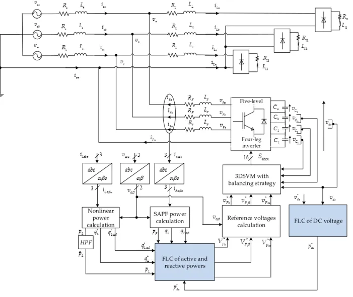
(II. 14): Five-level four-leg SAPF configuration ... 66
(II.15): DPC-3DSVM of five-level four-leg SAPF ... 68
(II.16): Regulation of DC voltage with a PI controller ... 72
(II.17): SAPF powers regulation by three PI controllers ... 73
(II.18): PDPC-3DSVM of five-level four-leg SAPF ... 75
(II.19): Predictive value estimation of reference powers ... 76
(II.20): Single-phase phasor diagram of the SAPF ... 77
(II.21): Current ripple during a switching period ... 79
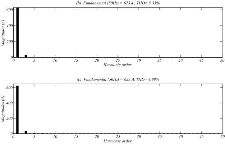
(II.22): (a): Source current before harmonics compensation, (b): Its harmonic spectrum ... 83
(II.23): (a): Source current after harmonics compensation using DPC-3DSVM, (b) Its harmonic spectrum ... 83
(II.24): (a): Source current after harmonics compensation using PDPC-3DSVM, (b) Its harmonic spectrum ... 84
(II.25): Simulation results of the five-level four-leg SAPF controlled by DPC-3DSVM under unbalanced load condition ... 86
(II.26): Simulation results of the five-level four-leg SAPF controlled by PDPC-3DSVM under unbalanced load condition ... 89
(II.27): Simulation results of the five-level four-leg SAPF controlled by DPC-3DSVM under distorted source voltage ... 92
(II.28): Simulation results of the five-level four-leg SAPF controlled by PDPC-3DSVM under distorted source voltage ... 94 (II.29): Harmonic spectrum of source current under distorted source voltage: (a)
compensation using PDPC-3DSVM ... 95
(II.30): Source current THD versus fifth harmonic voltage magnitude component (%) ... 95
(II.31): Source current THD versus, (a): coupling inductance variations ΔLF (%), (b): coupling resistance variations ΔRF (%) ... 96
(III.1): Block diagram of linearized MIMO system ... 100
(III.2): Dynamics of the linearized MIMO System ... 101
(III.3): Block diagram of closed loop of linearized MIMO system ... 102
(III.4): Feedback linearization of DPC-3DSVM for five-level four-leg SAPF ... 103
(III.5): Feedback linearization of PDPC-3DSVM for five-level four-leg SAPF ... 106
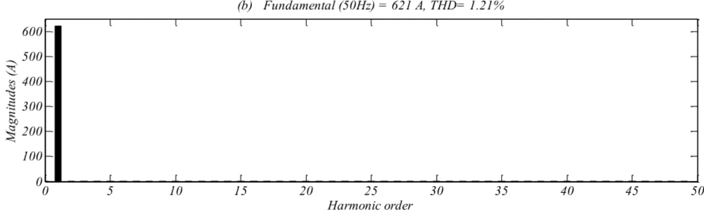
(III.6): (a): Source current before harmonics compensation, (b): Its harmonic spectrum ... 107
(III.7): (a): Source current after harmonics compensation using feedback linearization- DPC-3DSVM, (b) Its harmonic spectrum ... 108
(III.8): (a): Source current after harmonics compensation using Feedback linearization-PDPC-3DSVM, (b) Its harmonic spectrum ... 108
(III.9): Simulation results of the feedback linearization-DPC-3DSVM for the five-level four-leg SAPF under balanced and unbalanced load condition ... 110
(III.10): Simulation results of the feedback linearization-PDPC-3DSVM for the five- level four-leg SAPF under balanced and unbalanced load condition ... 112
(III.11): Simulation results of the five-level four-leg SAPF controlled by DPC under distorted source voltage ... 114
(III.12): Simulation results of the five-level four-leg SAPF controlled by DPC under distorted source voltage ... 116
(III.13): Harmonic spectrum of source current under distorted source voltage: (a) Before compensation, (b) After compensation using DPC-3DSVM, (c) After compensation using PDPC-3DSVM ... 117
(IV.1): Super-twisting controller trajectory in the phase plane ... 122
(IV.2): Super-twisting sliding mode control of DPC-3DSVM for five-level four-leg SAPF ... 124
(IV.3): Super-twisting sliding mode control of PDPC-3DSVM for five-level four-leg
SAPF ... 127
(IV.4): (a): Source current before harmonics compensation, (b): Its harmonic spectrum ... 128
(IV.5): (a): Source current after harmonics compensation using super-twisting-DPC- 3DSVM, (b) Its harmonic spectrum ... 129
(IV.6): (a): Source current after harmonics compensation using super-twisting -PDPC- 3DSVM, (b) Its harmonic spectrum ... 129
(IV.7): Simulation results of the Super-twisting-DPC-3DSVM for the five-level four- leg SAPF under balanced and unbalanced load condition ... 131
(IV.8): Simulation results of the Super-twisting-PDPC-3DSVM for the five-level four- leg SAPF under balanced and unbalanced load condition ... 133
(IV.9): Simulation results of the Super-twisting-DPC-3DSVM for the five-level four- leg SAPF under distorted source voltage ... 135
(IV.10): Simulation results of the Super-twisting-PDPC-3DSVM for the five-level four- leg SAPF under distorted source voltage ... 137
(IV.11): Harmonic spectrum of source current under distorted source voltage: (a) Before compensation, (b) After compensation using super-twisting-DPC- 3DSVM, (c) After compensation using super-twisting-PDPC-3DSVM ... 138
(V.1): Core, support and height of a fuzzy set ... 141
(V.2): Usual forms of membership functions ... 141
(V.3): Distribution of membership functions ... 142
(V.4): Block diagram of fuzzy logic controller ... 143
(V.5): Intern structure of the fuzzy logic controller proposed by Mamdani ... 145
(V.6): Distribution of chosen membership functions ... 146
(V.7): Fuzzy logic control of DPC-3DSVM for five-level four-leg SAPF ... 147
(V.8): Fuzzy logic control of PDPC-3DSVM for five-level four-leg SAPF ... 149
(V.9): (a): Source current before harmonics compensation, (b): Its harmonic spectrum ... 150 (V.10): (a): Source current after harmonics compensation using fuzzy logic -DPC-
3DSVM, (b) Its harmonic spectrum ... 151
(V.11): (a): Source current after harmonics compensation using fuzzy logic -PDPC-3DSVM, (b) Its harmonic spectrum ... 151
(V.12): Simulation results of the Fuzzy logic-DPC-3DSVM for the five-level four-leg SAPF during balanced and unbalanced load condition ... 153
(V.13): Simulation results of the Fuzzy logic-PDPC-3DSVM for the five-level four-leg SAPF during balanced and unbalanced load condition ... 155
(V.14): Simulation results of the fuzzy logic-DPC-3DSVM for the five-level four-leg SAPF under distorted source voltage ... 157
(V.15): Simulation results of the fuzzy logic-PDPC-3DSVM for the five-level four-leg SAPF under distorted source voltage ... 159
(V.16): Harmonic spectrum of source current under distorted source voltage, (a) Before compensation, (b) After compensation using fuzzy logic-DPC-3DSVM, (c) After compensation using fuzzy logic -PDPC-3DSVM ... 160
(V.17): Source current THD under balanced/unbalanced nonlinear load and distorted source voltage ... 161
(V.18): Neutral current ripple under unbalanced nonlinear load and distorted source voltage ... 161
(V.19): Source active and reactive powers ripples under balanced/unbalanced nonlinear load and distorted source voltage ... 161
(V.20): Source current THD versus coupling inductance variations ΔLF (%) ... 162
(V.21): Source current THD versus coupling resistance variations ΔRF (%) ... 163
List of tables
(I.1): Switching states of one leg of m-level four-leg inverter (x =a, b, c or n) ... 8
(I.2): Interchanging the switching states in all sectors ... 19
(I.3): Switching states of one leg of five-level four-leg inverter ... 28
(I.4): Prism identification in the first sector ... 32
(I.5): Number of tetrahedrons in each prism of the first sector ... 32
(I.6): Interchanging the switching states of each tetrahedron located in the same prism for the first sector ... 33
(II.1): Comparison of neutral current compensation methods in three-phase, four- wire system with different transformer configurations ... 59
(II.2): Comparison between three-phase four-wire SAPF topologies ... 65
(II.3): System parameters ... 82
(V.1): Fuzzy rules table ... 146
(V.2): Comparative study between all nonlinear techniques associated with DPC- 3DSVM and PDPC-3DSVM for five-level four-leg SAPF ... 165 (A.1): Localization condition of all tetrahedrons of the first sector
Symbols
Symbols Descriptions
xi
S Inverter switching states
xi
F Switching function
k
S Sector number
Angle of v* projected in αβ plane
angle of U* projected in αβ plane
M Modulation index i PR Prism number dc v DC-link voltage * dc
v DC-link voltage reference
j
C
v DC capacitor voltage of capacitance j
*
v Reference voltage vector
* * *
, and o
v v v Reference voltage vector components
*
U New reference voltage vector
* * *
, and o
U U U New reference voltage vector components
1, 2, 3 and 4
v v v v Adjacent switching vectors to the reference voltage vector
1, , and 2 3 4
t t t t On-duration time intervals of the switching vectors
, and
a b c
v v
v
Point of common coupling voltages,
and
Fa Fb Fc
v v
v
AC side voltages of the SAPF,
and
sa sb sc
v v
v
Source voltages, and o
v v v Voltages in αβo coordinates
k
i Inverter input currents
j
C
i Current through capacitor Cj
, , and
Fa Fb Fc Fn
i i i
i
AC side currents of the SAPF, , and La Lb Lc Ln i i i i Load currents , , and sa sb sc sn i i i i Source currents , and o
i i i Currents in αβo coordinates
dc
p Instantaneous DC power
,
L L
p q Active and reactive power of the nonlinear load
,
s s
p q Source active and reactive power
, and
L L Lo
*, *
F F
p q Active and reactive power references of SAPF
E Electrical energy stored in the chain of DC-link capacitors
min, max
E E Minimum and maximum energies stored in each capacitor
J Cost function C Capacitor eq C Equivalent capacitor Rs, Ls Source impedance RF, LF Filter impedance Rl, Ll Line impedance
Rl , Ll Diode rectifier load
fs Switching frequency f Fundamental frequency fe Sampling frequency Ts Switching period T fundamental period Te Sampling period
f (x) and h(x) Smooth vector fields
u and y Vectors ofinput and output
x State vector
Derivative number of an outputr Relative degree
,
f i g i
L h L h Lie derivatives of hi with respect to f and g
, p i k k PI coefficients ( ), ( ) and ( ) F F F p q q e k e k e k
Actual active and reactive power tracking errors
D(x) Decoupling matrix system
( )x
Linearization vector
v New input vector
Sliding surface
( )
Ax
s Degree of membershipA Fuzzy subset
Abbreviations
Abbreviations Descriptions
THD Total Harmonic Distorsion
IGBT Insolated Gate Bipolar Transistor GTO Gate Turn off Thyristor
PWM Pulse Width Modulation SVM Space Vector modulation
3DSVM Three-Dimensional Space Vector modulation
APF Active Power Filter
SAPF Shunt Active Power Filter
PCC Point of Common Coupling
PF Power Factor
VOC Voltage Oriented Control
DPC Direct Power Control
DPC-SVM Direct Power Control with Space Vector Modulation
DPC-3DSVM Direct Power Control with Three-Dimensional Space Vector modulation
PDPC Predictive Direct Power Control
PDPC-SVM Predictive Direct Power Control with Space Vector
Modulation
PDPC-3DSVM Predictive Direct Power Control with Three-Dimensional Space Vector Modulation
General introduction
In the recent years, the concept of smart distribution is taking shape. The emphasis of smart distribution system is on the efficiency enhancement by reducing distribution power losses, improving reliability, maximizing asset utilization, and better power quality free from harmonics [1]. Therefore, modern distribution systems are gaining significant attention over several power quality issues such as poor voltage regulation, high reactive power, harmonics current burden, phase unbalancing, excessive neutral line current, etc. [2]. In general, the source of these issues is secondary distribution system, which is directly connected to the customers. The secondary distribution is typically three-phase four-wire distribution system adopted to supply mixed loading, but it results in serious phase unbalance due to unequal distribution of single-phase loads [3]. Also, the presence of increasing number of non-linear loads such as adjustable speed drives, uninterruptible power supplies, etc. causes significant neutral current in the three-phase four-wire distribution system as tripled harmonics in phase currents [4]. Therefore, the total neutral line current is generated by the zero-sequence, fundamental, and harmonic components of the unbalanced load currents and thus results in the overload of neutral conductor of the three-phase four-wire distribution system [3]. The exponential growth in the nonlinear loads is responsible for further worsening of this situation. The study presented in [5] reveals that 22.6% of the distribution sites have a neutral line current in excess of 100%. The presence of phase unbalance and heavy neutral current are serious issues as they deteriorate the overall performance of distribution systems in many aspects, such as[4]:
- Increasing line losses,
- Deteriorating system voltage profiles, - Overloading system phases,
- Malfunctioning of protective relays,
- Saturating of distribution power transformers, - Increasing communication interference,
- Deteriorating power quality, system security and reliability of the electric supply, etc. There are various approaches reported in the literature for compensating neutral currents and harmonics problems in three-phase four-wire systems. Passive solutions such as
passive harmonic filters [6-8], synchronous machine [9], specially designed transformers [10-14] and active solutions such as three-phase four-wire active power filter (APF) [15-23]. Among power filtering solutions, shunt active power filters (SAPF) are specially designed for neutral current compensation and harmonic elimination in line-currents [18-19]. The commercial success of these filters is due to their acceptable cost, fast response time, flexibility of control and continuous operation with virtually no maintenance. Three main topologies are available for three-phase four-wire systems: three-phase four-wire capacitor midpoint (or split-capacitor) SAPF topology, three H-bridge SAPF topology, and three-phase four-leg SAPF topology [15-23].
In the first one, the neutral wire is connected to the midpoint of the DC-link capacitors. In [15-19], this approach was studied where the inverter was operating as an active power filter. However, although it is simple in terms of topology, this approach is not suitable for SAPF application, for the following reasons [18-19]: 1) insufficient DC-link utilization, 2) high ripple on DC-link capacitors, 3) problem of DC-link capacitor voltages balance. In the second topology, three single-phase H-bridge voltage source inverters are used to realize the four-wire SAPF. These H-bridge inverters are connected to the three-phase four-wire system by using three single-phase isolation transformers [18-20]. Since this topology requires a transformer, the four-wire SAPF size is large and the system energy efficiency is low. Slow response, increased number of switching devices, and high cost are the other disadvantages of this topology [18-19].
In the third topology the neutral wire is connected to the additional fourth leg [21-23]. This topology has been shown to be a solution for inverters operating in three-phase-four-wire systems and it offers full utilization of the DC-link voltage and lower stress on the DC-link capacitors [18-19].
Commonly, the abovementioned works are based on traditional two-level inverters. However, for medium to high power applications the multilevel inverters are the most attractive technology. Indeed, multilevel inverters have shown some significant advantages over traditional two-level inverters [24]-[27]. The main advantages of the multilevel inverters are a smaller output voltage step, lower harmonic components, a better electromagnetic compatibility and lower switching losses [24]-[27]. In the recent time, the use of multilevel inverters has been prevailing in medium-voltage active power filters without using a coupling transformer [28]-[32].
In other hand, the performance of the SAPF depends strongly on control strategies. In order to control the SAPF and achieve a proper power flow regulation in a power system, voltage-oriented control (VOC), which provides a good dynamic response by an internal current control loop, is widely used [33],[34]. As an alternative to this control method, other control strategies have been proposed in recent publications, such as predictive control and direct power control (DPC) [35]-[37].
DPC has become more widely used over the last few years due to the advantages of fast dynamic performance and simple control implementation when compared with other methods [35-37]. With DPC there are not internal current control loops and no PWM modulator bloc, because the inverter switching states are selected by a switching table based on the instantaneous errors between the commanded and estimated values of the
active / reactive powers, and voltage position vector. Therefore, the key point of the DPC implementation is the correct and fast estimation of the active and the reactive line powers. The DPC method is based on the direct torque control (DTC) which was originally proposed for controlling an induction motor in 1986 by Takahashi and Nogushi [38]. In 1995, Mannienen introduced basic principles of the DTC control method applied to the line inverter [39]. The structure of the line inverter may be exactly similar to the induction motor, the only exceptions being the connection to the grid instead of the induction motor and the introduction of the line filter. After that, the DPC was proposed by Noguchi in 1998 for PWM inverter without power source voltage sensors [40], and the same idea is developed by Malinowski in 2001 based on virtual flux estimation for three-phase PWM rectifiers system [41].
The main disadvantage of DPC with switching table is the variation of switching frequency, which generates an undesired broadband harmonic spectrum range and makes it hard to design a line filter [42]. These disadvantages can be effectively overcome by using space vector modulation (SVM) algorithm to replace the traditional switching table. The combination of SVM and traditional DPC forms the space vector modulation direct power control (SVM-DPC) [42].
Other structures of the DPC based on predictive approaches (Predictive Direct Power Control PDPC) have been recently published [43-47]. In view of switching frequency the PDPC methods can be divided into two groups: variable switching frequency and constant switching frequency. In the first group, the inverter’s switching states are selected based on the minimization of a cost function value, which defines the behavior of the system. However, in such approach, switching frequency is variable and its performance depends on sampling frequency, inverter load and parameters variations [43-46]. In the second group, a predictive control algorithm, using deadbeat control principle was developed to compute the required inverter average voltage vector [47]. The computed converter average voltage vector is generated during each switching period in order to cancel out simultaneously active and reactive power tracking errors. This voltage vector is used as input to SVM in order to generate the inverter’s switching states [47].
On other hand, the traditional two-dimensional SVM algorithm can be used only to control inverter connected to power system with balanced voltage/current where the hompolair component in Concordia transformation is equal to zero. In the three-phase four-wire system distribution, the case of unbalanced voltage/load is taken in consideration, therefore, the hompolair component is nonzero, and then, a three-dimensional space vector modulation (3DSVM) algorithm is needed in order to generate the desired signal.
In [48] and [49], 3DSVM schemes are analyzed for a four-leg two-level voltage source inverter. However, 3DSVM for a five-level four-leg inverter has not yet been studied in stationary reference frame. A novel algorithm of space vector modulation for a four-leg five-level inverter is proposed in this thesis.
The unbalance of the DC capacitor voltages is one of the most important drawbacks of the multilevel diode clamped inverter. Indeed, if any unbalance in the DC capacitor voltages appears, the output phase voltages/currents will be highly distorted which decreases the output signals quality [50-51].
Several approaches have been suggested to balance the DC capacitor voltages of diode clamped inverter [50-54]. In general, these schemes can be categorized into three major types. The first scheme [52] involves auxiliary balancing circuits, which incurs additional hardware costs. Second approach is applicable for the back-to-back converter topologies [53-54], where voltage balancing is achieved with the help of second converter; however it is impractical for the stand-alone diode clamped inverter applications [55]. The third approach for voltage balancing involves utilizing the redundancy in the switching patterns for the different control strategies [50-51]. This method has attained more focus these days, because no additional hardware cost is required and implementation becomes more feasible using high performance DSPs [50-51].
It is well established that conventional linear PI controllers are widely used in most industrial power electronics applications for the reasons of their simplicity and feasibility [56]. On the other hand, it is a fact that such kinds of controllers may fail to meet the high performance requirements of grid connected inverter applications due to their high vulnerability to the operation point, variations of the plant parameters and external disturbances.
Several control schemes based on linearization methods are proposed to achieve fast dynamic response to load and line disturbances [57-58]. Compared to PI controllers, they improve the general control performance of the SAPF [59-60].
Recently, fuzzy logic controllers [61-62] have received a great deal of attention in regards to their application to APFs. The advantages of fuzzy logic controllers over conventional controllers (PI) are that they do not require an accurate mathematical model, can work with imprecise inputs, can handle non-linearity, and are more robust than conventional PI controllers [61-62].
The sliding mode variable structure control (SMVSC) has been extensively studied so far owing to its robustness against parameter variations, external disturbances and model uncertainties. However; its main drawback is the chattering phenomenon, which restricts the SMVSC application [29].
With the intention of overcoming these disadvantages, Second Order Sliding Mode (SOSM) with Super-Twisting Control Law (STW) is proposed for the PWM rectifier in [64-65]. The STW is one of the most powerful second order continuous sliding mode control algorithms that handle a relative degree equal to one [65]. It generates a continuous control function that drives the sliding variable and its derivative to zero in finite time in the presence of the smooth matched disturbances with bounded gradient, when this boundary is known [64-65].
In this thesis, a three-phase five-level four-leg shunt active power filter is considered in the aim to improve power quality in four-wire systems. The use of the multilevel four-leg configuration can be justified by its ability to suppress the neutral current from the source without any drawback in the filtering performance and without using a coupling transformer. In the present work a simplified 3DSVM algorithm in αβo coordinates equipped by a balancing strategy is proposed to overcome the inherent instability of the DC capacitor voltages of four-leg multilevel inverter. Furthermore, in this thesis, new nonlinear control strategies based on the feedback linearization, super-twisting sliding mode, and fuzzy logic associated to DPC and PDPC using 3DSVM are proposed to control the five-level four-leg SAPF. The idea herein is to enhance the filtering system performance by controlling its active and reactive powers using an improved version of DPC and PDPC synthesized based on the aforementioned nonlinear control approaches. In order to achieve these research objectives, this thesis is divided into five chapters, which are summarized as follows:
The first chapter consists of two main parts. The first part is devoted to the modeling of m-level four-leg diode clamped inverter and a new simplified algorithm of 3DSVM is proposed. The second part deals with the problem of unbalance of the DC capacitor voltages at the input of the five-level four-leg inverter.
In the second chapter describes a comprehensive review of neutral current compensation methods, their topologies, and their technical and economical limitations are presented also. The objective of the second section of this chapter is to present a direct power control (DPC) and predictive direct power control (PDPC) with 3DSVM based on new model of five-level four-leg SAPF.
In the third and fourth chapters, nonlinear controllers based on the feedback linearization and second order sliding mode are associated to DPC and PDPC control in order to improve the performances of the five-level four-leg SAPF.
The fifth chapter is focused on the application of the fuzzy logic controller to regulate the DC voltage and active/reactive powers in both DPC-3DSVM and PDPC-3DSVM. Also, at the end of this chapter, a comparative study of the three previous nonlinear control techniques is presented.
Finally, a main conclusion of this dissertation and some recommendations for future research topics are provided.
Chapter
I
Modeling and control of four-leg
multilevel diode clamped inverter
I.1. Introduction
Multilevel inverters have opened the door for advances in electric energy conversion technology. They present the features of a lower device voltage rating, lower harmonic distortion, and higher efficiency compared with conventional two-level inverters [66-67]. These inverters are typically considered for high-power applications, because they allow operating at higher DC-link voltage levels with the currently available semiconductor technology [24, 70], [50-51]. However, they can also be interesting for medium- or even low-power/voltage applications, since they allow operating with lower voltage-rated devices, with potentially better performance/economical features [68-69].
There are three basic multilevel inverter topologies: diode clamped, flying capacitor, and cascaded H-bridge with separate DC sources. Among these topologies, diode-clamped inverters are especially interesting because of their simplicity; the multiple voltage levels are generated passively through a set of series-connected capacitors (see figure (I.1)). The simplest family member, the three-level inverter, has been widely studied [24], [69-70]. In four-wire systems, unbalanced or nonlinear loads and unbalanced sources can cause a large neutral current. The extra leg in four-leg inverters provides an effective neutral connection, which allows a precise control of the neutral current. The growing interest in four-leg inverters for three-phase four-wire systems focuses in applications such as distributed power inverters, active power filters, and fault-tolerant converters. Even with voltage-limited devices, the multilevel topologies can reach high power ratings with low
harmonic distortion, reduced switching losses and good electromagnetic compatibility [66-67]. However, the implementation of multilevel four-leg diode-clamped inverters, with four or more levels, still presents some challenges. By increasing the number of levels, the difficulty to ensure the voltage balance within the DC capacitors increases as well. This voltage imbalance can be caused by many factors such as operational conditions, load power factor, modulation index, as well as the modulation technique used [50-51].
The control of the four-leg inverter switches can be achieved by several modulation techniques [22, 48, 60], [71-75]. Among these modulation techniques, the space vector modulation (SVM) stands out because it offers significant flexibility to optimize switching waveforms, improvement in DC bus utilization, and it is well suited for digital implementation. Prior art of SVM for four-leg inverters is formulated in a three-dimension space (3DSVM) [22, 48, 60], [72-75]. Based on the effective use of the redundant switching states of the inverter voltage vectors, the 3DSVM can eliminate the problem of unbalancing DC-link capacitor voltages [60].
This chapter will consist of two main parts. The first part will be devoted to the modeling of m-level four-leg diode clamped inverter and a new simplified algorithm of 3DSVM will be proposed. The second section will deal with the problem of unbalance of the DC capacitor voltages at the input of the five-level four-leg inverter.
I.2. Ideal m-level four-leg diode-clamped inverter
Figure (I.1) shows a schematic diagram of a m-level four-leg diode-clamped inverter in which the DC-link consists of capacitors C1, C2, …, Cm-2 and Cm-1.
2 C 1 C 2 m C 1 m C 1 a S 2 a S ( 2) a m S (m1) S 1 a S 2 a S ( 2) a m S ( 1) a m S 0 1 2 3 m 2 m 1 m 1 dc v m 1 dc v m 1 dc v m 1 dc v m dc v
Corresponding to the net DC-link voltage of vdc, voltage across each capacitor is ideally
vdc/(m-1). Each leg consists of 2m-2 switches. There are m-1 complimentary switch pairs in
each leg. Using first leg as an example, the complementary pairs are
Sa1, Sa1
,
Sa2, Sa2
,...,
Sa m( 1), Sa m( 1)
. Gating signals Sa1, Sa2 ... Sa m( 1) are generated by inverting Sa1, Sa2 ... Sa m( 1) respectively.Considering voltage of node “0” as the reference voltage, the switching combinations to synthesize different voltage levels are summarized in table (I.1).
Table (I.1): Switching states of one leg of m-level four-leg inverter (x =a, b, c or n)
Switching states x1 S S …. x2 Sx m( 2) Sx m( 1) S x1 S …. x2 Sx m( 2) Sx m( 1) Output Phase voltage v x0 m-1 1 1 …. 1 1 0 0 …. 0 0 vdc m-2 0 1 …. 1 1 1 0 …. 0 0 ( 2) 1 dc m v m . . . . . . . . . . . . . . . . . . . . . . . . . . . . . . . . . . . . 1 0 0 …. 0 1 1 1 …. 1 0 dc1 v m 0 0 0 …. 0 0 1 1 …. 1 1 0
The switching functions are defined as Fij, where i
a b c n, , ,
is the phase index and
0,1, 1
j m is the voltage level. As shown in figure (I.2), the switching functions Fij
takes value “1” if i-phase is connected to voltage level j and “0” otherwise, these switching functions can be expressed as:
( 1) ( 1) ( 2) ( 3) 2 1 0 ( 2) ( 1) ( 2) ( 3) 2 1 0 ( 3) ( 1) ( 2) ( 3) 2 1 0 ... ... ... x m x m x m x m x x x x m x m x m x m x x x x m x m x m x m x x x F S S S S S S F S S S S S S F S S S S S S 2 ( 1) ( 2) ( 3) 2 1 0 1 ( 1) ( 2) ( 3) 2 1 0 0 ( 1) ( 2) ( 3) 2 1 0 , , or ... ... ... x x m x m x m x x x x x m x m x m x x x x x m x m x m x x x x a b c n F S S S S S S F S S S S S S F S S S S S S (I.1)
2 C 1 C 2 m C 1 m C 0 1 2 3 m 2 m 1 m 1 dc v m 1 dc v m 1 dc v m 1 dc v m dc v a v b v vc ( 1) a m F ( 2) a m F 0 a F ( 1) b m F ( 2) b m F 0 b F ( 1) c m F ( 2) c m F 0 c F ( 1) n m F 0 n F n v 1 m i 2 m i 3 m i 2 i 1 i 0 i
Figure (I.2): Schematic representation of the m-level four-leg inverter based on m-pole
Referring all of the voltages to the lower DC-link voltage level (“0” reference), each output voltage consists of contributions by a determinate number of consecutive capacitors:
1 0 0 0 , , , or i j m x xj C j i v F v x a b c n
(I.2)When balanced distribution of the DC-link voltage among the capacitors is assumed, the equation (I.2) becomes:
1 0 0 , , , or 1 m dc x xj j v v jF x a b c n m
(I.3) The instantaneous output inverter phase to neutral voltages va, vb and vc can be expressedas: 0 0 0 0 0 0 a a n b b n c c n v v v v v v v v v (I.4)
It can be expressed in terms of switching functions and DC-link voltages capacitors as given by: ( 1) ( 1) ( 2) ( 2) 1 1 0 0 ( 1) ( 1) ( 2) ( 2) 1 1 0 0 ( 1) ( 1) ( 2) ( 2) 1 1 0 0 ( 2) 1 1 0 dc dc a m n m a m n m a n a n a b b m n m b m n m b n b n c c m n m c m n m c n c n dc v m v F F F F F F F F v m v F F F F F F F F v F F F F F F F F v m (I.5)
The inverter input currents ik (k = 0, 1, ... , m-1) are expressed in terms of load currents ia, ib,
ic and in by:
k ak a bk b ck c nk n
i F i F i F i F i (I.6) In an m-level four-leg inverter, there are m4 possible switch combinations. The switch
combinations are represented by ordered sets
S S S Sa b c n
. Where: 1 2 1 0 x x x x S m S m S S ( 1) ( 2) 1 0 if 1 if 1 , , if 1 if 1 a m a m a a F F x a b c or n F F (I.7)The coordinates of each switching vector,v v, and vo are calculated by:
1 1 / 2 1 / 2 2 3 3 0 3 2 2 1 1 1 2 2 2 a b c o v v v v v v (I.8)
Using the different switching combinations, the vectors given by (I.8) can be described using a graphical representation in three-dimensional space as shown in figure (I.3).
There are (m-1) zero switching vectors, and
m4m unique non-zero switching vectors.
All the 4m switching vectors can be sorted into
m 1 6 1
layers.The diagram of space vectors can be divided into six sectors, each sector further is divided into
m 1
2 prisms and each prism is formed by tetrahedrons.Figure (I.3): Representation of space voltage vectors of m-level four-leg inverter in three-dimensional αβo plane
Projection of three-phase reference voltages into the o plane is a vector called the reference voltage vector *
v , it rotates counterclockwise in space diagram with angular frequency of as shown in figure (I.4).
o * v 1 6 1 m L a ye rs
3 2vdc * v 1 v 2 v 3 v 4 v o 2 2 1 3vdc m 1 2 1 3vdc m 3 2 1 3vdc m 3 level 2 level 4 level m level 2 2 1 3 dc m v m * v * v * v
I.2.1. Conventional three-dimensional space vector modulation
A 3DSVM is a discrete type of modulation technique in which a voltage reference vector *
v
is synthesized by the time average of a number of appropriate switching state vectors [48]. When the reference voltage vector is located in known sector and prism at any sampling instant, the tip of the voltage vector lies in a tetrahedron formed by the four switching vectors adjacent to it, (see figure (I.4)). The adjacent vectors necessary to synthesize the reference voltage vector related by:
* 1 1 2 2 3 3 4 4 1 2 2 4 s s v t v t v t v t v T t t t t T (I.9)
Where Ts is the switching period, v v1, , and 2 v3 v are the four switching vectors adjacent 4
to the reference voltage vector, and t1, , and t2 t3 t4 are their on-duration time intervals respectively.
The on-duration time intervals of appropriate switching vectors are calculated from the solution of (I.9).
Computational burden to synthesize a reference voltage is mostly associated with trigonometric calculations for: localization of the reference voltage vector, calculation of duration time intervals of adjacent switching vectors, and the generation of the corresponding pulses. This increases the required computational time and augments the hardware and software complexity [60].
I.3. Proposed algorithm of the three-dimensional space vector modulation
The proposed algorithm can reduce remarkably the complexity of 3DSVM by using one sector only in the conception of all modulation algorithm steps such as: determination of the space vector location, duration time calculation, and pulses generation [60].
The reference voltage vector rotates in the space αβo and crosses all the sectors (see figure (I.5)), then, it is necessary to build another vector *
U which turns only in the first sector and takes all information about *
v in the other sectors, as shown in figure (I.6). The components of the new reference voltage vector are:
* * * * * * cos( ) sin( ) o o U U U U U v (I.10) Where: U* v*2v*2 and mod( , ) 0, 3 3
mod(x,y): is a function which gives the division remainder of x on y.
and
are the angles of the vectors U* and v* projected in αβ plane respectively. The angle is given by:
* 1 * tan 2 v v (I.11)
And: tan2-1: is a function returns the four-quadrant inverse tangent.
Figure (I.5): Trajectory of reference voltage vector v*under unbalanced sinusoid condition, (a): Trajectory in three-dimensional space, (b): Projection of the trajectory on αβ plane
-1500 -1000 -500 0 500 1000 1500 -1000 -500 0 500 1000-500 0 500 v* (a) v* vo * -1500 -1000 -500 0 500 1000 1500 -1000 -500 0 500 1000 (b) v* v *
Figure (I.6):
Trajectory of reference voltage vector U*under unbalanced sinusoid condition, (a): Trajectory in
three-dimensional space, (b): Projection of the trajectory on αβ plane
I.3.1. Determination of the space vector location
The space vector location is determined in three steps: (1) determining the sector number of where the vector lies, (2) determining the number of prisms, and (3) determining the tetrahedron number of where the reference vector is located [60].
Step 1: Sector number computation
Sector numbers are given by:
300 400 500 600 700 800 900 1000 1100 1200 0 500 1000 -500 0 500 U* U* (a) U o * 3000 400 500 600 700 800 900 1000 1100 1200 100 200 300 400 500 600 700 800 900 U* U * (b)
ceil , 1,2,3,4,5,6 / 3 k S k (I.12) Where: ceil is the C-function that adjusts any real number to the nearest, but higher, integer.Step 2: Prisms identification
Reference vector U*is projected on the axes of 60° coordinate system as shown in figure (I.7) [30]. In the first sector, the normalized projected components are U1*and U*2 given by (I.13). * * * 1 * * 2 cos( ) sin( ) 3 2 3 1 2 sin( ) 3 2 3 1 dc dc U U U v m U U v m (I.13)
The modulation index is given by: * 2 3 dc U M v (I.14)
The equation (I.13) becomes:
* * * 1 * * 2 ( 1) cos( ) sin( ) 3 2 ( 1) sin( ) 3 U U M m U U M m U (I.15)
In order to identify the prism where the required reference voltage vector is located, the following integers are used:
* 1 1 * 2 2 int int l U l U (I.16) Where the int function returns the nearest integer that is less than or equal to its argument.The following criterion determines if the reference vector is located in a prism i (PRi) or
prism j (PRj) of the figure (I.7.a):
* * * 1 2 1 2 * * * 1 2 1 2 is in if: 1 is in if: 1 i j U PR U U l l U PR U U l l (I.17)
Step 3: Tetrahedron identification
The next step is to determine the tetrahedron number according to the location of the reference voltage. As shown in figure (I.7.b), each tetrahedron is limited from the top and the bottom by two planes.
1 U
* U 1 S * 1 U * 2 U 2 U (0, 0) (1, 0) (2, 0) (3, 0) (m 2, 0) (m 1, 0) (0,1) (0, 2) (0, 3) (0,m 2) (0,m 1) (1,m 2) (3, 3) (m 2,1) * U * U PRj i PRFigure (I.7): (a): Space voltage vectors for an m-level four-leg inverter in the first sector, (b): Example of a tetrahedron in a given prism
Each plane is created by three switching vectors. For example, the tetrahedron shown in figure (I.7.b), the top plane is formed by v1, v2 and v3, and bottom plane is formed by v2, v3
and v4. Equations of the top and bottom planes are written in the following form:
* * * 1 1 1 * * * 2 2 2 o o U a U b U c U a U b U c
(I.18)
Where: a1, a2, b1, b2, c1, c2 are constants, calculated by solving the equations (I.19) and (I.20):
1 1 1 1 2 2 1 2 1 3 3 3 1 1 1 o o o v v a v v v b v c v v v
(I.19) (a) (b) *
U
2v
3v
4v
1v
2 2 2 2 3 3 2 3 2 4 4 4 1 1 1 o o o v v a v v v b v c v v v
(I.20)
Where: vi,vi, and v iio, 1, 2, 3 or 4,are the components of the switching vector vi on αβo plane.
The localization condition of this tetrahedron is given by:
* * * 1 1 1 * * * 2 2 2 o o U a U b U c U a U b U c
(I.21)
I.3.2. Duration time calculation
In order to minimize the switching losses and to reduce the current ripple, switching vectors adjacent to the reference vector should be selected [48-51]. At any sampling instant, the tip of the voltage vector lies in a tetrahedron formed by the four switching vectors. The on-duration time intervals of each vector are obtained in accordance to the average value principle, which is given by [60]:
* 1 1 2 2 3 3 4 4 1 2 2 4 s s v t v t v t v t U T t t t t T (I.22) Expression (I.22) can by decomposed in the αβo coordinates system as follows:
* 1 2 3 4 1 * 1 2 3 4 2 * 3 1 2 3 4 4 1 1 1 1 s s o o o o o s s v v v v t U T v v v v t U T t v v v v U T t T
(I.23)
With the proposed algorithm, the on duration time intervals are calculated only in the first sector.
I.3.3. Pulse generation
The pulses are generated only in the first sector, the other sectors can deduced by simply interchanging the states of the output phases, each prism or switching vector in the first sector has an equivalence prism or switching vector in others sectors. This equivalence is detailed as follows:
- In odd sectors (3 and 5), we can find the equivalent vectors by rotating the first sector at an angle of 2π/3 for sector 3 and 4π/3 for sector 5.
- In pair sectors (2, 4 and 6), the equivalent vectors in the pair sectors can be determined by the projection of each vector of the first sector on the symmetry axis in pair sectors. The symmetry axis necessary to find the equivalence vectors in sector 2 is (Δ1) (see figure (I.8)). The symmetry axis (Δ2) is used for sector 4, and (Δ3)
for sector 6.
The states interchanging are given in table (I.2).
Table (I.2): Interchanging the switching states in all sectors
S1 S2 S3 S4 S5 S6 a b c n a b b a c c n n a b b c c a n n a a b c c b n n a c b a c b n n a c b b c a n n -level m 1 S 2 S 3 S 4 S 5 S 6 S 2-level 3-level 4-level 1 2 3 R eg ion 1 R eg ion 2 Region 2 Region 1 Reg ion 1 Reg ion 2 R eg ion 1 R eg io n 2 Region 1 Region 2 Reg ion 1 Reg ion 2
Figure (I.8): Switching vectors equivalences between the first sector and other sectors for an m-level four-leg inverter in αβ plane
Finely, the implementation procedure of the proposed 3DSVM algorithm is summarized in figure (I.9). * v Sector identification Sector= =1 New reference calculation Prism determination Tetrahedron identification Duration time calculation Pulses generation
States interchanging between sectors
Yes No First switching period Second switching period * U

![Figure (II.3) shows the basic system in which the synchronous machine is used for absorbing the zero-sequence harmonic currents [9, 19]](https://thumb-eu.123doks.com/thumbv2/123doknet/14479457.715517/74.892.135.816.616.938/figure-shows-synchronous-machine-absorbing-sequence-harmonic-currents.webp)
![Figure (II.11) shows the three H-bridge SAPF topology. It consists of three single-phase full bridge (H-bridge) inverters with a common self-supporting DC bus [18-20]](https://thumb-eu.123doks.com/thumbv2/123doknet/14479457.715517/81.892.171.773.807.1117/figure-bridge-topology-consists-single-bridge-inverters-supporting.webp)