HAL Id: hal-02946710
https://hal.archives-ouvertes.fr/hal-02946710
Submitted on 23 Sep 2020
HAL is a multi-disciplinary open access
archive for the deposit and dissemination of
sci-entific research documents, whether they are
pub-lished or not. The documents may come from
teaching and research institutions in France or
abroad, or from public or private research centers.
L’archive ouverte pluridisciplinaire HAL, est
destinée au dépôt et à la diffusion de documents
scientifiques de niveau recherche, publiés ou non,
émanant des établissements d’enseignement et de
recherche français ou étrangers, des laboratoires
publics ou privés.
Structural and electronic transitions in few layers of
isotopically pure hexagonal boron nitride
Jihene Zribi, Lama Khalil, José Avila, Julien Chaste, Hugo Henck, Fabrice
Oehler, Bernard Gil, Song Liu, James Edgar, Christine Giorgetti, et al.
To cite this version:
Jihene Zribi, Lama Khalil, José Avila, Julien Chaste, Hugo Henck, et al.. Structural and electronic
transitions in few layers of isotopically pure hexagonal boron nitride. Physical Review B, American
Physical Society, 2020, 102 (11), �10.1103/PhysRevB.102.115141�. �hal-02946710�
Electronic band structure and stacking orders in few-layers of
isotopically-pure hexagonal boron nitride
Jihene Zribi,
1Lama Khalil,
1José Avila,
2Julien Chaste,
1Hugo Henck,
1Fabrice Oehler,
1Bernard
Gil,
3Song Liu,
4James H. Edgar,
5Christine Giorgetti,
6Yannick J. Dappe,
7Emmanuel
Lhuillier,
8Guillaume Cassabois,
3Abdelkarim Ouerghi,
1*and Debora Pierucci
91
Université Paris-Saclay, CNRS, Centre de Nanosciences et de Nanotechnologies, 91120, Palaiseau,
France
2
Synchrotron SOLEIL and Université Paris-Saclay, L’Orme des Merisiers, BP48, 91190 Saint-Aubin,
France
3
Laboratoire Charles Coulomb (L2C), Université de Montpellier, CNRS, 34095 Montpellier, France
4Department of Mechanical Engineering, Columbia University, New York, NY 10027, USA
5Tim Taylor Department of Chemical Engineering, Kansas State University, Manhattan, Kansas 66506,
USA
6
Laboratoire des Solides Irradiés, CNRS, Ecole Polytechnique, CEA/DRF/IRAMIS, Institut
Polytechnique de Paris, F-91128 Palaiseau
7
SPEC, CEA, CNRS, Université Paris-Saclay, CEA Saclay, 91191 Gif-sur-Yvette Cedex, France
8Sorbonne Université, CNRS, Institut des NanoSciences de Paris, INSP, F-75005 Paris, France
9CELLS - ALBA Synchrotron Radiation Facility, Carrer de la Llum 2-26, 08290 Cerdanyola del Valles,
Barcelona, Spain
Hexagonal boron nitride (hBN) is attracting tremendous interest as an essential component in van der Waals heterostructures due to its ability to provide weakly interacting interfaces and because of its large bandgap. While exfoliated flakes of hBN have been widely investigated using ultraviolet optoelectronics, detailed experimental measurements of the electronic band structure are lacking. In fact, hBN has been predicted to exist in various crystallographic stacking sequences, which can strongly affect its optical and electronic properties. Here, we determine the electronic band structure and stacking order of few-layers of isotopically-pure exfoliated h11BN
flakes, using nanoscopic angle-resolved photoemission spectroscopy (nano-ARPES) combined with density functional theory (DFT) calculations. Additionally, the high crystalline quality and the thickness of the hBN flakes were determined by means of micro-Raman spectroscopy and atomic force microscopy (AFM), respectively. We demonstrate that hBN presents an AA’ stacking in its bulk form and an A’B stacking for 3 and 4 monolayers. Our findings open perspectives in understanding and controlling the stacking orders in hBN, which could be of great interest for applications.
INTRODUCTION
Layered two-dimensional (2D) materials are characterized by a strong anisotropy in the bonding energies along the crystal lattice directions. In-plane, the intra-layer bonding is mainly of the covalent type, while out-of-plane weak interlayer interactions dominate, usually with an overwhelming van-der-Waals (1) character. Most of the 2D compounds such as transition-metal dichalcogenides (2, 3) (TMDs) or hexagonal boron nitride (4) (hBN) can exist either in the bulk form or, as few- or mono-layer (ML). The ML form is often obtained from the bulk through simple mechanical exfoliation (5), envisaged upon breaking the weak inter-layer bonding.
Similarly to their 3D counterparts, 2D materials commonly present defects that may significantly affect their physical properties. The most common type of point defect in bulk and ML hBN is the natural isotope variation of boron (20 at% 10B and 80 at% 11B), which has provoked a particular interest in isotopically purified hBN (6–
9). Regardless the presence of isotopic disorder, some physical properties remain relatively unchanged: for
instance, natural hBN as well as pure h10BN and h11BN all possess a wide bandgap (10), low dielectric constant
(11), high mechanical strength (12, 13), and deep ultraviolet emission (14). However, compared to natural hBN, pure isotopic h10BN and h11BN show on one hand a much improved thermal conductivity (an increase of 40%),
and on the other hand a polariton lifetime an order of magnitude higher than natural hBN (6–8).
In addition to point defects, the weak out-of-plane bonding of 2D material facilitates the apparition of disorder in the crystal structure. Actually, various rotational and translational shifts may occur between the layers and affect the overall material properties (15–17). An example is the well-known Bernal stacking (ABA) in graphene that can transform into a rhombohedral (ABC) stacking with significant consequences on the electronic band structure9.
Structurally, hBN resembles graphite (18), with a 2D honeycomb structure relying on hexagonally organized sp2
-bonded boron and nitrogen atoms. However, as hBN possesses two types of atoms, other types of vertical stacking can occur. Among the five high-symmetry stacking configurations predicted for hBN (19–22), most of the synthesis techniques report the growth of the AA' (eclipsed) structure (23–27), where boron atoms in layer A lie directly below nitrogen atoms in layer A’. Recently, several experimental studies have demonstrated that few-layer hBN can adopt other stacking orders such as Bernal stacking (25, 28–31). In parallel to the experimental investigations, various theoretical studies using local-density approximation and generalized-gradient approximation calculations have anticipated that the AA’ and AB stacking are equally stable, both for the bulk and bilayer structures (32–34). Besides, van der Waals corrected density functional theory (DFT) approach claimed that bilayer hBN favors an AB’ stacking mode, where boron atoms are superimposed with boron atoms in the adjacent layer (35). These theoretical results are in stark contradiction with the experimental findings, where the AA’ form prevails overwhelmingly. Consequently, despite the large amount of literature devoted to this material, the origin of its various stacking sequences remains mostly unclear.
In this context, the direct visualization of the electronic band structure and its correlation with the stacking order of few layer hBN via angle-resolved photoemission spectroscopy (ARPES) is very interesting. Nevertheless, in absence of large scale samples, it is not possible to separate contributions from areas with different stacking sequence or/and number of layers. To overcome this issue, we use here nano-ARPES coupled with DFT calculations to restrict the analysis to nanometric sized (36),(37) regions with well-controlled thicknesses (of 3 ML, 4 ML and 10 ML) of mono-isotopic high quality h11BN crystals. Thanks to the experimental energy and
momentum resolution and to the calculated band structure, our results show that the stacking configuration is strongly correlated to the layer thickness and directly affects the electronic properties of the system. In particular, our findings reveal that surprisingly, hBN favors an AA’ stacking for 10 ML but an A’B stacking order is preferred when the number of layers are reduced to 3 or 4 ML.
RESULTS AND DISCUSSION
Figure 1 depicts a top view illustration of the five possible high-symmetry stacking sequences (AA, AB, AA’, AB’, A’B) and their band structure for trilayer hBN. All these sequences are limited to a two-layer motif, which repeats to form the polytype variation. In the case of odd number of layers, the structure is simply truncated to the appropriate number of layers (e.g., for 3ML AB, the polytype is ABA). For the sake of clarity, we only display a bilayer crystal structure, in which the atoms in the top layer are drawn smaller than the atoms in the bottom layer. The atoms of boron and nitrogen are represented in pink and blue colors, respectively. Although AA is the simplest stacking sequence (Fig. 1A), where atoms of the same type are superimposed (B on top of B and N on top of N), it constitutes a high-energy stacking configuration, and hence is energetically unstable. The experimentally observed stacking is AA’ (Fig. 1B), where B and N atoms alternate along the stacking axis (B on top of N and vice versa). Another stable structure, although less common, is the AB stacking (Fig. 1C), obtained from AA by translating every other layer by a single bond length. In this structure, half of the B atoms is superimposed with half of the N atoms, and the other half of atoms is located at the centers of the hexagons in the neighboring layers. By combining layer rotation and translation, we generate the AB’ and the A’B stacking faults (Figs. 1D-E). In the AB’ (A’B) configuration, the B (N) atoms are superimposed on the two layers, and the N (B) atoms are located at the center of the hexagons. In addition to the atomic structure, Figure 1 also shows the calculated electronic band structure for each polytype. As the latter strongly depends on the number of layers, we only consider a 3ML structure for all DFT calculations of Fig. 1. Although the overall dispersion looks nearly similar, there are differences between all polytypes, especially for the valence band near the K point (see also Fig. S1 for the electronic structure of bulk hBN). Particularly, comparing AA to A’B around the K point, we notice that the dispersion is almost identical, but the band splitting in energy is different. Besides, AA’, AB and AB’ all share the same band structure along the ΓK high symmetry direction, but disperse differently along ΓM. Therefore, our calculations clearly show that the stacking order directly affects the dispersion of the bands.
Figure 2 presents the sample employed in this study. It consists in an exfoliated monoisotopic h11BN crystal
transferred onto a graphene/SiC(0001) substrate. It should be pointed out that charging effects in photoemission from a bulk-like flake of an insulating material can be avoided by thinning the material in the exfoliation process and by placing it on a conductive support (38). Indeed, our recent photoemission study showed that it is possible to resolve the π-band of exfoliated hBN on epitaxial graphene (39). To quickly assess the crystalline and chemical
purity of our sample, we used micro-Raman (µ-Raman) spectroscopy. Figure 2A compares the µ-Raman spectrum obtained from our monoisotopic h11BN crystal with spectra from natural hNaBN and monoisotopic h10BN samples.
Only the high-energy active mode E2g is visible in the wavelength range between 1340 cm-1 and 1420 cm-1. This
mode corresponds to the stretching of the B-N bond within the hexagonal BN basal plane (40). The energy of this E2g phonon is 1356 cm-1, 1365 cm-1, and 1393 cm-1 for h11BN, hNaBN and h10BN, respectively. One should note
that the hNaBN peak is positioned between the peaks of h10BN and h11BN, since it is an isotopic mixture of both.
As obtained in previous studies (6, 8, 40–42), the Raman linewidths are significantly narrower for monoisotopic h10BN (3.8 ± 0.03 cm-1) and monoisotopich11BN (3.9 ± 0.02 cm-1) than for the naturally abundant hBN sample
(8.1 ± 0.1 cm-1). The small linewidth values for monoisotopic hBN crystals reflect the high crystalline quality of
these samples and indicate the absence of phonon scattering due to isotopic mass disorder (21).
Figures 2B-D show the region of interest, observed by optical microscopy, atomic force microscopy (AFM) and nano-ARPES. Optically, the transferred h11BN flake, marked with a white line, presents a slight contrast with
respect to the underlying graphene/SiC substrate, as shown in Fig. 2B. In the AFM image corresponding to Fig. 2B (see Fig. 2C), we can also identify the same flake (delimited by a white contour) on the stepped graphene/SiC surface. Notably, various thicknesses can be determined in the hBN region, assessed to be 3ML, 4 ML and 10 ML. It is worth noting that the lateral size of our exfoliated flake is much smaller than the conventional ARPES beam size (50 - 100 μm) (37), yet it is well within the range of nano-ARPES experiments, which can map the surface down to 100 nm lateral resolution. In Fig. 2D, we present the spatially resolved photoelectron intensity map for the same region on the sample, taken at a photon energy of 100 eV and integrated around the valence band maximum (VBM) along the ΓKM high symmetry direction. Based on our nano-ARPES measurements, we found that the h11BN Brillouin zone (BZ) was rotated by 39° with respect to the graphene BZ (Fig. S2). This arbitrary
twist angle simply stems from the transfer process of the h11BN flakes, which is performed without any rotational
control. The ARPES map in Fig. 2D clearly reveals the presence of various microscopic domains within the hBN flake. According to the AFM image, the area marked as 10 ML in the ARPES map where the intensity color scale is green, corresponds to the bulk region, while the other areas with lower intensity (blue color) are relative to 3 ML and 4 ML.
In Fig. 3A-C, we present the valence band structures along the ΓKM direction, obtained from three different points on the 10 ML, 4ML and 3ML regions of Fig. 2D, respectively. The sharpness of the different bands in all figures can be attributed to the high quality of the h11BN samples. At first sight, we remark that the π and σ bands signature
of the hBN band structure can be easily identified in all maps. On one hand, the π states disperse from the Γ point up towards the VBM located at the K point in the ΓK direction, then down to the M point in the KM direction. On the other hand, the σ bands, degenerate at the Γ point, disperse downwards to the K point. As established in our previous work on hBN flakes transferred onto a graphene underlayer (39), the quasiparticle bandgap of bulk hBN is of 6 eV, which indicates that our specimen in the B region exhibits a residual p-type doping character. Remarkably, we can notice from the spectra in Fig. 3 that the VBM downshifts from 2.94 eV binding energy (BE) for 10 ML to 3.1 eV BE for the 3 ML domain. This VBM shift of the π bands of about 0.16 eV when decreasing the thickness of hBN can be attributed to an interfacial electron transfer from the n-doped bilayer graphene to hBN. Actually, the charge transfer reduces the excess positive charge of hBN, similarly to what was reported for
the GaSe/graphene heterostructure (43). Since it only occurs at the interface, the reduction of the p doping is more pronounced for 3 ML and 4 ML than for bulk hBN. Note that the net dipole field between the graphene and hBN layers results from the short screening length along the c-axis.
In order to ascribe each electronic band structure of Figs. 3A-C to its corresponding crystallographic stacking sequence, we compared our experimental ARPES data with the band structure calculations in the DFT framework for free standing hBN layers (see Figs. 3D-F). The calculations also show the dispersion of the conduction band. Note that the DFT bands are shifted to account for the Fermi level position, and expanded by 17% in energy to match the experimental total bandwidth (44). This scaling effectively incorporates many-body interactions not included in the theory. The main features are well reproduced by the calculated band structures along all high symmetry directions for all ARPES spectra. For bulk hBN (Fig. 3D), a good agreement has been obtained between the measured band structure and DFT calculations according to the AA′ ordering. This proves that the most stable stacking order for bulk h11BN is AA′, consistent with previous experimental studies and theoretical predictions.
Moving to Figs. 3E and F, we remark that the nano-ARPES data are in accord with DFT calculations for the A’B stacking order. Therefore, the nano-ARPES maps clearly reveal that the band structure and the stacking order differ according to the layer thickness; this will be discussed more in detail in the coming paragraph.
Now, we mainly focus on the difference in the dispersion between the photoelectron intensity maps of Figs. 3D-F
around the K point (see Figs. 4A-C). We also included DFT calculations to our nano-ARPES data (see Figs. 4D-F) to make the comparison more effective. By comparing the dispersion of the π states in the nano-ARPES spectra of Fig. 4, we can notice that, specifically at the K point, the bands are degenerate for the 10 ML region, whereas they split into 3 and 4 parabolic branches for the 3 ML and 4 ML domains, respectively (see insets showing the second derivative). This difference in the electronic band structure, i.e., the π band degeneracy lifting for 3 ML and 4 ML with respect to 10 ML, mainly comes from a modification in the stacking order. Since the valence band structures of AA and A’B are quite similar, one could think of attributing the 3 ML and 4 ML electronic dispersion to the AA stacking configuration. However, the energy splitting between the π bands is higher for AA than for A’B, which eliminates the possibility of the energetically unstable AA stacking formation. Thus, we can deduce that hBN prefers an AA’ stacking for 10 ML and an A’B stacking for 3 ML and 4 ML, even though the well-known AA’ ordering is the most favorable one. Considering the spot size used in our nano-ARPES measurements, we argue that we are able to obtain large areas of 3 ML and 4 ML with an A’B structure. This indicates that BN is a promising candidate for the formation of large domains, presenting an exotic A’B stacking order.
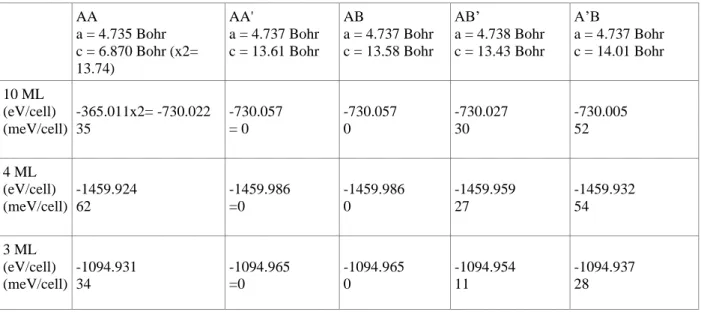
By means of DFT, we also calculated the total cohesive energies for 3 ML, 4 ML and for the bulk crystal in the five possible different stacking orders presented in Fig. 1. Quantitatively, the computed energy values are summarized in Table 1. As above-mentioned, the AA’ stacking, where the hexagons are superposed with an alternation of B and N atoms in each column, is considered to be the natural stacking of hBN. Our results show that it is indeed the phase which presents the lowest total energy for the bulk, as well as for 3ML and 4 ML. Therefore, we took it as the reference, and set its energy to zero. In the AB phase, the atoms can be either in the middle of the hexagons, and thus without neighbors in the adjacent layers, or piled up in columns with an alternation of B and N atoms. The fact that some columns are “missing” has consequences on the relaxed geometry,
which presents a smaller c length with respect to AA’. However, due to the alternate piling in the remaining columns, the configuration is equally stable to AA’, regardless the number of layers. When the columns are only made of N atoms (the case of A’B), the c length presents the highest numerical value (14.01 Bohr), whereas when they consist only of B atoms (the AB’ case), the c length becomes the smallest (13.43 Bohr). For the AA stacking, where both kinds of columns made of either N or B atoms are present, the cell length c has a value in-between the ones of A’B and AB’ (13.74 Bohr)
.
Concerning the total energy, the latter three phases (namely, A’B, AB’ and AA) are less stables than the AA’ and AB ones. Among these three stackings, the AB’ is the most stable one. The comparison of its electronic band structure with the experimental one, and in particular the fact the three top valence bands at Γ are degenerate, allows us to exclude that we are measuring this stacking.
Thus, the two remaining geometries in which the degeneracy is lifted are AA and A’B. In particular, for the AA structure, one can clearly notice from Table 1 that it is the most stable bulk configuration compared to A’B. However, this is not the case for the 3 and 4-layer geometries. This confirms, in addition to the values of the shift of the VBM, that we obtained an A’B stacking for few layer hBN. To further confirm the obtention of this stacking, one should measure the unoccupied electronic band structure by means of inverse photoemission or by time-resolved ARPES. Finally, we found from our calculations that the stacking orders can be strongly affected by the interlayer distance between hBN and graphene. Therefore, it is the key parameter that induces the modification in the stacking order of hBN.In summary, we have successfully conducted high-resolution nano-ARPES experiments on high-quality exfoliated monoisotopic h11BN crystals. Our experimental results coupled with theoretical calculations show that the stacking
order for multilayer (few-layer) h11BN is AA′ (A’B). The dispersion of the π bands is changed according to the
stacking sequence, specifically at the K point. In particular, for bulk hBN, the π bands are degenerate at the K point, whereas for few-layer hBN, the degeneracy is lifted and these states reveal a splitting in energy. By taking into account the spot size of the nano-ARPES beam, we argue that we have obtained large domains presenting an exotic A’B stacking order for 3ML and 4 ML. In perspective, further theoretical investigations are required to understand the interplay between the stacking order and the layer thickness after mechanical exfoliation of hBN samples.
METHODS
Mechanical exfoliation and transfer
Mechanical exfoliation of the transferred monoisotopic h11BN flakes on the graphene substrate was carried out
using the standard scotch tape technique.
µ-Raman and AFM measurements
The µ-Raman measurements were conducted at room temperature, using a commercial confocal Renishaw micro-Raman microscope with a 100× objective and a 532 nm laser excitation. The laser beam was focused onto a small spot having a diameter of ~1 μm on the sample and its incident power was about 5 mW. The AFM measurements were performed on a Veeco AFM.
nano-ARPES measurements
The nano-ARPES experiments were performed at the ANTARES beamline of the SOLEIL synchrotron light source (Saint-Aubin, France). The nano-ARPES data were taken at a photon energy of 100 eV, using linearly
polarized light. All measurements were carried out at a base pressure of 5 × 10⁻¹¹ mbar and a base temperature of 70 K.
DFT calculations
Cell optimization, total energy and band structure have been calculated within the ab initio framework of density functional theory using the Abinit code (45). We used the Perdrew-Burke-Ernzerhof generalized gradient approximation for the exchange and correlation energy (46) and optimized norm-conserving Vanderbild pseudopotential (47). Each boron atom participates with 3 valence electrons (2s2 2p1) and each nitrogen atom with 5 (2s2 2p3). The van der Waals interactions have been accounted within the vdW-DFT-D3 scheme proposed by S. Grimme (48).
The full optimization of the unit cell was done on the bulk counterpart of each compound. The values of the in-plane (a) and perpendicular to the in-plane (c) lengths of the unit cell after optimization are summarized in the first line of table (45). Using these cell parameters, a stacking of 3 layers and 4 layers of each compound have been built and introduced into a large supercell to mimic an isolated slab. The density has been computed Monkhorst-Pack grid of (11 x 11 x 2) k-points, with an energy cutoff of 32 Hartree. The band structures have been sampled with 41 points along GK and GM. The total energies are reported in table 1 for the bulk, the 3 layers and 4 layers for the five stacking. Energies are referenced to the AA' stacking, and are in meV per unit cell (two B and two N atoms).
SUPPLEMENTARY MATERIALS
Supplementary material for this article is available at….
Fig. S1. Electronic band structure calculations of bulk h11BN for the five possible high-energy stacking
configurations.
Fig. S2. Angle between graphene and hBN.
Fig. S3. Reference spectra for µ-Raman spectroscopy and AFM measurements.
FIGURE CAPTIONS
Fig. 1: Top view representation of the five possible high-symmetry stacking orders of hBN together with their 3ML calculated electronic band structure. Different sequences are obtained by interlayer translation (AB),
rotation (AA′) or both (AB′ and A’B) from the AA stacking order, where atoms of the same type are superimposed (B on B and N on N).
Fig. 2: Structural and electronic properties of the exfoliated h11BN crystal. (A) µ-Raman spectra acquired at
room temperature from three different hBN samples, namely, the monoisotopic h10BN and h11BN crystals and the
standard hNaBN specimen. (B) Typical optical image, in which the h11BN domains exhibit a slight different contrast
with respect to the graphene substrate. (C) AFM image of the region delimited by a white contour in Fig. 2B. (D) A spatially resolved intensity map, integrated around the VBM along the ΓKM high symmetry direction, around the region delimited by a white dashed line in the optical image of Fig. 2B.
Fig. 3: nano-ARPES study. Comparison of the experimental electronic band structure (acquired with a 100 eV
of photon energy) between (A) 10 ML, (B) 4 ML and (C) 3 ML of hBN. DFT calculations were also included to the photoelectron intensity maps in Figs. 3D-F for 10 ML, 4 ML and 3 ML of hBN, respectively.
Fig. 4: nano-ARPES study around the K point. Comparison of the dispersion around the K point of the ARPES
spectra of Figs. D-F between (A) 10 ML, (B) 4 ML, and (C) 3 ML of hBN. DFT calculations were also included to the nano-ARPES yields in Figs. 4D-F for 10 ML, 4 ML and 3 ML of hBN, respectively. Insets display the second derivatives of the photoelectron intensity maps of Figs. 4E and F. Blue arrows indicate the presence of 3 and 4 parabolic branches for 3 ML and 4 ML, respectively.
Table 1: Computed total energies of the five high-symmetry stacking configurations of 10 ML, 4 ML and 3 ML
hBN. AA a = 4.735 Bohr c = 6.870 Bohr (x2= 13.74) AA' a = 4.737 Bohr c = 13.61 Bohr AB a = 4.737 Bohr c = 13.58 Bohr AB’ a = 4.738 Bohr c = 13.43 Bohr A’B a = 4.737 Bohr c = 14.01 Bohr 10 ML (eV/cell) (meV/cell) -365.011x2= -730.022 35 -730.057 = 0 -730.057 0 -730.027 30 -730.005 52 4 ML (eV/cell) (meV/cell) -1459.924 62 -1459.986 =0 -1459.986 0 -1459.959 27 -1459.932 54 3 ML (eV/cell) (meV/cell) -1094.931 34 -1094.965 =0 -1094.965 0 -1094.954 11 -1094.937 28 REFERENCES
1. K. S. Novoselov, A. Mishchenko, A. Carvalho, A. H. C. Neto, O. Road, 2D materials and van der Waals heterostructures. Science (80-. ). 353, aac9439 (2016).
2. R. Cheng, S. Jiang, Y. Chen, Y. Liu, N. Weiss, H.-C. Cheng, H. Wu, Y. Huang, X. Duan, Few-layer molybdenum disulfide transistors and circuits for high-speed flexible electronics. Nat. Commun. 5, 5143 (2014).
3. R. Cheng, D. Li, H. Zhou, C. Wang, A. Yin, S. Jiang, Y. Liu, Y. Chen, Y. Huang, X. Duan,
Electroluminescence and Photocurrent Generation from Atomically Sharp WSe2/MoS2 Heterojunction p-n Diodes. Nano Lett. 14, 5590–5597 (2014).
4. G. Cassabois, P. Valvin, B. Gil, Hexagonal boron nitride is an indirect bandgap semiconductor. Nat.
Photonics. 10, 262–266 (2016).
5. K. S. Novoselov, A. K. Geim, S. V. Morozov, D. Jiang, Y. Zhang, Dubonos S. V., Grigorieva I. V., A. A. Firsov, Electric Field Effect in Atomically Thin Carbon Films. Science (80-. ). 306, 666–669 (2004). 6. A. J. Giles, S. Dai, I. Vurgaftman, T. Hoffman, S. Liu, L. Lindsay, C. T. Ellis, N. Assefa, I. Chatzakis, T.
L. Reinecke, J. G. Tischler, M. M. Fogler, J. H. Edgar, D. N. Basov, J. D. Caldwell, Ultralow-loss polaritons in isotopically pure boron nitride. Nat. Mater. 17, 134–139 (2018).
7. T. Q. P. Vuong, S. Liu, A. Van Der Lee, R. Cuscó, L. Artús, T. Michel, P. Valvin, J. H. Edgar, G. Cassabois, B. Gil, Isotope engineering of van derWaals interactions in hexagonal boron nitride. Nat.
Mater. 17, 152–158 (2018).
8. C. Yuan, J. Li, L. Lindsay, D. Cherns, J. W. Pomeroy, S. Liu, J. H. Edgar, M. Kuball, Modulating the thermal conductivity in hexagonal boron nitride via controlled boron isotope concentration. Commun.
Phys. 2, 43 (2019).
9. R. Cuscó, L. Artús, J. H. Edgar, S. Liu, G. Cassabois, B. Gil, Isotopic effects on phonon anharmonicity in layered van der Waals crystals: Isotopically pure hexagonal boron nitride. Phys. Rev. B. 97 (2018), doi:10.1103/PhysRevB.97.155435.
10. Y. Kubota, K. Watanabe, O. Tsuda, T. Taniguchi, Deep Ultraviolet Light–Emitting Hexagonal Boron Nitride Synthesized at Atmospheric Pressure. Science (80-. ). 317, 932–934 (2007).
11. H. Yang, H. Fang, H. Yu, Y. Chen, L. Wang, W. Jiang, Y. Wu, J. Li, Low temperature self-densification of high strength bulk hexagonal boron nitride. Nat. Commun. 10, 854 (2019).
12. C. Zhi, Y. Bando, C. Tang, H. Kuwahara, D. Golberg, Large-scale Fabrication of Boron Nitride Nanosheets and Their Utilization in Polymeric Composites with Improved Thermal and Mechanical Properties. Adv. Mater. 21, 2889–2893 (2009).
13. K. K. Kim, A. Hsu, X. Jia, S. M. Kim, Y. Shi, M. Hofmann, D. Nezich, J. F. Rodriguez-Nieva, M. Dresselhaus, T. Palacios, J. Kong, Synthesis of Monolayer Hexagonal Boron Nitride on Cu Foil Using Chemical Vapor Deposition. Nano Lett. 12, 161–166 (2012).
14. T. Q. P. Vuong, G. Cassabois, P. Valvin, E. Rousseau, A. Summerfield, C. J. Mellor, Y. Cho, T. S. Cheng, J. D. Albar, L. Eaves, C. T. Foxon, P. H. Beton, S. V. Novikov, B. Gil, Deep ultraviolet emission in hexagonal boron nitride grown by high-temperature molecular beam epitaxy. 2D Mater. 4, 021023 (2017).
15. R. Ribeiro-Palau, C. Zhang, K. Watanabe, T. Taniguchi, J. Hone, C. R. Dean, Twistable electronics with dynamically rotatable heterostructures. Science (80-. ). 361, 690–693 (2018).
16. C.-J. Kim, L. Brown, M. W. Graham, R. Hovden, R. W. Havener, P. L. McEuen, D. A. Muller, J. Park, Stacking Order Dependent Second Harmonic Generation and Topological Defects in h-BN Bilayers.
Nano Lett. 13, 5660–5665 (2013).
17. Y. Cao, V. Fatemi, S. Fang, K. Watanabe, T. Taniguchi, E. Kaxiras, P. Jarillo-Herrero, Unconventional superconductivity in magic-angle graphene superlattices. Nature. 556, 43–50 (2018).
18. D. Pacilé, J. C. Meyer, Ç. Ö. Girit, A. Zettl, The two-dimensional phase of boron nitride: Few-atomic-layer sheets and suspended membranes. Appl. Phys. Lett. 92, 133107 (2008).
19. S. M. Gilbert, T. Pham, M. Dogan, S. Oh, B. Shevitski, G. Schumm, S. Liu, P. Ercius, S. Aloni, M. L. Cohen, A. Zettl, Alternative stacking sequences in hexagonal boron nitride. 2D Mater. 6, 021006 (2019). 20. G. Constantinescu, A. Kuc, T. Heine, Stacking in Bulk and Bilayer Hexagonal Boron Nitride. Phys. Rev.
Lett. 111, 036104 (2013).
21. H. Henck, D. Pierucci, Z. Ben Aziza, M. G. Silly, B. Gil, F. Sirotti, G. Cassabois, A. Ouerghi, Stacking fault and defects in single domain multilayered hexagonal boron nitride. Appl. Phys. Lett. 110, 023101 (2017).
22. R. M. Ribeiro, N. M. R. Peres, Stability of boron nitride bilayers: Ground-state energies, interlayer distances, and tight-binding description. Phys. Rev. B. 83, 235312 (2011).
23. R. S. Pease, Crystal Structure of Boron Nitride. Nature. 165, 722–723 (1950).
24. S. M. Kim, A. Hsu, M. H. Park, S. H. Chae, S. J. Yun, J. S. Lee, D.-H. Cho, W. Fang, C. Lee, T. Palacios, M. Dresselhaus, K. K. Kim, Y. H. Lee, J. Kong, Synthesis of large-area multilayer hexagonal boron nitride for high material performance. Nat. Commun. 6, 8662 (2015).
25. J. H. Warner, M. H. Rümmeli, A. Bachmatiuk, B. Büchner, Atomic Resolution Imaging and Topography of Boron Nitride Sheets Produced by Chemical Exfoliation. ACS Nano. 4, 1299–1304 (2010).
26. N. Alem, R. Erni, C. Kisielowski, M. D. Rossell, W. Gannett, A. Zettl, Atomically thin hexagonal boron nitride probed by ultrahigh-resolution transmission electron microscopy. Phys. Rev. B. 80, 155425 (2009).
27. W. J. Yu, W. M. Lau, S. P. Chan, Z. F. Liu, Q. Q. Zheng, Ab initio study of phase transformations in boron nitride. Phys. Rev. B. 67, 014108 (2003).
Nellist, V. Nicolosi, Impurity induced non-bulk stacking in chemically exfoliated h-BN nanosheets.
Nanoscale. 5, 2290–2294 (2013).
29. C.-J. Kim, L. Brown, M. W. Graham, R. Hovden, R. W. Havener, P. L. McEuen, D. A. Muller, J. Park, Stacking Order Dependent Second Harmonic Generation and Topological Defects in h-BN Bilayers.
Nano Lett. 13, 5660–5665 (2013).
30. M. H. Khan, G. Casillas, D. R. G. Mitchell, H. K. Liu, L. Jiang, Z. Huang, Carbon- and crack-free growth of hexagonal boron nitride nanosheets and their uncommon stacking order. Nanoscale. 8, 15926– 15933 (2016).
31. M. H. Khan, H. K. Liu, X. Sun, Y. Yamauchi, Y. Bando, D. Golberg, Z. Huang, Few-atomic-layered hexagonal boron nitride: CVD growth, characterization, and applications. Mater. Today. 20, 611–628 (2017).
32. J. L. Yin, M. L. Hu, Z. Yu, C. X. Zhang, L. Z. Sun, J. X. Zhong, Direct or indirect semiconductor: The role of stacking fault in h-BN. Phys. B Condens. Matter. 406, 2293–2297 (2011).
33. N. Ooi, A. Rairkar, L. Lindsley, J. B. Adams, Electronic structure and bonding in hexagonal boron nitride. J. Phys. Condens. Matter. 18, 97–115 (2006).
34. L. Liu, Y. P. Feng, Z. X. Shen, Structural and electronic properties of h-BN. Phys. Rev. B. 68, 104102 (2003).
35. N. Marom, J. Bernstein, J. Garel, A. Tkatchenko, E. Joselevich, L. Kronik, O. Hod, Stacking and Registry Effects in Layered Materials: The Case of Hexagonal Boron Nitride. Phys. Rev. Lett. 105, 046801 (2010).
36. D. Pierucci, H. Henck, J. Avila, A. Balan, C. H. Naylor, G. Patriarche, Y. J. Dappe, M. G. Silly, F. Sirotti, A. T. C. Johnson, M. C. Asensio, A. Ouerghi, Band Alignment and Minigaps in Monolayer MoS2-graphene van der Waals Heterostructures. Nano Lett. 16, 4054–4061 (2016).
37. H. Henck, J. Avila, Z. Ben Aziza, D. Pierucci, J. Baima, B. Pamuk, J. Chaste, D. Utt, M. Bartos, K. Nogajewski, B. A. Piot, M. Orlita, M. Potemski, M. Calandra, M. C. Asensio, F. Mauri, C. Faugeras, A. Ouerghi, Flat electronic bands in long sequences of rhombohedral-stacked graphene. Phys. Rev. B. 97, 245421 (2018).
38. R. J. Koch, J. Katoch, S. Moser, D. Schwarz, R. K. Kawakami, A. Bostwick, E. Rotenberg, C. Jozwiak, S. Ulstrup, Electronic structure of exfoliated and epitaxial hexagonal boron nitride. Phys. Rev. Mater. 2, 074006 (2018).
39. H. Henck, D. Pierucci, G. Fugallo, J. Avila, G. Cassabois, Y. J. Dappe, M. G. Silly, C. Chen, B. Gil, M. Gatti, F. Sottile, F. Sirotti, M. C. Asensio, A. Ouerghi, Direct observation of the band structure in bulk hexagonal boron nitride. Phys. Rev. B. 95, 085410 (2017).
40. T. Q. P. Vuong, S. Liu, A. Lee Van der, R. Cuscó, L. Artús, T. Michel, P. Valvin, J. H. Edgar, G. Cassabois, B. Gil, Isotope engineering of van der Waals interactions in hexagonal boron nitride. Nat.
Mater. 17, 152–158 (2018).
41. S. Liu, R. He, L. Xue, J. Li, B. Liu, J. H. Edgar, Single Crystal Growth of Millimeter-Sized Monoisotopic Hexagonal Boron Nitride. Chem. Mater. 30, 6222–6225 (2018).
42. A. J. Giles, S. Dai, I. Vurgaftman, T. Hoffman, S. Liu, L. Lindsay, C. T. Ellis, N. Assefa, I. Chatzakis, T. L. Reinecke, J. G. Tischler, M. M. Fogler, J. H. Edgar, D. N. Basov, J. D. Caldwell, Ultralow-loss polaritons in isotopically pure boron nitride. Nat. Mater. 17, 134–139 (2018).
43. Z. Ben Aziza, D. Pierucci, H. Henck, M. G. Silly, C. David, M. Yoon, F. Sirotti, K. Xiao, M. Eddrief, J.-C. Girard, A. Ouerghi, Tunable quasiparticle band gap in few-layer GaSe/graphene van der Waals heterostructures. Phys. Rev. B. 96, 035407 (2017).
44. D. Pierucci, H. Sediri, M. Hajlaoui, J. Girard, T. Brumme, M. Calandra, E. Velez-fort, G. Patriarche, M. G. Silly, G. Ferro, G. Yvette, I. De Minéralogie, D. P. Matériaux, D. Cosmochimie, U. M. R. Cnrs, S. Universités, Evidence for Flat Bands near the Fermi Level in Epitaxial Rhombohedral Multilayer Graphene. ACS Nano, 5432–5439 (2015).
45. X. Gonze, B. Amadon, P.-M. Anglade, J.-M. Beuken, F. Bottin, P. Boulanger, F. Bruneval, D. Caliste, R. Caracas, M. Côté, T. Deutsch, L. Genovese, P. Ghosez, M. Giantomassi, S. Goedecker, D. R. Hamann, P. Hermet, F. Jollet, G. Jomard, S. Leroux, M. Mancini, S. Mazevet, M. J. T. Oliveira, G. Onida, Y. Pouillon, T. Rangel, G.-M. Rignanese, D. Sangalli, R. Shaltaf, M. Torrent, M. J. Verstraete, G. Zerah, J. W. Zwanziger, ABINIT: First-principles approach to material and nanosystem properties.
Comput. Phys. Commun. 180, 2582–2615 (2009).
46. J. P. Perdew, K. Burke, M. Ernzerhof, Generalized Gradient Approximation Made Simple. Phys. Rev.
Lett. 77, 3865–3868 (1996).
47. D. R. Hamann, Optimized norm-conserving Vanderbilt pseudopotentials. Phys. Rev. B. 88, 085117 (2013).
48. S. Grimme, J. Antony, S. Ehrlich, H. Krieg, A consistent and accurate ab initio parametrization of density functional dispersion correction (DFT-D) for the 94 elements H-Pu. J. Chem. Phys. 132, 154104 (2010).
ACKNOWLEDGMENTS
Funding: We acknowledge the financial support by RhomboG (ANR-17-CE24-0030) and MagicValley grants.
This work is supported by a public grant overseen by the French National Research Agency (ANR) as part of the “Investissements d’Avenir” program (Labex NanoSaclay, reference: ANR-10-LABX-0035). Author
Contributions: ... Competing interests: The authors declare no competing financial interests. Data availability:
The datasets generated during or/and analyzed during the current study are available from the corresponding author on reasonable request.