Publisher’s version / Version de l'éditeur:
Vous avez des questions? Nous pouvons vous aider. Pour communiquer directement avec un auteur, consultez la première page de la revue dans laquelle son article a été publié afin de trouver ses coordonnées. Si vous n’arrivez pas à les repérer, communiquez avec nous à [email protected].
Questions? Contact the NRC Publications Archive team at
[email protected]. If you wish to email the authors directly, please see the first page of the publication for their contact information.
https://publications-cnrc.canada.ca/fra/droits
L’accès à ce site Web et l’utilisation de son contenu sont assujettis aux conditions présentées dans le site LISEZ CES CONDITIONS ATTENTIVEMENT AVANT D’UTILISER CE SITE WEB.
Nano Letters, 5, 5, pp. 815-819, 2005-01-29
READ THESE TERMS AND CONDITIONS CAREFULLY BEFORE USING THIS WEBSITE. https://nrc-publications.canada.ca/eng/copyright
NRC Publications Archive Record / Notice des Archives des publications du CNRC :
https://nrc-publications.canada.ca/eng/view/object/?id=1cc80b10-97b6-4161-9654-2daf7d7c7e6d
https://publications-cnrc.canada.ca/fra/voir/objet/?id=1cc80b10-97b6-4161-9654-2daf7d7c7e6d
NRC Publications Archive
Archives des publications du CNRC
This publication could be one of several versions: author’s original, accepted manuscript or the publisher’s version. / La version de cette publication peut être l’une des suivantes : la version prépublication de l’auteur, la version acceptée du manuscrit ou la version de l’éditeur.
For the publisher’s version, please access the DOI link below./ Pour consulter la version de l’éditeur, utilisez le lien DOI ci-dessous.
https://doi.org/10.1021/nl048008k
Access and use of this website and the material on it are subject to the Terms and Conditions set forth at
Silver nano-inukshuks on germanium
Silver Nano-Inukshuks on Germanium
Masato Aizawa,
†,§Anne M. Cooper,
§Marek Malac,
‡,§and Jillian M. Buriak*
,†,§Department of Chemistry, Department of Physics, and National Institute for Nanotechnology, UniVersity of Alberta, Edmonton, AB T6G 2G2
Received December 1, 2004
ABSTRACT
The integration of metallic nanostructures with semiconductors is important for a variety of technological applications. Through an efficient galvanic displacement reaction on germanium, complex silver nanostructures form spontaneously in aqueous conditions at room temperature. The structures, termed nano-inukshuks, are based on stacks of hexagonal metallic structures that grow, initially, parallel to the surface normal of the germanium. TEM, SEM, XPS, XRD, and EDS indicate that the structures are crystalline silver and, based on open cell potential studies, that their nucleation takes place in the first 100 s, followed by growth of the silver structures, most likely through Volmer−Weber growth.
In the Arctic, the Inuit peoples build stark, beautiful structures called inukshuks out of flat slabs of rock to mark trails and other important places on the flat landscape of the North; one example of these diverse structural forms is shown in Figure 1a. In this paper, we describe a room temperature, aqueous galvanic displacement synthesis of silver nano-inukshuks on germanium surfaces, shown in Figures 1b and 1c; the location, shape, and growth of the nano-inukshuks provide information about the electrochemical landscape of the flat germanium substrate.
There is a great deal of interest in nanostructured metallic architectures due to their unique electrical and optical characteristics. Because the fundamental properties of the metal nanoparticles are highly shape dependent, there has been much focused effort in devising reactions that exhibit a large degree of shape control.1For instance, discrete cobalt
disks, rods and cubes,2platonic gold nanocrystals3and other
shapes,4silver prisms,5cubes,6rods,7and hexagonal plates8
have been synthesized via efficient solution phase reduction methods. The use of simple galvanic displacement reactions,9
on the other hand, has just begun to see increasing investiga-tion of the shape, size, and selectivity of the resulting metal deposited on the surface. Films of spherical, oblate, or dendritic metal structures, some of which are crystalline while others undetermined, have been observed on technologically important semiconductors such as silicon and germanium;10
shape selective syntheses similar to the growing literature on solution phase nanoparticle research have yet to be demonstrated. Here we describe a dip-and-rinse galvanic displacement approach to synthesizing complex, highly regular crystalline silver inukshuk architectures directly on germanium surfaces. Only three ingredients are required: silver nitrate, water, and germanium.
Galvanic displacement reactions are carried out in the absence of an external reducing agent or electric current;9
the reducing electrons are derived from the valence band or bonding electrons of the solid and reduce metal ions in solution to metallic particles on the surface. In this case, germanium-germanium bonds in the crystal lattice acted as the reducing agent for the Ag+
ions in solution, leading to
* Corresponding author.
†Department of Chemistry. ‡Department of Physics.
§National Institute for Nanotechnology.
V
OLUME5, N
UMBER5, M
AY2005
© Copyright 2005 by the American Chemical SocietyAg(s) and concomitant oxidation of Ge(s) to Ge4+ in the
following spontaneous redox reaction.
In contrast to reactions on silicon, the resulting Ge4+
product, germanium oxide, is water soluble and does not form an insulating dielectric which would inhibit further metal deposition in absence of a fluoride source.10a,d
Silver nano-inukshuk formation is observed at concentra-tions around 10-3M of AgNO
3(aq) at room temperature on
flat or rough, native oxide-capped germanium surfaces as shown in the scanning electron microscope (SEM) images of Figures 1b and c, and Figure 2, at times of 2 h or more, depending upon concentration and silver salt chosen. The nano-inukshuks appear as ∼300 nm diameter stacked hexagons with facets, and can grow up to 10 or more microns in length, perpendicular to the (111) planes of the silver hexagons. The hexagonal plates themselves are 50-75 nm thick, and in the first 4-6 h of deposition, are approximately parallel to the surface normal of the germanium, leading to
growth of nano-inukshuks out from the surface (Figures 1c and 2). Over extended periods of time, approaching 24 h, concomitant etching of the germanium undercuts the vertical inukshuks, and thus many are observed scattered on the surface (Figure 1b).
The nano-inukshuks were characterized by SEM, X-ray photoelectron spectroscopy (XPS), energy dispersive spec-troscopy (EDS), X-ray diffraction (XRD), and transmission electron microscopy (TEM). The results indicate that the structures are metallic crystalline silver. Transmission elec-tron microscopy (TEM) of an individual hexagon plate, isolated by sonication of a sample of nano-inukshuks on germanium in methanol, shows that the flat face of the disk is the Ag(111) face, the most stable crystal plane of silver (Figure 3). The similarity of the faceted tips of the nano-inukshuks as observed by SEM to individual hexagonal Ag plates recently synthesized via a solution phase reverse micelle reduction approach suggests that they may be structurally related.8Open cell potential (OCP) experiments
indicate that nucleation of silver on the germanium surface takes place in the first 100 seconds,10b followed by an
equilibrium situation of metal nanoparticle growth, most likely via a Volmer-Weber mechanism.10dDendritic growth
of hexagonal silver structures is observed on the wafer edges, pointing to their role as a global cathode, in addition to the
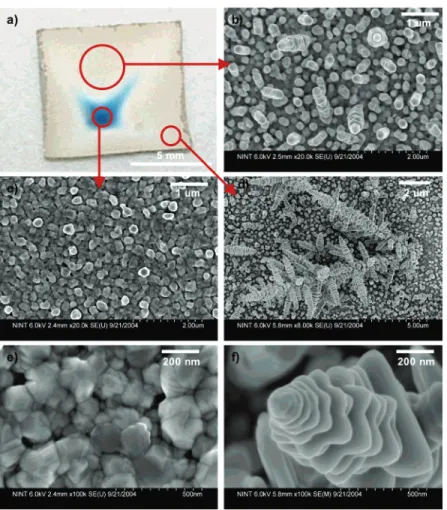
Figure 1. (a) A stone inukshuk in Northern Canada. (b) Silver nano-inukshuks formed by immersion of Ge(111) p-type in a 1.0 × 10⁻³M silver acetate (aq) for 4 h. (c) Nano-inukshuks prepared by immersion of Ge(111) p-type in 1.0 × 10⁻³ M silver nitrate
(aq) for 4 h.
Figure 2. (a) Silver nano-inukshuks prepared by immersing n-type Ge(100) in 1.0 × 10⁻³M AgNO
3(aq) for 4 h. (b) Close-up of
facets on the tips of silver metallic nano-inukshuks formed on p-type Ge(111) with 1.0 × 10⁻³M AgNO
3for 24 h.
local cathodic nature of the silver metal deposits;10bOCP
experiments indicate that if the edges are not exposed, the surface potential rises by 50-100 mV. Figure 4 shows an optical image of a 1 cm2germanium wafer, with SEM images
of different regions. The nano-inukshuks form across most of the face of the wafer, with the exception of the middle spot of the wafer, presumably the global anode as indicated by substantial germanium oxide deposits (by EDS) and little silver deposition, and the dendritic regions near the edges. Figure 5 provides a dramatic representation of the extended growth from the corners of the sample after an extended 24 h immersion of Ge(100) n-type in 1 mM AgNO3. The
dendrites reflect the hexagonal plate parent structure as determined by SEM (figures 5b and c). SEM images of silver-on-Ge samples with no edges appear much less ordered, with few nano-inukshuks and substantial tenacious germanium oxide deposits.
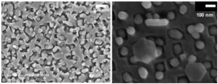
At concentrations below 0.5 mM silver ion, a combination of etching and metal deposition occurs, as represented by Figure 6 and the Supporting Information. At 1 × 10⁻⁴ M
AgNO3(aq), triangular and square etch pits with embedded
silver nanoparticles are observed on Ge(111) and Ge(100), respectively. At 10-5M AgNO
3(aq), etching of the
germa-nium alone is the predominant process. 10-4M silver ion
Figure 3. TEM of a silver hexagon isolated by sonication of silver nano-inukshuks in methanol. (a) TEM of a silver metallic hexagon; the black bar is 100 nm. (b) Selected area diffraction (SAED) pattern of the left 1/3 of this figure (omitting dark area). (c) Indexed hexagonal nanocrystal based on the SAED of (b). (d) Close-up of a nano-inukshuk tip for comparison; the white bar is 100 nm.
Figure 4. Demonstration of different regions of silver deposition across the face of a Ge(100) n-type wafer after 4 h, with 1.0 × 10⁻³M
AgNO3. (a) Optical photograph of a 1 cm diameter wafer, showing the X-shape and areas of silver deposition (light colored areas). (b) The
aligned nano-inukshuks form predominately on the flat planes across the front of the wafer, as shown in this SEM. (c,e) SEM images of the center of the X-shape; EDS indicates that this central area is made up of germanium oxide and some silver. (d,f) Toward the corners, dendritic structures are observed (SEM images).
appears to be the minimum concentration at which silver deposition on the surface competes effectively with etching. At higher concentrations of 10-2M silver ion, rapid silver
deposition occurs, leading to growth in ∼1 h of somewhat faceted silver dendritic structures on the surface.
The effects of the germanium wafer orientation, doping, choice of counteranion, additives, temperature, light, and stirring, were investigated and found to have small effects
on the galvanic displacement reaction. Wafer orientation is relatively unimportant for nano-inukshuk formation as they were observed on Ge(111) and Ge(100) faces, and even on the rough edges of germanium. Doping, n- or p-type, of the wafers does, however, affect the rate of deposition; optical images in the Supporting Information show that n-type wafers lead to faster overall deposition than p-type. Different Ag(I) salts also yield nano-inukshuks, including AgClO4and
Ag(CH3CO2), although with the former, deposition was more
rapid than with AgNO3. AgSO4, on the other hand,
consist-ently produced more flat dendritic structures. Consequconsist-ently, few generalizations concerning anion effects can be made at this point. Addition of an equivalent of sodium nitrate to the 1.0 mM AgNO3 reactions did little to change the
outcome, although there appeared to be more etching of the germanium. Since germanium oxides are produced via the galvanic displacement, it could be postulated that germanium oxide acts as a directing agent. The presence, however, of an excess of GeO2, purchased commercially, had only a
minor influence on a 1.0 mM AgNO3deposition except to
render the surfaces more difficult to analyze due to residual germanium oxides coating the nanostructures. Higher tem-peratures (40 °C) not surprisingly increase the deposition rate, but the silver is dendritic and more unstructured; lower temperatures (4°C) favor formation of flat plates. Illumina-tion of the reacIllumina-tions with white light irradiaIllumina-tion results in continuous metal deposition across the face of the wafer with substantial concomitant oxidation, but nano-inukshuks were clearly visible in most regions of the germanium wafer face. Stirring the solution has a subtle effect on silver deposition; vertical inukshuks are observed on the flat germanium face toward the edges, with the dendritic structures growing off the edge, but the X-pattern of the global anode becomes less obvious visually. These results point to a fine balance between diffusion and silver surface energetics that deter-mines the shape of the resulting structures.
To conclude, galvanic displacement of silver(I) ions leads to complex crystalline, metallic silver nanostructures on native oxide-coated germanium surfaces. Detailed electro-chemical studies of the electrodeposition process on germa-nium and other semiconductors are presently under inves-tigation to correlate structure, potential, and greater degrees of selectivity.
Acknowledgment. This work was supported by the National Research Council of Canada (NRC), the University
Figure 5. Long-term (24 h) deposition of silver nitrate leads to a large amount of dendritic deposition from the edges and corners of the Ge wafer. (a) Optical micrograph of Ge(100) n-type immersed in 1.0 × 10⁻³M silver nitrate. (b,c) SEM images of some of the
different dendritic structures observed on the edges of the germa-nium wafer; all reflect the parent hexagonal inukshuk shape.
Figure 6. 1.0 × 10⁻⁴ M silver nitrate deposition conditions,
demonstrating local etching of the germanium substrate induced by silver nanoparticle formation on the surface. (a) p-Type Ge(111) after 1 h deposition. (b) p-Type Ge(100) following 5 h of deposition.
of Alberta, the Department of Chemistry of the University of Alberta, NSERC, the Canadian Foundation for Innovation, and the Canada Research Chairs program (to J.M.B.). M.A. is an NSERC Visiting Fellow. A.M.C. was an undergraduate NRC intern from the University of New Brunswick, Canada. The authors wish to thank Isabella Pain for helpful discus-sions about inukshuks, Stephen Launspach and Daniel Solomon for assistance with the SEM, and Dr. Joel Haber for use of his electrochemical setup. Dr. Karim-Aly Kassam is thanked for the photographs of inukshuks in the Arctic.
Supporting Information Available: Detailed experi-mental procedures and characterization of the nano-inukshuks (XPS, XRD, EDS, SEM), SEM images of other conditions mentioned here not shown, and open cell potential (OCP) profiles. This material is available free of charge via the Internet at http://pubs.acs.org.
References
(1) (a) El-Sayed, M. A. Acc. Chem. Res. 2004, 37, 326. (b) Yin, Y. D.; Rioux, R. M.; Erdonmez, C. K.; Hughes, S.; Somorjai, G. A.; Alivisatos, A. P. Science 2004, 304, 711. (c) El-Sayed, M. A. Acc. Chem. Res. 2001, 34, 257. (d) Wang, J.; Tian, M.; Mallouk, T. E.; Chan, M. H. W. J. Phys. Chem. B 108, 841-845.
(2) (a) Puntes, V. F.; Zanchet, D.; Erdonmez, C. K.; Alivisatos, A. P. J. Am. Chem. Soc. 2002, 124, 12874. (b) Puntes, V. F.; Krishnan, K.; Alivisatos, A. P. Top. Catal. 2002, 19, 145.
(3) Kim, F.; Connor, S.; Song, H.; Kuykendall, T.; Yang, P. Angew. Chem. Int. Ed. 2004, 43, 3673.
(4) (a) Prodan, E.; Radloff, C.; Halas, N. J.; Nordlander, P. Science 2003, 302, 419. (b) Chen, S.; Wang, Z. L.; Ballato, J.; Foulger, S. H.; Carroll, D. L. J. Am. Chem.. Soc. 2003, 125, 13186. (c) Charnay, C.; Lee, A.; Man, S.-Q.; Moran, C. E.; Radloff, C.; Bradley, R. K.; Halas, N. J. J. Phys. Chem. B 2003, 107, 7327. (d) Sau, T. K.; Murphy, C. J. Langmuir 2004, 20, 6414. (e) Wang, Z. L.; Gao, R.; Nikoobakht, B.; El-Sayed, M. A. J. Phys. Chem. B 2000, 104, 5417. (5) Jin, R.; Cao, Y.; Mirkin, C. A.; Kelly, K. L.; Schatz, G. C.; Zheng,
J. G. Science 2001, 294, 1901.
(6) (a) Sun, Y.; Xia, Y. Science, 2002, 298, 2176. (b) Yu, D.; Yam, V. W.-W. J. Am. Chem. Soc. 2004, 126, 13200.
(7) (a) Caswell, K. K.; Bender, C. M.; Murphy C. J. Nano Lett. 2003, 3, 667. (b) Tian, M.; Wang, J.; Kurtz, J.; Mallouk, T. E.; Chan, M. H. W. Nano Lett. 2003, 3, 919-923.
(8) (a) Germain, V.; Li, J.; Ingert, D.; Wang, Z. L.; Pileni, M. P., J. Phys. Chem. B 2003, 107, 8717. (b) Maillard, M.; Giorgio, S.; Pileni, M.-P. J. Phys. Chem. B 2003, 107, 2466.
(9) Oskam, G.; Long, J. G.; Natarajan, A.; Searson, P. C. J. Phys. D: Appl. Phys. 1998, 31, 1927.
(10) (a) Magagnin, L.; Maboudian, R.; Carraro, C. J. Phys. Chem. B 2002, 106, 401. (b) Niwa, D.; Homma, T.; Osaka, T. J. Phys. Chem. B
2004, 108, 9900. (c) Lin, H.; Mock, J.; Smith, D.; Gao, T.; Sailor, M. J. J. Phys. Chem. B 2004, 108, 11654. (d) Porter, L. A., Choi, H. C. Buriak, J. M. Nano Lett. 2002, 2, 1067. (e) Zambelli, T.; Munford, M. L.; Pillier, F.; Bernard, M.-C.; Allongue, P. J. Electrochem. Soc.
2001, 148, C614. (f) Harraz, F. A.; Tsuboi, T.; Sasano, J.; Sakka, T.; Ogata, Y. H. J. Electrochem. Soc. 2002, 149, C456. (g) Sun, X.-H.; Wong, N.-B.; Li, C.-P.; Lee, S.-T.; Kim, P.-S. G.; Sham, T.-K. Chem. Mater. 2004, 16, 1143. (h) Takano, N.; Niwa, D.; Yamada, T.; Osaka, T. Electrochim. Acta 2000, 45, 3263. (i) Kim, C.; Oikawa, Y.; Shin, J.; Ozaki, H. Microelectron. J. 2003, 34, 607. (j) Gorostiza, P.; Allongue, P.; Dı´az, R.; Morante, J. R.; Sanz, F. J. Phys. Chem. B 2003, 107, 6454.
(11) The solubility of GeO2in cold water is 10 g/L. Glockling, F. The
Chemistry of Germanium; Academic Press: London, 1969. NL048008K