Arrayed Microfluidic Actuation for Active Sorting
of Fluid Bed Particulates
by
Antimony L. Gerhardt
S.B., Electrical Science and Engineering Massachusetts Institute of Technology, 2003
Submitted to the Department of Electrical Engineering and Computer Science in Partial Fulfillment of the Requirements for the Degree of
Master of Engineering in Electrical Engineering and Computer Science at the
Massachusetts Institute of Technology December 2003
C 2003 Massachusetts Institute of Technology. All rights reserved.
I A
MASSACHUSETTS INS OF TECHNOLOGY E
LIBRARIES
Signature of Author
Departm t of Elec ffical Elgineering and Computer Science December 3, 2003
Martin A. Schmidt Professor of Electrical Engineering and Computer Science Thesis Supervisor
rtha L. Gray Edward Hood Taplan Professor of Electric Engineering Thesis Supervisor
Certified by
Mehmet Toner Professor of Biomedical Engineering, Harvard Medical School, and Massachusetts General Hospital
1--/' -- Thesis Supervisor
Accepted by
Arthur C. Smith
Chairman, Department Committee on Graduate Theses IWASSACHUSETT INS
OF TECHNOLOGy
Certified by
Certified by
Arrayed Microfluidic Actuation for Active Sorting
of Fluid Bed Particulates
by
Antimony L. Gerhardt
Submitted to the Department of Electrical Engineering and Computer Science December 3, 2003, in Partial Fulfillment of the Requirements for the Degree of
Master of Engineering in Electrical Engineering and Computer Science
Abstract
Fluidic actuation offers a facile method to move large quantities of small solids, often referred to as fluid-bed movement. Applications for fluid bed processing are integral to many fields including petrochemical, petroleum, chemical, pharmaceutical, biochemical, environmental, defense, and medical. Thermal vapor microbubbles have been shown to be a
low power input with high work output fluidic actuation technique with demonstrated commercial applications in ink jet printing and optical switching.
This thesis further develops microbubble actuation (1iBA) as an arrayed particulate actuation technology for active sorting in particulate fluid beds. Numerical and analytical models of flows, forces, and fields affecting a piBA-based system are presented. The design and
fabrication of an arrayed pBA-powered device are delineated with notation of specifications that may focus future design iterations. Performance testing and characterization of pBA technology, including over a hundred in-plane and out-of-plane nucleation site geometries,
serve as the impetus for the technical guidelines that are presented, which include a detailed comparison of in-plane and out-of-plane nucleation site geometry performance.
Thesis Supervisor: Martin A. Schmidt
Title: Professor of Electrical Engineering and Computer Science Thesis Supervisor: Martha L. Gray
Title: Edward Hood Taplan Professor of Electrical Engineering Thesis Supervisor: Mehmet Toner
Title: Professor of Biomedical Engineering, Massachusetts General Hospital, and Harvard Medical School
Acknowledgements
A book seems to sit idly on a shelf awaiting a reader to bring it to life. In kind, research awaits individuals to give it breath and spirit through hours of contemplation, computation, and labors of love. This research was realized with the guidance of many hands and many hours.
The advisors of the gDAC committee - Marty Schmidt, Martha Gray, and Mehmet Toner - were instrumental to the research. Marty was a crucial resource, offering a research family to me almost as soon as I stepped foot on campus. With his guidance, progress became a constant rather than a wish. In-depth discussions with Martha at the Alliance for Cellular Signaling (AfCS) 3rd Annual Meeting and throughout the research progression focused the objectives of the next-generation pBA-powered device and the future generation outlined in the concluding sections of this thesis. Mehmet served as an invaluable editor,
link to existing technologies in the field, and resource in the development of the biological component of the pBA-powered device.
We are most grateful to Surface Technology Systems (STS) and their representatives Andrew Tucker and Phil Jones for their willingness to work toward developing future technologies by donating the etching of the quartz wafers in the UK. Also, MicroChem
representative Rob Hardman was quite helpful in providing information and data during the development of a successful, thick SU-8 process. The research was funded by the Alliance for Cellular Signaling, NIH grant number U54 GM62114, and the Edward Hood Taplin Professorship. The Ida M. Green Fellowship supported my graduate expenses.
The MTL family was an integral research component. Many thanks go to Vicky Diadiuck who gave process guidance both before and during fabrication. Dan Adams, Bernard Alamariu, Kurt Broderick, Gwendolyn Donahue, Dave Terry, Paul Tierney, Li-Wen Wang, and Dennis Ward were supporters throughout, training me and helping troubleshoot ICL, TRL, and EML equipment at all hours. Past and current members of the Schmidt Group shared thoughts, comments, and ideas as research progressed. Hang Lu and Saif Khan provided insight into thin SU-8 processing. Larry She of Shell Exploration & Production Company assisted early in the heat transfer modeling. And, Nicolas Szita lent the laser and expertise to laser print the alignment jig.
Others whose paths have crossed my own contributed in many ways. Special thanks go to the MIT extended community; Luis Lopes who helped me realize that dreams are never lost, ... only rewritten; Katherine Pedersen who has inspired me since first we met and is now a tremendous mentor and friend; Rai Weiss who taught me how to do real research; Steve Senturia and Mike Butler who taught me how to develop industry-applicable designs and devices; and Kent and Gwendolyn Gerhardt, my extended family, the PEOs, and the Victoria and Hammond communities who have supported me through every triumph and test of health and character.
Contents
C hapter 1 Introduction ... 23 1.1 Background ... 23 1.1.1 M icrofluidics ... 23 1.1.2 BioM EM S... 27 1.2 M otivation... 291.2.1 Microfabrication-based Dynamic Array Cytometer ... 29
1.2.2 Conceptual pDA C System ... 31
1.2.3 pDAC Progress... 32
1.2.4 uBA D evice Concept ... 33
1.3 Objective ... 36
1.4 Scope... 37
1.5 References... 38
Chapter 2 Theoretical Properties of Microbubbles ... 47
2.1 V apor Bubbles ... 47
2.1.1 Pool Boiling ... 47
2.1.2 H eterogeneous N ucleation... 48
2.1.3 Growth and D issipation M echanisms ... 49
2.2 System Parameters Affecting Vapor Bubble Formation ... 51
2.2.1 Surface Properties ... 51
2.2.2 System Properties... 54
2.3 References... 54
Chapter 3 Flow s, Forces, and Fields... 57
3.1 In-Plane H eat Flow ... 57
3.1.1 Finite-Difference Model of Steady Conduction ... 58
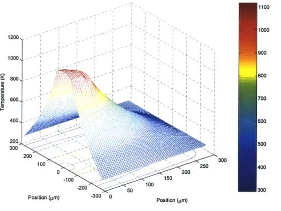
3.1.2 Numerically Simulated Temperature Distributions ... 61
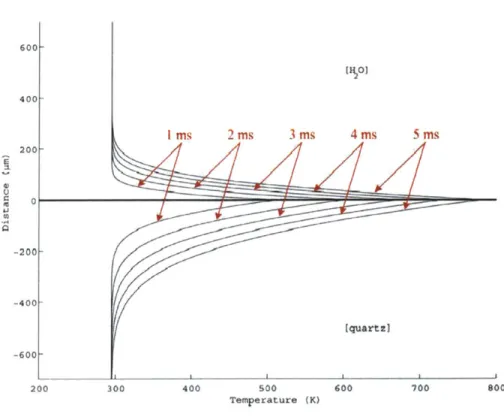
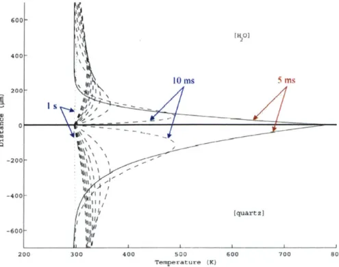
3.2 O ut-of-Plane H eat Flow ... 68
3.2.1 Analytical M odel of Transient Conduction... 69
3.2.2 Analytically Simulated Temperature Distributions ... 75
3.3 Ejection Force ... 79
3.5 D iscussion... 87
3.6 References... 88
Chapter 4 Design and M anufacture ... 91
4.1 Specifications... 91
4.1.1 Processing Time ... 91
4.1.2 Optical Interface ... 92
4.1.3 Reliability and Robustness ... 93
4.1.4 Ease of Operation ... 93
4.1.5 Cost Effectiveness ... 93
4.1.6 Compatibility... 94
4.2 System Architecture... 94
4.2.1 Platinum H eating Electrode Chip... 96
4.2.2 Test Structure Chip ... 99
Test Structure Chip v3.0 ... 99
Test Structure Chip v3.I ... 100
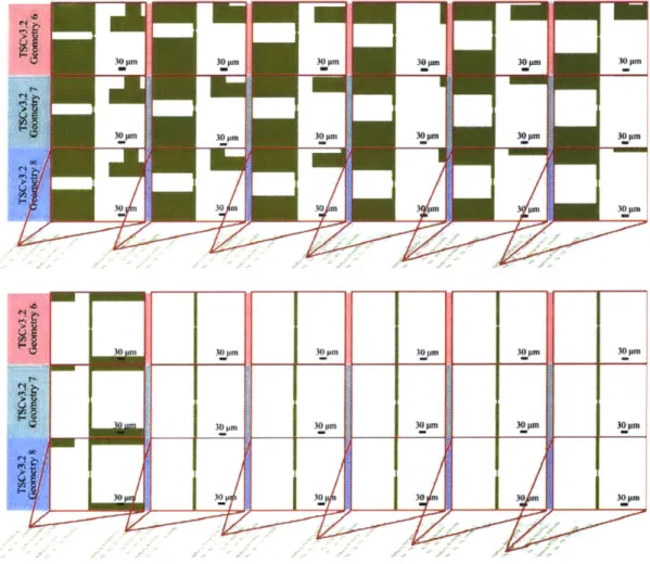
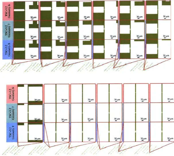
Test Structure Chip v3.2 ... 102
4.2.3 Fluidic System ... 109
4.2.4 Electronic Interface ... 111
4.3 M icrofabrication ... 114
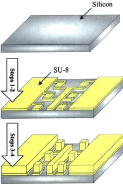
4.3.1 Platinum H eating Electrode Chip... 114
4.3.2 Test Structure Chip ... 118
4.3.3 D eionized Header M old... 121
4.3.4 Input M edium H eader M old... 124
4.3.5 M icrofabrication Challenges... 127
4.4 A ssem bly and Packaging ... 128
4.4.1 Assem bly and Packaging Process... 128
4.4.2 Assem bly and Packaging Challenges ... 132
4.5 References... 133
Chapter 5 Perform ance...135
5.1 Hypotheses... 135
5.1.1 Control of M icrobubble Shape and Location ... 135
5.1.2 Regulation of M icrobubble Size ... 136
5.1.3 Regulation of M icrobubble Dissipation... 136
5.2 M ethods... 136
5.2.1 Experim ental Apparatus ... 136
5.2.2 M icroscope-to- Video M easurement Calibration ... 140
5.2.3 Resistor Element Values ... 140
5.2.5 Eccentricity ... 142
5.2.6 Centricity... 143
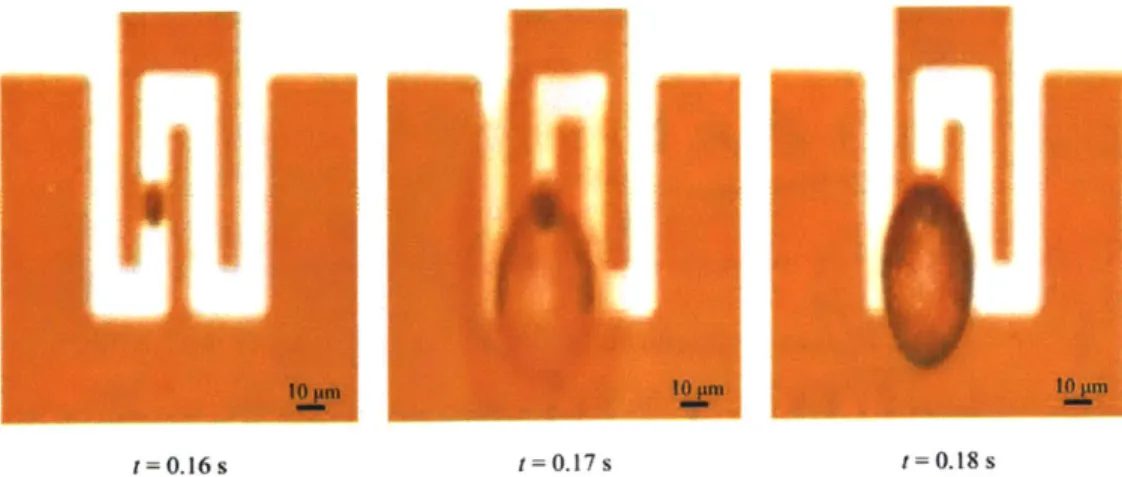
5.2.7 Transient D iameters... 144
5.2.8 Transient D issipation Times ... 147
5.3 Results... 150
5.3.1 Archetypal Curves... 150
5.3.2 M icrobubble Shape and Location... 156
5.3.3 M icrobubble Size ... 158
5.3.4 M icrobubble D issipation ... 159
5.3.5 Performance Comparison of Out-of-Plane and In-Plane Geometries ... 161
5.3.6 D rift... 167
5.3.7 Rapid Cycling... 168
5.4 References... 173
C hapter 6 D iscussion and C onclusions ... 175
6.1 Perform ance D iscussion... 175
6.1.1 Control of M icrobubble Shape and Location ... 175
6.1.2 Regulation of M icrobubble Size ... 176
6.1.3 Regulation of M icrobubble D issipation... 177
6.2 Com parison of O ut-of-Plane and In-Plane Perform ance ... 178
6.3 Recommendations, Future Work, and Potential Applications... 182
6.4 References... 183
A ppendix A Fabrication Process Flow s... 185
A ppendix B M ask Design ... 191
B.1 Platinum H eating Electrode Chip... 192
B.2 Test Structure Chip... 195
B.3 D eionized H eader M old ... 198
B.4 Input M edium H eader M old... 207
A ppendix C Electrical Schem atic Diagram s... 215
List of Figures
Figure 1-1. Inkjet Printing ... 24
Figure 1-2. Optical Switching... 25
Figure 1-3. uBA-Based Components. ... 26
Figure 1-4. Microscopy and Flow Cytometry... 30
Figure 1-5. Conceptual uDAC System... 32
Figure 1-6. Early DEP-Powered uDAC Efforts ... 33
Figure 1-7. Early piBA Capture Site ... 34
Figure 1-8. Early pBA Capture and Release Schematic... 35
Figure 1-9. Early pBA Fabricated Chip ... 36
Figure 1-10. First-Generation Package ... 36
Figure 2-1. Boiling Regimes...48
Figure 2-2. Bubble Cycle and Induced Flow Patterns ... 50
Figure 2-3. Effect of Surface Wettability on Contact Angle ... 52
Figure 2-4. Gas Entrapment Criterion ... 53
Figure 3-1. uBA-Based Components ... 57
Figure 3-2. Finite Control Volume ... 58
Figure 3-3. Nodal Meshes for Steady Conduction in Resistor Geometries ... 60
Figure 3-4. Composite Conduction in Resistor Geometries ... 63
Figure 3-5. Temperature Distribution in Linear Resistor with Gp, GQ ... 64
Figure 3-6. Temperature Distribution in Linear Resistor with Gp, # GQ ... 65
Figure 3-7. Temperature Distribution in Serpentine Resistor with Gp, = GQ... 66
Figure 3-8. Temperature Distribution in Serpentine Resistor with Gp, t GQ ... 67
Figure 3-10. Heating Out-of-Plane Temperature Profile for Fixed q ... 77
Figure 3-11. Cooling Out-of-Plane Temperature Profile for Fixed q, ... 78
Figure 3-12. Schematic Diagram for Particle Ejection Force... 80
Figure 3-13. Bubble Formation on Serpentine Resistor with Etched Cavity ... 82
Figure 3-14. M agnetic Field Lines and Amplitudes for R = 10 Q ... 86
Figure 3-15. M agnetic Field Lines and Amplitudes for R = 100 Q ... 86
Figure 4-1. System Architecture ... 95
Figure 4-2. PHE Chip ... 97
Figure 4-3. PHE Chip Pad Designations ... 97
Fi gure 4-4. TSC Iterations ... 99
Figure 4-5. TSCv3.0 Geometrical Variations ... 100
Figure 4-6. TSCv3.1 ... 101
Figure 4-7. TSCv3.1 Geometrical Variations ... 102
Fi gure 4-8. TSCv3.2 Chips ... 103
Figure 4-9. TSCv3.2 Geometries 1-4 ... 104
Figure 4-10. TSCv3.2 Geometry 5 ... 104
Figure 4-11. TSCv3.2 Geometries 6-8 with Shared Ground ... 105
Figure 4-12. TSCv3.2 Geometries 6-8 with Independent Ground ... 106
Figure 4-13. TSCv3.2 Geometry 9 ... 108
Figure 4-14. Particulate-Level Fluidic System ... 109
Figure 4-15. Lumped Element M odel of Fluidic System ... 110
Figure 4-16. M M I Design ... 111
Figure 4-17. M anufactured M M I... 112
Figure 4-18. UIM Design ... 113
Figure 4-20. PHE Chip Pictorial Process Flow ... 116
Figure 4-2 1. SEM s of Nucleation Site ... 117
Figure 4-22. TSC Pictorial Process Flow ... 119
Figure 4-23. Fabricated TSCv3.0 Wafer ... 120
Figure 4-24. Fabricated TSCv3.1 Wafer ... 120
Figure 4-25. Fabricated TSCv3.2 Wafer ... 121
Figure 4-26. DI Header M old Pictorial Process Flow... 122
Figure 4-27. Thick Photoresist Alignment M arks ... 123
Figure 4-28. Fabricated DI Header M old ... 124
Figure 4-29. IM Header M old Pictorial Process Flow ... 125
Figure 4-30. Fabricated IM Header M old... 127
Figure 4-31. pBA Device Assembly ... 129
Figure 4-32. PDM S Alignment Jig ... 130
Figure 4-33. Fluidically PackagedpBA -Based Device ... 131
Figure 4-34. Fluidically Packaged uBA-Based Device... 132
Figure 5-1. System Architecture ... 137
Figure 5-2. TSC Electrical Contact Scheme ... 138
Figure 5-3. Illustration of PDM S Gasket on TSC... 139
Figure 5-4. Photograph of PDM S Gasket on TSC... 139
Fi gure 5-5. Standard Input ... 141
Figure 5-6. Chirped Input... 141
Figure 5-7. Eccentricity...142
Fi gure 5-8. Centricity ... 143
Figure 5-11. Figure 5-12. Figure 5-13. Figure 5-14. Figure 5-15. Figure 5-16. Figure 5-17. Figure 5-18. Figure 5-19. Figure 5-20. Figure 5-21. Figure 5-22. Figure 5-23. Figure 5-24. Figure 5-25. Figure 5-26. Figure 5-27. Figure 5-28. Figure 5-29. Figure 5-30. Figure 5-3 1. Figure 5-32. Figure 5-33. Figure 5-34. Figure A-1.
Transient D issip ation Tim es... Fast Transient Dissipation Micrographs ... Slow Transient Dissipation Micrographs... Complete System Response for Resistor with 10 pm Nucleation Site ... Complete System Response for Resistor with 20 pm Nucleation Site ... Complete System Response for Resistor with 30 pm Nucleation Site ... Complete System Response for 7 Q Resistor...
Representative Chirped Input Maximum Diameter Curve ... Representative Slow Transient td Curve ...
Representative Slow Transient Max Average Diameter vs. td Curve ...
In-Plane Microbubble Shape and Location ... In-Plane Slow Transient Maximum Microbubble Size ... In-P lane Slow Transient td ... In-Plane Slow Transient Microbubble Size vs. td...
Complete System Response for Out-of-Plane Geometry ... Out-of-Plane and In-Plane Microbubble Shape and Location ... Out-of-Plane and In-Plane Slow Transient Maximum Microbubble Size ... Out-of-Plane and In-Plane Slow Transient td ... Out-of-Plane and In-Plane Slow Transient Microbubble Size vs. td ... D rift... Rapid Cycling Out-of-Plane Geometry Resistor ... Rapid Cycling In-Plane Geometry Resistor with 10 pm Nucleation Site ... Rapid Cycling In-Plane Geometry Resistor with 20 pm Nucleation Site ... Rapid Cycling In-Plane Geometry Resistor with 30 pm Nucleation Site ... PHE Chip Delineated Process Flow ...
147 148 149 150 151 152 153 154 155 156 157 159 160 161 162 163 165 166 167 168 169 170 171 172 186
Figure A -2. TSC Chip D elineated Process Flow ... 187
Figure A -3. DI H eader M old D elineated Process Flow ... 188
Figure A -4. IM H eader M old D elineated Process Flow ... 189
Figure B-1. PH E Chip M ask I ... 192
Figure B-2. PH E Chip Alignment M ark ... 193
Figure B-3. PH E Chip M ask 2 ... 194
Figure B-4. TSCv3. M ask 2 ... a0 195 Figure B-5. TSCv3.1 M ask 2 ... 196
Figure B-6. TSCv3.2 M ask 2 ... 197
Figure B-7. DI H eader M old Right Alignment M ark ... 198
Figure B-8. H eader M old 2xM ask I ... 199
Figure B-9. H eader M old Alignm ent M ark ... 200
Figure B-10. H eader M old xM ask I ... 201
Figure B-11. D I H eader M old 2xM ask 3 ... 202
Figure B --12. H eader M old Upper Alignment M ark ... 203
Figure B-13. DI H eader M old Fluidic H ub... 204
Figure B-14. DI H eader M old I x M ask 3 ... 205
Figure B-1 5. DI H eader M old 2 x M ask 4 ... 206
Figure B-16. DI H eader M old Ix M ask 4 ... 207
Figure B-17. IM H eader M old 2 x M ask 7... 208
Figure B --18. IM H eader M old I x M ask 7 ... 209
Figure B --19. IM H eader M old 2 x M ask 6... 210
Figure B-20. IM H eader M old I x M ask 6... 211
Figure C-1. PHE Chip Electrical Schematic ... 215
Figure C-2. Fluidic System Lumped Element M odel Electrical Schematic ... 216
Figure C-3. PHE Chip Electrical Schematic ... 217
Figure C-4. MM I Electrical Schematic ... 218
Figure C-5. UIM Electrical Schematic ... 219
List of Tables
Table 1-1. Attribute Comparison of Microscopy, Flow Cytometry, and pDAC ... 31
Table 3-1. Change in Temperature at y = 300 ,m for Variable q ... 79
Table 4-1. Fluidic Dimensions and Calculated Poiseuille Lumped Element Values ... 111
Table 6-1. Comparison of Out-of-Plane and In-Plane Resistor Geometries ... 179
Table D-1. Sampling of Raw Data for IP Resistor with 10 pm Nucleation Site ... 223
Table D-2. Sampling of Raw Data for IP Resistor with 20 pm Nucleation Site... 224
Table D-3. Sampling of Raw Data for IP Resistor with 30 pm Nucleation Site ... 224
Nomenclature
a A b B B Cnb C d e D E fA F G G Gn hfg H K N m n L P P semi-major axis, in constant; area, m2 semi-minor axis, m magnetic field, T magnetic field vector, T constant in nucleate boiling correlation centricity ratio diameter, m; distance, m eccentricity ratio diameter, in cardinal direction pulse frequency, Hz force, N conductance, Siemens conductance matrix, Siemens conductance between nodes in then directions, Siemens
enthalpy of vaporization, J/kg height, m; thickness, in node; current, A current, A
pressure gradient, Pa-m cardinal direction coordinate; slope coordinate
sampling length; length, m; characteristic length, m power, W
pressure, Pa
P power density, W/m3
q heat flux, W/m2
Q
volumetric flow rate, m3/sQ
rate of heat transfer into system, rate of heat flow, WQ-
internal heat source, WQ,
volumetric heat source per unit volume, W/m3r radius, m r radius vector, m
R electrical resistance, Q; thermal resistance, K/W
Ra average roughness, m
Rn thermal resistance between nodes in the n directions, K/W
R, thermal resistance between nodes in the x direction, K/W
R, thermal resistance between nodes in the y direction, K/W
RPOs fluidic resistance, Pa-s/m 3
Re Reynolds number s length, m s length vector, m S cardinal direction t time, s tq time of q termination, s T temperature, K T temperature matrix, K
U mean flow velocity, m/s
V volume, m3; voltage, V W cardinal direction; width, m
y rectangular coordinate, m; elevation, m z rectangular coordinate, m; elevation, m Greek Symbols a thermal diffusivity, m2/s 6 pulse width, s
bt temperature penetration depth, m A finite increment; thermal boundary
layer thickness, m; time between pulse wavefronts, s
A T, excess temperature, K 6 angle, rad; contact angle, 0
K thermal conductivity, W/m-K P viscosity, Pa-s P* kinematic viscosity, m3/s Po permeability constant, H/m variable of integration Pe electrical resistivity, 92-m PM mass density, kg/m3
PV saturated vapor density, kg/m3 Ost surface tension of liquid-vapor
interface, N/in
V/min angle between sidewall of cavity and heating surface,
Subscripts c cavity, constant ch channel d development, dissipation D hydraulic diameter DI deionized header CS e eq eject g h IM I IM in
I
L ns 0 out p P Pt p1Q
r S SA sat Ti w W cross section ellipsoid equivalent ejection gravity hydraulic node interface input medium inlet jet linear nucleation site initial outletparticle; particular solution point of observation platinum power lead quartz resistor serpentine surface area saturated titanium
surface; solid wall water
Diacritics
Acronyms
AfCS Alliance for Cellular Signaling
A OE advanced oxide etcher
BioMEMS biological microelectromechanical systems
MEMS microelectromechanical systems
MTL Microsystems Technology Laboratories
DC direct current
DEP dielectrophoresis
DI deionized
DNA deoxyribonucleic acid
dpi dots per inch
EML Exploratory Materials Laboratory HMDS hexamethyldisilazane
IC integrated circuit
ICL Integrated Circuits Laboratory
IM input medium
IP in-plane
IR infrared
LPCVD low pressure chemical vapor deposition
MMI macro-to-micro interface
NIH National Institutes of Health
OP out-of-plane
PDMS polydimethylsiloxane
PHE platinum heating electrode
RF radio frequency
SEM scanning electron microscope, scanning electron micrograph
TRL Technology Research Laboratory
TSC test structure chip
UIM user interface module
pBA microbubble actuation
Chapter 1
Introduction
1.1 Background
Macro fluidic actuation is the use of mechanical devices to move or control fluids. Fluidic actuation yields a mechanical advantage in hydraulic systems utilizing pistons and serves as a facile method to move large quantities of small solids, often referred to as fluid bed movement. Integrating fluidic actuators, then, with sensors and distribution channels offers the ability to process significant amounts of solid materials entrained in a fluid flow. Mass production processing such as sorting, aerating, moving, drying, cooling, granulation, and coating of thermally sensitive and insensitive particulates can be accomplished at a commercial level using this fluid bed movement. Applications are integral to many fields including petrochemical, petroleum, chemical, pharmaceutical, biochemical, environmental, defense, and medical [1, 2].
1.1.1 Microfluidics
An extension of macro fluidics was made possible by the microelectromechanical systems (MEMS) revolution. Miniaturized macro fluidics, microfluidics, has applications for many small-particulate handling and processing systems as liquids and entrained particles can be handled more precisely [3-5]. A completely integrated micro fluid handler inherently has faster response times, smaller dead volumes, reduced sample sizes, and higher
throughputs. Flow can be sensed and controlled on the order of 1 pl/min, and devices can be paired with microsensors to enable feedback control [6]. Higher precision sensing and control will allow greater reliability and repeatability. Additionally, miniaturized flow devices can be batch processed at a lower cost than the macro counterparts and are inherently more portable.
The benefits of moving from the macro to micro fluid bed regimes have inspired research in microflow components - actuators [7-9], valves [9-14], pumps [15-18], ducts [19], mixers [20-22], switches [23, 24], sensors [25-29], and others such as heat-exchangers, reactors, motors, and flow controllers. These building block components then are integrated
Arrayed Microfluidic Actuation for Active Sorting of Fluid Bed Particulates
to produce more complex systems such as microflow devices. Commercial applications of microflow technology include industrial gas and liquid control systems, chemical analysis, whole blood preparation systems, drug targeting, gene therapy, bioreactors, particle counting
and sorting, and inkjet printers [10, 22, 30-32].
Commercially successful, inkjet printing is based on the concept of using a resistor to heat approximately 0.3% of the ink in a chamber [33, 34]. The heated ink vaporizes. The expansion displaces surrounding ink, and some of the displaced ink is ejected out of the printer nozzle. The ejected ink prints on a sheet of paper. As the vapor bubble collapses, a vacuum is created that pulls the remaining ink back into the cartridge. The dots per inch (dpi) resolution of a printer is determined by the size of the ejected droplet and the spacing between nozzles in the array. Because the thermally formed bubble ejects the ink, inkjet printers are often called bubble jet or thermal printers. Figure 1-1 illustrates ink ejecting from a nozzle of an inkjet printer head.
Figure 1-1. Inkjet Printing. (Copyright of Hewlett-Packard Company; used with permission.)
The mechanism behind inkjet printing can be assorted as thermal actuation,
microbubble actuation (pBA), or the phenomenon of boiling. Compared with other actuation technologies such as electromagnetic, electrostatic, thermal bimetallic, and piezoelectric, pBA can be accomplished with a design that requires no mechanical moving parts and relatively simple electronics [35]. pBA is not prone to mechanical failure resulting from
Chapter 1 Introduction
fatigue and fabrication defects like other actuation techniques, and relatively low power inputs generate large forces. Microbubbles can be nucleated in open or controlled
environments [3]. Further, as inkjet printing demonstrates, the pBA technology is scalable, robust, and can be cost effective enough to be commercialized.
The same bubble mechanism used in inkjet printing was shown to be commercially viable as an optical switch [36, 37]. Using the high-reflectivity bubble as a pseudo-mirror, Agilent Technologies developed a printed circuit where multiple wave guides intersect at critical cross points. The cross points contain fluids with the same optical characteristics as the waveguide. A bubble nucleated at a cross point redirects the light along a new path, switching information in a fast and reliable manner with no mechanical parts. Figure 1-2 depicts this optical bubble technology device, which was dubbed Champagne because of the similarity between a thermally formed microbubble and the minute bubbles in a glass of champagne. At the center of the image is the cross point, where light currently is being redirected by a microbubble.
Figure 1-2. Optical Switching [361.
The development of integrated circuit (IC) technology led to the advent of extremely smooth surfaces. With glabrous microscale geometries, research of boiling phenomena
Arrayed Microfluidic Actuation for Active Sorting of Fluid Bed Particulates
bubble nucleation has been found to be a much more powerful process in the
microdimensions, as the potential to do work is greater. A large effort has been invested in the study of the microscale mechanism of boiling phenomena - formation, dissipation, and applications of thermally formed microbubbles [3, 34, 35, 38-53].
In addition to the largest commercial application of inkjet printing and the ongoing research to improve the process, a pBA DNA ejection device, an extension of current inkjet printing technologies, expels DNA creating a microarray for biological screening [54]. Other potential applications for pBA-powered systems include fluid mixing for chemical analysis, prime movers in micro steam engines, and integrated cooling for ICs. Additionally
improvements in bubble jet printing such as eliminating satellite ink drops [30, 31] and increasing resolution by decreasing fluidic ejection volumes are current areas of focus in pBA research.
pBA-based components such as micropumps, microdrop valves, flow controllers, mixers, microinjectors, check-valves, filters, and diffusers are in the research and
development stages [44, 55, 56].
(a) (b) (c)
Figure 1-3. pBA-Based Components.
Figure 1-3 illustrates a portion of one pBA-based device and two pBA-based components. The image in column (a) is a pair of microchannels. The forefront microchannel contains a bubble that has been formed to temporarily stop the flow of fluid. A bubble in the
Chapter 1 Introduction
component in (b) is a caricature of an inkjet printer nozzle, and a bubble-powered mixer is shown in (c).
1.1.2 BioMEMS
Microfluidics and other subdivisions of MEMS research have resulted in commercial applications ranging from bubble jet printers and later high-resolution inkjet-based color printers to accelerometers for air bags in the automotive industry [57]. In tandem, a field of MEMS coined Biological MEMS (BioMEMS) has emerged. BioMEMS devices have an enormous global market and the potential to dramatically alter current health care practice and research by serving as a supplement to current macro technologies.
The advantages of using MEMS in biology and medicine are vast [58]. MEMS mean the ability to maintain small device size, allowing the use of microscale phenomenon such as pBA. High surface-area-to-volume ratios enhance surface physical effects, such as heat dissipation. Thus, greater temperatures can be obtained without the adverse heating effects often encountered in the macro regime. Electronic integration can abate the overall device size, increase electromagnetic compatibility, improve reliability between interconnections, and potentially decrease production costs [57].
The "velocity" in units of cells or samples per second, throughput, is often the rate-limiting factor in biological research. The number of samples that can be read on a
spectrophotometer or the number of cells that can be analyzed and sorted in a flow cytometer in a given time determines, to a great extent, the amount of time required to perform an assay. The high throughput potential of MEMS, processing samples in massive
parallelization on a micro scale, promises drastically faster analysis.
Small sample volumes increase the usability of each histological sample, decrease the size requirement for medical diagnostics in which the sample material is scarce, reduce costs per assay especially when expensive reagents are involved, and can be used to deliver more precise dosages for chemotherapy and other treatments. Batch processing permits multitudes of devices to be created as simply as one. Thus, batch processing is cost effective and reduces device-to-device inconsistencies present in most macro construction. Geometrical
Arrayed Microfluidic Actuation for Active Sorting of Fluid Bed Particulates
control also allows interaction between tissues, cell, or other biological components to be carefully regulated.
Small device size, high surface-area-to-volume ratio, electronic integration, high throughput, small sample volume, batch processing, and geometrical control are some of the advantages MEMS technology can offer biomedicine. Researchers predict that the medical applications resulting from BioMEMS devices are a multi-billion dollar market [59]. Until recently, however, the focus of MEMS research was toward industrial rather than medical applications.
MEMS applications in biomedicine include sample handling using microdroplet generators [60]. Microdroplet generators for biomedical and chemical sample handling for mass spectrometry have been demonstrated by [61] and [62]. The objective of the devices is to output liquid samples such as DNA or proteins in a controlled fashion that increases the performance of the mass spectrometry system. A variation of microdroplet dispensers, conceptually similar to the inkjet printing method, have been used by [63]. High-density gene arrays were printed with 300 dpi resolution onto hybridization membranes and
hybridized with specific genes or total cDNA as probes. More complex microarrays could be created to facilitate hybridization of larger quantities of genes.
Another application of microsystems in medicine is using biosensors in functional assays ranging from receptor and ligand interaction characterization, toxicology, and chemotherapeutic agent evaluation [64, 65]. Biosensors are also used for blood-gas monitoring and in electrolyte sensing [66]. Information about physiological changes in cultured cells can be obtained using microphysiometry, and cell flow characteristics have been studied using microdevices. Drug targeting and gene therapy [32] as well as implantable devices [59] are other uses of BioMEMS devices and systems. Implantable devices, consisting of sensors and integrated processing electronics, could be used for biotelemetry, providing medical practitioners additional information for diagnostics and treatment.
Most biological applications of MEMS depend heavily on microfluidics. The
Chapter 1 Introduction
receptor ligand interaction are submerged in a fluidic medium. Blood-gas monitoring
systems draw microliters of blood, analyze the volume for gas content, and return the fluid to the patient.
Because BioMEMS involves mircofluids, refining current microfluidic technology is crucial to the advancement of BioMEMS devices and systems. To achieve higher precision sensing and control micosystem devices, the fluid-bed movement of fluids and particles can be studied and current methods of actuation and control can be developed further. With fluidic components created with greater accuracy, higher levels of control and predictability can be achieved, yielding results, devices, and systems that are more reliable, repeatable, and robust.
1.2 Motivation
Thermal vapor microbubbles have been shown to be a low power input with high work output fluidic actuation technique with applications in thermal bubble printing, as prime movers in micro steam engines, and in other devices as components. While
microbubbles or pBA have been shown to do useful work, a method to control the nucleation site of thermal bubbles, limit the number of nucleations on a resistor, and ensure bubble dissipation in short time scales was still needed. In [67-70], such a method was presented. The research objectives were controlled nucleation sites and short dissipation times. A proof-of-concept device demonstrated that individual particulate sorting on a non-arrayed basis was an additional process that could be performed in particulate fluid beds.
1.2.1 Microfabrication-based Dynamic Array Cytometer
While pBA has the potential for use in a variety of industries as well as in
biomedicine and medicine, a medical application offered an immediate challenge for which controlled pBA might serve as a means of solution. This application of the individual particulate sorting capability of microfluid beds corresponds to the long-term goal of the microfabrication-based dynamic array cytometer (pDAC) project. The goal of the pDAC
~1
Arrayed Microfluidic Actuation for Active Sorting of Fluid Bed Particulates
project is to create an arrayed dynamic cell analysis system that combines the concepts of microscopy and flow cytometry [71].
Through microscopy, researchers can collect time responses of a small quantity of cells. Sorting is time intensive and must be done on a cell-by-cell basis. Current flow cytometry technology, a method for quantizing structural features of cells, allows researchers to gather instantaneous responses of a large quantity of cells [72-74]. Cells in a
monodisperse suspension serially flow past a laser beam. Several parameters, such as quantity of scattered light and emitted fluorescent light, are measured simultaneously for each cell. Based on the instantaneous response, each cell then can be sorted via microfluidic tubing into vials for assays. Figure 1-4 conceptually illustrates the cell analysis techniques of microscopy and flow cytometry. In (a), the cells have been patterned in a microarray, formed by creating hydrophobic and hydrophilic surfaces. In (b), a series of cells are being
processed in a flow cytometer. A photo detector shown at the bottom of the figure collects the scattering and emission data from the analyzed cell.
7-7A4FV-7,r
r
00
00
(a) (b)
Figure 1-4. Microscopy and Flow Cytometry.
A method of laser capture microdissection allows specified cell populations to be selected rapidly from heterogeneous tissue [75]. Variations of the laser capture
microdissection method now are commercially available, giving researchers the ability to sort cells from tissues or groups of cells. However, cells are destroyed in the process. Thus, although the cell-by-cell analysis concept is well acknowledged in the literature, no reliable
Chapter 1 Introduction
method of sorting live cells from a group of cells without causing cell damage or death exists.
Melding microscopy, flow cytometry, and laser capture microdissection will enable researchers to work with both large and small quantities of cells. Time responses can be gathered instantaneously and over the course of minutes, hours, or days. Sorting can be performed based on time and instantaneous responses, and throughput can be adjusted depending on the amount of information the researcher wishes to gather per cell. Additionally, the pDAC yields a greater signal-to-noise ratio than bulk assays that will
enable more detailed characterization. Thus, pDAC will allow researchers to gather fluorescence data at a single cell level while tracking many cells over time and sorting the cells based upon dynamic responses. Table 1-1 provides a summary comparison of microscopy, flow cytometry, laser microdissection, and pDAC properties.
Table 1-1. Attribute Comparison of Microscopy, Flow Cytometry, and uDAC.
J
Cell Analysis MethodProperty Microscopy Flow Cytometry Laser Microdissection
I!DAC
Quantity of cells Small Large Large Both
Response Over time Instantaneous Over time Both
Sorting Difficult Basic Advanced Advanced
Throughput Low High High High
Cell damage/death Yes Yes Yes No
1.2.2 Conceptual pDAC System
The pDAC design combines aspects of microscopy and flow cytometry to yield a novel, useful cell analysis tool for researchers and scientists. Figure 1-5 illustrates the conceptual pDAC system. The critical components include a: (1) fluidic system consisting of input and output headers for bioparticulate and reagent injection and bioparticulate collection; (2) microfabricated capture sites array that simultaneously handles on the order of 105 particulates; (3) computerized optical system that enables fluorescence data to be acquired on an individual particle basis; and (4) computerized control system programmed
Arrayed Microfluidic Actuation for Active Sorting of Fluid Bed Particulates
to respond to optical data acquired and selectively eject particulates displaying a given intensity. Thus, this system will enable large particulate populations to be electronically and physically sorted by intensity response in a manner currently not feasible with existing technologies. Excitatation soumeR33 Integrated optical detection C31 C32 C33 C32 R31 R32 C3 R33 Time Control Stimulus system Out reservoir .4 -Sc reservoir
-SAMPLE Valve CELL
INPUT ARRAY
CELL SORTER
Fraction
Figure 1-5. Conceptual pDAC System [761.
1.2.3 pDAC Progress
Efforts toward a pDAC system were initiated using dielectrophoresis (DEP) to trap and release cells. In [20, 21, 58, 71, 76-82], a method of particle position control using DEP traps was demonstrated. Using DEP, the particle was captured in a potential well and actively held during analysis by a high frequency alternating current (AC) field to minimize the effects of potential difference across the cell membrane. Figure 1-6 contains two scanning electron microscope (SEM) images of a DEP array. Image (a) is a zoom of a single capture site. The cell would flow to the middle of the four gold posts. Trapped by the potential well, the cell would remain until the AC field was turned off. SEM image (b) is an
Cell
Chapter 1 Introduction
aerial capture of a single row array of DEP capture sites. A particle is shown captured in the right, four-post potential well.
(a) (b)
Figure 1-6. Early DEP-Powered uDAC Efforts [771.
Early progress in the DEP concept inspired research in a second method of particle position control, a method employing pBA. In pBA, the particle is captured in a capture site or well by a pressure gradient. The particle then is actively released by ajet of fluid
displaced from the bubble chamber with the formation of a microbubble. The mechanism is similar to that of inkjet printing. In [67-70, 83], we illustrated the proof-of-concept design of a non-arrayed, pBA-driven realization of the pDAC project. The pBA proof-of-concept device demonstrated that a particulate could be captured in a predetermined location, held against the bulk fluid flow, and then actively sorted by pBA release into a specific fraction reservoir.
1.2.4 pBA Device Concept
The pBA device concept is similar to other bubble-powered devices in that the electronics are simple, and the power needed to operate the device is relatively low. A single capture and release site is schematically depicted in Figure 1-7. In this illustration, the
particulate is a 10 gm bead. The particulate is captured with a pressure differential between
the bubble chamber and the input header in which the particles flow (illustrated as the surface ...
Arrayed Microfluidic Actuation for Active Sorting of Fluid Bed Particulates
for successful capture is present. For the first generation of the device, the backflow port was left open to atmosphere, providing a pressure base (atmospheric) in the bubble chamber.
The particle is captured in the capture well and held against the flow via the pressure gradient and the geometry of the well. For scaling purposes, the particle depicted is 10 pm in diameter. The capture well is 15 gm in width. The bubble jet channel is 5 pim in width. The bubble chamber is 250 pm in width, and the platinum resistor is 100 pm in width.
Particle
Capture well
7
Bubble jet channel Bubble chamber-__-_-_Backflow channel
Platinum resistor
Figure 1-7. Early uBA Capture Site.
While captured, the particle could be analyzed for fluorescence data, optically inspected for deformations or differentiation, and maintained for a length of time consistent with the in-progress assay. After the needed data have been collected, a pulse of voltage is applied across the platinum resistor in the bubble chamber which generates a current through the resistor. The heat generated by the resistor creates a temperature field in the surrounding water. At an etched cavity on the platinum resistor, a bubble nucleates. The bubble grows rapidly within the bubble chamber. The bubble formation then displaces ajet of fluid that jets through the bubble jet channel ejecting the captured particulate. The ejected particle is
entrained in the flow of the fluid, ready to be recaptured or, as a sorted particle, directed to an awaiting reservoir. See Figure 1-8.
Chapter 1 Introduction
(a)
(c)
(b)
(d)
Figure 1-8. Early pBA Capture and Release Schematic.
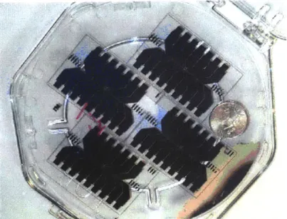
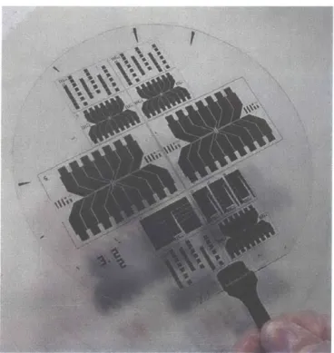
The first and second chip designs had a geometry consisting of two rows of resistive heating elements. In the first, the resistors were line resistors. In the second, the resistors were folded. Both designs used an out-of-plane etched cavity as the nucleation site. Each row of resistors in both generations spans a width of approximately 8 cm. Each resistive element could be utilized as a capture site. The upper layer silicon chip containing the etched bubble chamber and capture well was bonded to the quartz resistor chip shown in Figure 1-9. Each pair of platinum lines perpendicular to the long dimension of the chip represents the pair of leads for a resistive heating element. The pictured chip contains resistors of different geometries ranging in width from about 100 to 1000 gm. The package used to test the pBA application is shown in Figure 1-10. Assembled, the first-generation package was
Arrayed Microfluidic Actuation for Active Sorting of Fluid Bed Particulates
Figure 1-9. Early pBA Fabricated Chip.
Aluminum cap
Outlet 4--%.
Glass slide
PDMS gasket
Silicon particle manipulation chip Quartz resistor heater chip
PDMS gasket
. Aluminum block
- Inlet
-- Backflow
Figure 1-10. First-Generation Package [681.
1.3 Objective
In previous work [67-70, 83], the pBA technique was shown to be capable of
nucleating a thermally formed microbubble at a specified location and dissipating that bubble on a time scale of the order of seconds. Additionally, a proof-of-concept pBA-driven device was shown to be capable of capturing a particle at a predetermined location, holding the particle against the bulk flow, and releasing the particle at a chosen time. The next step in the development of the pBA technology is to use the information gained from characterizing
Chapter 1 Introduction
the microbubble formation properties and the first-generation piBA-driven device to design arrayed ptBA-driven actuation technology. This can be accomplished in conjunction with the goals of the pDAC project.
The main objective of this thesis is to demonstrate the feasibility of microbubble actuation as an arrayed particulate actuation technology for active sorting in particulate fluid beds. To accomplish this objective, (1) an arrayed pBA-driven device was designed and fabricated, (2) the pIBA technology was tested and characterized in detail including over a hundred in-plane and out-of-plane nucleation site geometries, and (3) technical guidelines for pBA-based devices and systems are presented. Therefore, in the course of research, the first-generation tBA for sorting technique was improved upon and further characterized while developing an application device that has the potential to serve as a tool for the researcher and scientist in the laboratory.
1.4 Scope
Chapter 1 provides an introductory background in the areas of microfluidics, pLBA, BioMEMS, and the pDAC project. In Chapter 2, some of the theory relevant to a ptBA-based device in industrial contexts is presented. Chapter 3 elucidates numerical and analytical models of flows, forces, and fields affecting a ptBA-based system. Chapter 4 describes fundamental parameters that influence design of a pBA device and the resulting device design for the pDAC application. Other applications of the pBA-powered technology that can be extrapolated from the pDAC design are discussed in the concluding sections. The focus of Chapter 5 is to discuss experimental hypotheses, protocols, and results of chip performance testing. The final chapter is dedicated to a discussion of the pBA chip performance including a detailed comparison of in-plane and out-of-plane nucleation site geometries, remaining problems and potential resolution for those problems, and suggestions for the focus of future work and potential pBA applications.
Arrayed Microfluidic Actuation for Active Sorting of Fluid Bed Particulates
1.5 References
[1] R. B. White and A. Zakhari, "Internal Structures in Fluid Beds of Different Scales: An Application of Electrical Capacitance Tomography," In Proc. 1st World Congress
on Industrial Process Tomography, Burdon, Greater Manchester, England, 1999, pp.
39-46.
[2] L. J. Shadle, E. R. Monazam, and J. S. Mei, "Circulating Fluid Bed Operating Regimes," In Proc. 7th International CFB Conference, Niagara Falls, New York, 2001, pp. 255-262.
[3] J. Tsai and L. Lin, "Transient Thermal Bubble Formation on Polysilicon
Micro-Resistors," Journal of Heat Transfer., vol. 124, Apr., pp. 375-3 82, 2002.
[4] A. Hatch, A. E. Kamholz, G. Holman, P. Yager, and K. F. B6hringer, "A Ferrofluidic
Magnetic Micropump," Journal ofMicroelectromechanical Systems, vol. 10, no. 2,
Jun., pp. 215-221, 2001.
[5] P. Dutta, A. Beskok, and T. C. Warburton, "Electroosmotic Flow Control in Complex Microgeometries," Journal ofMicroelectromechanical Systems, vol. 11, no. 1, Feb.,
pp. 36-44, 2002.
[6] S. Shoji and M. Esashi, "Microflow Devices and Systems," Journal of
Micromechanics and Microengineering, vol. 4, pp. 157-171, 1994.
[7] Y. Su, L. Lin, and A. P. Pisano, "A Water-Powered Osmotic Actuator," Journal of
Microelectromechanical Systems, vol. 11, no. 6, Dec., pp. 736-742, 2002.
[8] T. Stanczyk, B. Ilic, P. J. Hesketh, and J. G. B. IV, "A Microfabricated Electrochemical Actuator for Large Displacements," Journal of
Microelectromechanical Systems, vol. 9, no. 3, pp. 314-320, 2000.
[9] R. H. Liu,
Q.
Yu, and D. J. Beebe, "Fabrication and Characterization of Hydrogel -Based Microvalves," Journal of Microelectromechanical Systems, vol. 11, no. 1,Feb., pp. 45-53, 2002.
[10] A. K. Henning, "Microfluidic MEMS," In Proc. IEEE Aerospace Conference, vol. / paper 4.906, Piscataway, New Jersey: IEEE Press, 1998.
[11] H. Jerman, "Electrically-activated, normally closed diaphragm valves," Journal of
Chapter 1 Introduction
[12] H. Jerman, "Electrically-activated micromachined diaphragm valves," In Proc. IEEE
Solid State Sensors, Actuators, and Microsystems Workshop, Hilton Head, South
Carolina, 1990, pp. 65-69.
[13] J. S. Fitch, A. K. Henning, E. B. Arkilic, and J. M. Harris, "Pressure-based mass-flow control using thermopneumatically-actuated microvalves," In Proc. IEEE Solid-State
Sensor, Actuator, and Microsystems Workshop, Cleveland, Ohio: Transducers
Research Foundation, 1998, pp. 162-165.
[14] N. Vandelli, D. Wroblewski, M. Velonis, and T.Bifano, "Development of a MEMS
Microvalve Array for Fluid Flow Control," Journal of Microelectromechanical
Systems, vol. 7, no. 4, Dec., pp. 395-403, 1998.
[15] M. Koch, N. Harris, A. G. R. Evans, N. M. White, and A. Brunnschweiler, "A novel
micromachined pump based on thick-film piezoelectric actuation.," Sensors and
Actuators A: Physical, vol. 70, pp. 98-103, 1998.
[16] A. Manz, C. S. Effenhauser, N. Burggraf, D. J. Harrison, K. Seiler, and K. Fluri, "Electroosmotic pumping and electrophoretic separations for miniaturized chemical analysis systems," Journal ofMicromechanics and Microengineering, vol. 4, pp.
257-265, 1994.
[17] R. Zengerle, J. Ulrich, S. Kluge, M. Richter, and A. Richter, "A bidirectional silicon micropump," Sensors andActuators A: Physical, vol. 50, no. 1-2, pp. 81-86, 1995.
[18] R. Zengerle, M. Richter, F. Brosinger, A. Richter, and H. Sandmaier, "Performance simulation of microminiaturized membrane pumps," In Proc. 7th International
Conference of Solid-State Sensors, Actuators, and Microsystems (Transducers '93),
Yokohama, Japan, 1993, pp. 106-109.
[19] D. Armani and C. Liu, "Re-configurable Fluid Circuits By PDMS Elastomer
Micromachining," In Proc. 12th International Conference on MEMS (MEMS '99), Orlando, Florida, 1999, pp. 222-227.
[20] J. Voldman, M. L. Gray, and M. A. Schmidt, "An integrated liquid mixer/valve,"
Journal of Microelectromechanical Systems, vol. 9, pp. 295-302, 2000.
[21] J. Voldman, M. L. Gray, and M. A. Schmidt, "Liquid mixing studies using an
integrated mixer/valve," In Proc. Micro Total Analysis Systems (pTAS '98), Netherlands: Kluwer Academic Publishers, 1998, pp. 181-184.
Arrayed Microfluidic Actuation for Active Sorting of Fluid Bed Particulates
[22] M. Elwenspoek, T. S. J. Lammerink, R. Miyake, and J. H. J. Fluitman, "Towards integrated microliquid handling systems," Journal of Micromechanics and
Microengineering, vol. 4, pp. 227-245, 1994.
[23] D. C. Duffy, 0. J. A. Schueller, S. T. Brittain, and G. M. Whitesides, "Rapid
Prototyping of Microfluidic Switches in Poly(dimethyl siloxane) and their Actuation by Electro-osmotic Flow," Journal ofMicromechanics and Microengineering, vol. 9, no. 3, pp. 211-217, 1999.
[24] L. Latorre, J. Kim, J. Lee, P.-P. de Guzman, H. J. Lee, P. Nouet, and C.-J. Kim, "Electrostatic Actuation of Microscale Liquid-Metal Droplets," Journal of
Microelectromechanical Systems, vol. 11, no. 4, Aug., pp. 302-308, 2002.
[25] L. L. Chu, K. Takahata, P. Selvaganapathy, J. L. Shohet, and Y. B. Gianchandani, "A
Micromachined Kelvin Probe for Surface Potential Measurements in Microfluidic Channels and Solid-State Applications," In Proc. 12th International Conference on
Solid State Sensors, Actuators, and Microsystems (Transducers '03), vol. 1, Boston,
Massachusetts, 2003, pp. 384-387.
[26] J. Shih, J. Xie, and Y. C. Tai, "Surface Micromachined and Integrated Capacitive
Sensors for Microfluidic Applications," In Proc. 12th International Conference on
Solid State Sensors, Actuators, and Microsystems (Transducers '03), vol. 1, Boston,
Massachusetts, 2003, pp. 388-395.
[27] E. Meng and Y.-C. Tai, "A Parylene MEMS Flow Sensing Array," In Proc. 12th
International Conference on Solid State Sensors, Actuators, and Microsystems
(Transducers '03), vol. 1, Boston, United States, 2003, pp. 686-689.
[28] G. Hong, A. S. Holmes, M. E. Heaton, and K. R. Pullen, "Design, Fabrication, Characterization of an Axial-Flow Turbine for Flow Sensing," In Proc. 12th
International Conference on Solid State Sensors, Actuators, and Microsystems
(Transducers '03), vol. 1, Boston, Massachusetts, 2003, pp. 702-705.
[29] C.-J. Lin and F.-G. Tseng, "A Novel Micro Faby-Perot Sensor Utilizing Refractive Index Matched Medium for High Sensitive Shear Stress Sensing," In Proc. 12th
International Conference on Solid State Sensors, Actuators, and Microsystems
(Transducers '03), vol. 1, Boston, Massachusetts, 2003, pp. 710-713.
[30] F. Tseng, C. Kim, and C. Ho, "A High-Resolution High-Frequency Monolithic Top-Shooting Microinjector Free of Satellite Drops -Part I: Concept, Design, and Model,"
Chapter 1 Introduction
[31] F. Tseng, C. Kim, and C. Ho, "A High-Resolution High-Frequency Monolithic Top-Shooting Microinjector Free of Satellite Drops -Part II: Fabrication, Implementation, and Characterization," Journal of Microelectromechanical Systems, vol. 11, no. 5, pp. 437-447, 2002.
[32] S. S. Davis, "Biomedical applications of nanotechnology -implications for drug targeting and gene therapy," Trends in Biotechnology, vol. 15, Jun., pp. 217-224,
1997.
[33] Hewlett-Packard Company, "Myths About Thermal Inkjet Printings," [Online document], 1994, [cited 2003 July 21], Available HTTP: http://www.hp.com. [34] R. R. Allen, J. D. Meyer, and W. R. Knight, "Thermodynamics and Hydrodynamics
of Thermal Ink Jets," Hewlett-Packard Journal, vol. 36, May, pp. 21-27, 1985.
[35] B. Choi, M. Ma, C. White, and C. Liu, "Electrolytic and thermal bubble generation
using AC inductive powering," In Proc. 10th International Conference of Solid-State
Sensors, Actuators, and Microsystems (Transducers '99), Sendai, Japan, 1999.
[36] Agilent Technologies, "Building Australian businesses based on frontier
technologies," [Online document], 2003, [cited 2003 October 26], Available HTTP: http://www.agilent.com.
[37] Agilent Technologies, "Tiny bubbles -the secret to tomorrow's broadband networks," [Online document], 2000, [cited 2003 October 26], Available HTTP:
http://www.agilent.com.
[38] A. Asai, "Application of the Nucleation Theory to the Design of Bubble Jet Printers,"
Japanese Journal ofApplied Physics, vol. 28, pp. 909-915, 1989.
[39] C. C. Beatty, "A chronology of thermal ink-jet structures," In Proc. IEEE Solid-State
Sensor, Actuator, and Microsystems Workshop, Hilton Head, South Carolina, 1996,
pp. 200-204.
[40] R. Cole, "Boiling Nucleation," in Advances in Heat Transfer, J. P. Hartnett and T. F. Irvine, Eds. Chicago, Illinois: Academic Press, 1974.
[41] R. Cole and S. V. Stralen., Boiling Phenomena. vol. 1, Washington, D.C.: Hemisphere Publishing Corporation, 1979.
Arrayed Microfluidic Actuation for Active Sorting of Fluid Bed Particulates
[42] J. D. Evans and D. Liepmann, "The Bubble Spring and Channel (BSaC) Valve: An Actuated, Bi-stable Mechanical Valve for In-Plane Fluid Control," In Proc. 10th
International Conference on Solid-State Sensors, Actuators, and Microsystems
(Transducers '99), Sendai, Japan, 1999, pp. 1122-1125.
[43] X. Geng, H. Yuan, H. N. Oguz, and A. Prosperetti, "Bubble-Based Micropump for
Electrically Conducting Liquids," Journal of Micromechanics and Microengineering, vol. 11, no. 3, pp. 270-276, 2001.
[44] L. Lin and A. P. Pisano, "Bubble Forming on a Micro Line Heater," In Proc. DSC
ASME Micromechanical Sensors, Actuators, and Systems - Winter Annual Meeting,
vol. 32, 1991, pp. 147-163.
[45] L. Lin and A. P. Pisano, "Thermal Bubble Powered Microactuators," Microsystem
Technologies Journal, vol. 1, no. 1, pp. 51-58, 1994.
[46] L. Lin, A. P. Pisano, and A. P. Lee, "Microbubble Powered Actuator," In Proc. 6th
International Conference on Solid-State Sensors, Actuators, and Microsystems (Transducers '91), San Francisco, California, 1991, pp. 1041-1044.
[47] L. Lin, K. S. Udell, and A. P. Pisano, "Phase Change Phenomena on a Heated Polysilicon Micro Heater in Confined and Unconfined Micro Channels," Thermal
Sciences and Engineering, vol. 2, pp. 52-59, 1994.
[48] L. S. Tong and Y. S. Tang, Boiling Heat Transfer and Two-Phase Flow. 2nd ed., Washington, D.C.: Taylor and Francis, Incorporated, 1997.
[49] J. Tsai and L. Lin, "A Thermal-Bubble-Actuated Micronozzle-Diffuser Pump,"
Journal ofMicroelectromechanical Systems, vol. 11, no. 6, Dec., pp. 665-671, 2002. [50] J. Tsai and L. Lin, "Nozzle-Diffuser Based Micro Bubble Pump," In Proc. Late News
Poster Session Supplemental Digest of IEEE Solid-State Sensors, Actuators, and Microsystems Workshop, Hilton Head, South Carolina, 2000, pp. 13-14.
[51] J. Tsai and L. Lin, "Transient Bubble Formation On A Polysilicon Micro Resister," In
Proc. 2000 ASME International Mechanical Engineering Congress and Exposition, ASME Heat Transfer Division, vol. 2, Orlando, Florida, 2000, pp. 251-258.
[52] J. Tsai and L. Lin, "Active Microfluidic Mixer and Gas Bubble Filter Driven by Thermal Bubble Micropump," Sensors and Actuators A: Physical, vol. 97-98, pp. 665-671, 2002.