Publisher’s version / Version de l'éditeur:
OPTICS LETTERS, 35, 19, pp. 3243-3245, 2010-10-01
READ THESE TERMS AND CONDITIONS CAREFULLY BEFORE USING THIS WEBSITE. https://nrc-publications.canada.ca/eng/copyright
Vous avez des questions? Nous pouvons vous aider. Pour communiquer directement avec un auteur, consultez la
première page de la revue dans laquelle son article a été publié afin de trouver ses coordonnées. Si vous n’arrivez pas à les repérer, communiquez avec nous à [email protected].
Questions? Contact the NRC Publications Archive team at
[email protected]. If you wish to email the authors directly, please see the first page of the publication for their contact information.
NRC Publications Archive
Archives des publications du CNRC
This publication could be one of several versions: author’s original, accepted manuscript or the publisher’s version. / La version de cette publication peut être l’une des suivantes : la version prépublication de l’auteur, la version acceptée du manuscrit ou la version de l’éditeur.
For the publisher’s version, please access the DOI link below./ Pour consulter la version de l’éditeur, utilisez le lien DOI ci-dessous.
https://doi.org/10.1364/OL.35.003243
Access and use of this website and the material on it are subject to the Terms and Conditions set forth at
Continuously apodized fiber-to-chip surface grating coupler with
refractive index engineered subwavelength structure
Halir, R.; Cheben, P.; Schmid, J. H.; Ma, R.; Bedard, D.; Janz, S.; Xu, D.-X.;
Densmore, A.; Lapointe, J.; Molina-Fernández, Í.
https://publications-cnrc.canada.ca/fra/droits
L’accès à ce site Web et l’utilisation de son contenu sont assujettis aux conditions présentées dans le site LISEZ CES CONDITIONS ATTENTIVEMENT AVANT D’UTILISER CE SITE WEB.
NRC Publications Record / Notice d'Archives des publications de CNRC:
https://nrc-publications.canada.ca/eng/view/object/?id=a5dad129-0899-463a-9c49-5e686f2cfe8e https://publications-cnrc.canada.ca/fra/voir/objet/?id=a5dad129-0899-463a-9c49-5e686f2cfe8e
Continuously apodized fiber-to-chip surface
grating coupler with refractive
index engineered subwavelength structure
R. Halir,1,* P. Cheben,2,3J. H. Schmid,2 R. Ma,2D. Bedard,2S. Janz,2D.-X. Xu,2A. Densmore,2
J. Lapointe,2and Í. Molina-Fernández1
1Departamento Ingeniería de Comunicaciones, ETSI Telecomunicación, Universidad de Málaga, 29010 Málaga, Spain
2Institute for Microstructural Sciences, National Research Council of Canada, Ottawa, Ontario, K1A 0R6, Canada 3e-mail: [email protected]
*Corresponding author: [email protected] Received July 30, 2010; accepted August 27, 2010;
posted September 9, 2010 (Doc. ID 132100); published September 23, 2010
We demonstrate a fully etched, continuously apodized fiber-to-chip surface grating coupler for the first time (to our knowledge). The device is fabricated in a single-etch step and operates with TM-polarized light, achieving a cou-pling efficiency of 3:7 dB and a 3 dB bandwidth of 60 nm. A subwavelength microstructure is employed to generate an effective medium engineered to vary the strength of the grating and thereby maximize coupling efficiency, while mitigating backreflections at the same time. Minimum feature size is 100 nm for compatibility with deep-UV 193 nm lithography. © 2010 Optical Society of America
OCIS codes: 130.0130, 050.2770, 050.6624.
Owing to their compact size and tight light confinement, silicon-wire waveguides provide a very attractive plat-form for the integration and miniaturization of photonic devices [1], such as wavelength demultiplexers [2,3], fil-ters [4], and evanescent field sensors [5,6], to cite but a few. While the former are often operated with TE polar-ization, the latter exploit the strong evanescent field of the TM polarization state to maximize sensitivity. In either case, efficient coupling of light from an optical fi-ber to (and from) the microphotonic chip is challenging because of the small size of the silicon waveguide core (∼250 nm × 450 nm). Surface grating couplers are a pro-mising fiber–chip coupling solution [7,8]. They operate by laterally expanding the light propagating in the wave-guide by means of an adiabatic taper, along with diffrac-tion coupling it to (or from) an optical fiber posidiffrac-tioned over the grating [see Fig.1(a)]. To achieve good coupling efficiency, the grating must exhibit a high directionality toward the fiber, and the radiated field should match the near-Gaussian field of the optical fiber mode. It appears that directionalities well above 60% can be achieved only with specialized layer structures [8–10] that, however, re-quire a complex fabrication sequence to implement. To control their strength, gratings are usually defined in a second, shallow etch depth [8]. For full optimization of the field overlap, the grating has to apodized, and, to this end, use of the etch lag effect in the shallow etch has been recently shown [11]. However, the ideal fabrication process would use a single full etch through the silicon to the buried oxide (BOX) to define both the waveguides and the grating couplers.
In [12], we proposed, for the first time (to our knowl-edge), the use of a grating formed by alternating effective medium regions with regions of unpatterned silicon, as in Fig.1(a). The effective medium is created by fully etched structures with feature size and periodicity smaller than the operating wavelength. This enables single-etch fabrication of gratings with the appropriate strength and simultaneous apodization to optimally match the
ra-diated field to the fiber mode. Simulations predict that an improvement of up to 1:2 dB in coupling efficiency and substantial reduction in backreflections can be achieved with apodized designs.
Two implementations of this concept have appeared so far in literature [13,14], using circular nanoholes to create the effective medium. However, both designs are uniform (nonapodized) and operate with TE-polarized light.
Building upon our previous theoretical study [12], here we experimentally demonstrate a continuously apodized, fully etched grating coupler. Furthermore, the design operates for TM polarization and has feature sizes com-patible with deep-UV (DUV) lithography. This work
Fig. 1. (Color online) (a) Schematic drawing of the fiber-to-waveguide coupling scheme using a grating coupler. (b) Scanning electron microscope image of the fabricated coupler. (c) Enlargement of the boxed area in (b).
October 1, 2010 / Vol. 35, No. 19 / OPTICS LETTERS 3243
complements our recent experimental demonstrations of refractive index engineering using subwavelength nano-structures in fiber–chip edge couplers and optical multi-plexers [15].
A continuously apodized grating coupler was designed and fabricated using a 0.26-μm-thick silicon layer with a 2-μm-thick BOX and air cladding. An unapodized design was also included as a reference. As detailed in [12], the design of the grating is based upon two two-dimensional (2D) models. First, the subwavelength structure is mod-eled as a multilayer slab waveguide in the xz plane. The effective index of the fundamental mode of this slab gives the equivalent medium index, which can be tuned by varying its duty cycle in a wide range of 3.22 to 2.16 for a minimum feature size of 100 nm. Second, the equivalent medium index is used in a 2D model of the grating coupler in the yz plane. Using 2D finite-difference time-domain (FDTD) simulations, the grating is then op-timized to produce maximum coupling to the fiber situ-ated above the grating. In [12], we verified this design approach with three-dimensional (3D) FDTD simula-tions, and the results presented in this Letter confirm the validity of this approach experimentally.
The pitch of the subwavelength structure was set to Λx¼ 450 nm, which yields a minimum feature size of 100nm compatible with 193 nm DUV lithography. We verified with 3D FDTD simulations that this pitch still ef-fectively suppresses diffraction effects in the lateral (x) direction.
For the reference (unapodized) grating, the equivalent medium is required to have an effective index of 2.73, which is achieved with a duty cycle of 59% in the sub-wavelength structure. This yields a minimum feature 184nm, which can be readily fabricated with DUV litho-graphy. In the longitudinal (z) direction, the pitch was ad-justed to Λz¼ 0:84 μm to produce a radiation angle of ∼12° with respect to the grating normal. The duty cycle in the z direction is 70% silicon to effective medium, and the coupler consists of 17 periods arrayed along the longitudinal (z) direction, comprising alternating lines of silicon and the subwavelength structures Fig.1(b). As shown in Fig.2, simulations predict a maximum coupling efficiency of 4 dB for this design, with a 3 dB bandwidth of ∼60 nm (∼35 nm at 1 dB) and a backreflection of ∼1%.
Unlike in the reference grating, in our continuously apodized coupler, the equivalent medium index was var-ied linearly from 3.22 to 2.16 from the grating junction with the lateral taper to the end of the grating. These ef-fective indices apodize the strength of the grating to pro-duce a near-Gaussian radiated field (see inset of Fig.2). The minimum feature size required to synthesize these equivalent medium indices with a Λx¼ 450 nm subwave-length grating pitch is 100 nm, for compatibility with DUV lithography. The pitch in the longitudinal (z) direc-tion was varied along the grating, so that all grating periods contribute light to the radiated beam with the correct phase [11,12]. The total length of the coupler is 20μm, and a 50% duty cycle is used in the z direction. As shown in Fig. 2, coupling efficiency is improved to ∼2:8 dB, with a 3 dB bandwidth of 64 nm (∼35 nm at 1dB). Furthermore, since the change in refractive index between the waveguide and the grating coupler is re-duced, backreflections are reduced tenfold down to ∼0:1%.
For testing, identical grating couplers were arranged in a back-to-back configuration so as to couple light from the fiber into the waveguide with one of them and extracting it with the other. In fabrication, the grating couplers and waveguides were defined in a single patterning step by
Fig. 2. (Color online) Simulated coupling efficiency as a func-tion of wavelength for the unapodized and the apodized design. The inset compares the fiber mode with the field radiated by the unapodized and apodized grating.
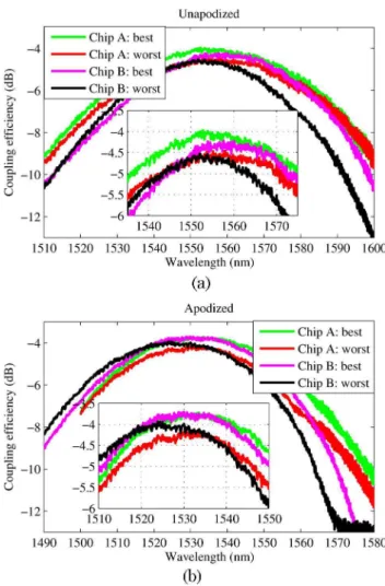
Fig. 3. (Color online) Measured coupling efficiency of (a) the unapodized grating coupler and (b) the apodized grating cou-pler. The best and worst gratings from two chips are shown, indicating a good repeatability.
electron-beam lithography with a high-contrast hydrogen silsesquioxane resist, which forms SiO2 upon
electron-beam exposure. Inductively coupled plasma reactive ion etching was used to transfer the resist pattern into the silicon layer. Scanning electron microscope images of the fabricated structure are shown in Figs. 1(b) and
1(c), indicating a very good definition of the square holes. The measurement of the grating couplers was carried out by positioning fibers above them and recording the insertion loss as a function of wavelength. The coupling efficiency was determined from the insertion loss of two back-to-back connected couplers, subtracting the loss of the Si-wire interconnecting waveguide. The length of these waveguides was 3:7 mm, with measured losses of 3:2 dB=cm. The slight reflections from the fiber facets introduce a Fabry–Perot ripple of0:1 dB in the transmis-sion spectrum, which means that backreflections from the gratings smaller than 0.8% cannot be detected.
The experimental results for the uniform and the apo-dized gratings are shown in Fig.3. The best uniform grat-ing achieves a couplgrat-ing efficiency of 4 dB [see Fig.3(a)], which is in excellent agreement with simulations. A series of gratings from two different chips were tested, the worst showing a coupling efficiency of 4:5 dB, which indicates a good repeatability of the structure. From the small (0:2 dB) Fabry–Perot ripple in the coupling spectrum [(see inset in Fig.3(a)], the grating reflectivity was estimated to be ∼1:5%. The 3 dB bandwidth of the grating is 65 nm (40 nm at 1 dB). As shown in Fig.3(b), the apodized grating shows a peak coupling efficiency of ∼3:7 dB. This is an ∼0:3 dB improvement with respect to the unapodized design, which is, however, smaller than predicted by simulation. This is attributed to variations in the fabrication process, because the duty cycle and the pitch of each individual period have to be matched pre-cisely for all the grating elements to contribute to the total light beam with the proper phase. The worst grating exhi-bits a coupling efficiency of 4:3 dB, also indicating good reproducibility. The Fabry–Perot ripple is improved with respect to the uniform grating to below 0:15 dB. This cor-responds to a reflectivity below 1%, most of which is at-tributed to the fiber facets. The 3 dB bandwidth of the apodized grating is 60 nm (38 nm at 1 dB).
We have demonstrated a first continuously apodized ef-fective medium based fiber–chip grating surface coupler for TM polarization. Using a comparatively simple layer structure and a single etch step, a coupling efficiency of 3:7 dB is achieved with a 3 dB bandwidth of 60 nm. The coupler has a minimum feature size of 100 nm
(184 nm for the unapodized design) and can thus be fabricated with DUV lithography. While the concepts of effective material engineering shown here are of wide ap-plicability, these results are of particular importance for evanescent field biosensing applications, which require efficient and robust couplers for TM polarization, where sensitivity is maximized [5,6].
This work has been supported by the National Re-search Council of Canada (NRC) Genomics and Health Initiative, the Spanish Ministerio de Ciencia e Innovación under project TEC2009-10152, a FPU scholarship AP-2006-03355, and by the Andalusian Regional Ministry of Science, Innovation and Business under project TIC-02946.
References
1. R. Soref, IEEE J. Sel. Top. Quantum Electron. 12, 1678 (2006).
2. P. Cheben, J. Schmid, A. Delâge, A. Densmore, S. Janz, B. Lamontagne, J. Lapointe, E. Post, P. Waldron, and D.-X. Xu, Opt. Express 15, 2299 (2007).
3. P. Bock, P. Cheben, A. Delâge, J. H. Schmid, D.-X. Xu, S. Janz, and T. J. Hall, Opt. Express 16, 17616 (2008). 4. F. Horst, in Optical Fiber Communication Conference
(Optical Society of America, 2010).
5. A. Densmore, D.-X. Xu, P. Waldron, S. Janz, P. Cheben, J. Lapointe, A. Delâge, B. Lamontagne, J. Schmid, and E. Post, J. Lightwave Technol. 18, 2520 (2006).
6. D.-X. Xu, A. Densmore, A. Delâge, P. Waldron, R. McKinnon, S. Janz, J. Lapointe, G. Lopinski, T. Mischki, E. Post, P. Cheben, and J. H. Schmid, Opt. Express 16, 15137 (2008).
7. T. Tamir and S. Peng, Appl. Phys. 14, 235 (1977). 8. D. Taillaert, P. Bienstman, and R. Baets, Opt. Lett. 29,
2749 (2004).
9. P. Cheben, S. Janz, D.-X. Xu, B. Lamontagne, A. Delâge, and S. Tanev, IEEE Photonics Technol. Lett. 18, 13 (2006).
10. G. Roelkens, D. Vermeulen, D. Van Thourhout, R. Baets, S. Brision, P. Lyan, P. Gautier, and J. Fédéli, Appl. Phys. Lett. 92, 131101 (2008).
11. Y. Tang, Z. Wang, L. Wosinski, U. Westergren, and S. He, Opt. Lett. 35, 1290 (2010).
12. R. Halir, P. Cheben, S. Janz, D.-X. Xu, Í. Molina-Fernández, and J. G. Wangüemert-Pérez, Opt. Lett. 34, 1408 (2009). 13. X. Chen and H. Tsang, IEEE Photonics J. 1, 184 (2009). 14. L. Liu, M. Pu, K. Yvind, and J. Hvam, Appl. Phys. Lett. 96,
051126 (2010).
15. P. Cheben, P. J. Bock, J. H. Schmid, J. Lapointe, S. Janz, D.-X. Xu, A. Densmore, A. Delâge, B. Lamontagne, and T. J. Hall, Opt. Lett. 35, 2526 (2010).