HAL Id: hal-01205295
https://hal.archives-ouvertes.fr/hal-01205295
Submitted on 25 Sep 2015
HAL is a multi-disciplinary open access
archive for the deposit and dissemination of
sci-entific research documents, whether they are
pub-lished or not. The documents may come from
teaching and research institutions in France or
abroad, or from public or private research centers.
L’archive ouverte pluridisciplinaire HAL, est
destinée au dépôt et à la diffusion de documents
scientifiques de niveau recherche, publiés ou non,
émanant des établissements d’enseignement et de
recherche français ou étrangers, des laboratoires
publics ou privés.
Integrated waveguide interferometer with picometric
performances
Alexia Missoffe, Serge Olivier, Barthélemy Cagneau, Pierre Millier, Hongyu
Guan, Luc Chassagne
To cite this version:
Alexia Missoffe, Serge Olivier, Barthélemy Cagneau, Pierre Millier, Hongyu Guan, et al.. Integrated
waveguide interferometer with picometric performances.
AIM 2014 - IEEE/ASME International
Conference on Advanced Intelligent Mechatronic, Jul 2014, Besançon, France. pp.1134-1138.
�hal-01205295�
Integrated waveguide interferometer with picometric performances
A. Missoffe, S. Olivier, B. Cagneau, P. Millier, H. Guan, L. Chassagne
Abstract— We present an integrated optical waveguide interferometer highly compact and easy-to-use. Metrological study is focused on the resolution and the noise level of the sensor. A standard Allan deviation lower than 50 pm has been observed in standard environment. Power spectral densities up to 150 fm.Hz-1/2 at 10 kHz are achieved. The flicker level is not reached because of the environmental conditions but the high frequency noise is likely to be lower than 100 fm. Hz-1/2. We present measures for steps of 0.5 nm at a sample frequency of 1 kHz. Although we use it as sensing motions measurement over micrometric range, the maximum displacement range is 5 centimeters depending on the output lens which is used.
I. INTRODUCTION
Micro- and nanotechnology fields ask for the development of tools and apparatus dedicated to the micro- and nanoscales. Several applications highly depend on the quality of the sensors either in laboratories or industry. Nowadays, the measurement of the position and the orientation are obviously a main topic for nanometrology. It may concern the positioning of nano-object to manipulate them [1] but also the positioning of macro-object like sample-holder or macro-tools. Resolutions up to the nanometer or tens of picometers are now achieved thanks to the sensors which have been developed. In this paper, we are interested in sensors with sub-nanometer accuracy over a range of several centimeters. This kind of sensors is quite difficult to develop since these performances are usually not compatible with high bandwidth, sensitivity to refractive index, compactness and costs.
The interferometry is obviously a good solution that combines both accuracy and long range measurement. Moreover, interferometers allow for accurate and traceability for displacement measurements. Nevertheless, their sensitivity to the medium index and their price make difficult to use in many applications. Encoders are the main rivals of interferometers. Invar or zerodur gratings can be produced over long range with sub-micrometric periods. Encoders with high performances ensure nanometric resolution over centimetric ranges with high repeatability and very low periodic non-linearities [2]. However, it is to the detriment of the price and the compactness. Fabry-Perot interferometers can present high ratio range over resolution
B. Cagneau, H. Guan and L. Chassagne are with the Université de Versailles St-Quentin en Yvelines / LISV, 10-12 Avenue de l’Europe, 78140, France (e-mail: [email protected]).
A. Missofffe was with UVSQ / LISV and is now with IADI-INSERM, Université de Lorraine, 54511 Vandoeuvre-lès-Nancy, France.
S. Olivier and P. Millier are with CEA/DAM/DIF/DASE, Bruyères-le-Chatel, 91297 Arpajon CEDEX, France
but remain highly sensitive to the tuning for fibre models or very complexes [3]. For cheaper sensors, the inductive ones achieve good resolution but low accuracy. Capacitive sensors are a good compromise but long range is difficult to perform and the bandwidth remains around a few kilohertz. Integrated systems with coupling fiber systems have also been hardly developed with a very low price. Nanometric performances can be reached with an emitting fiber coupled with collecting fibers. High resolution or high bandwidth [4-7] are possible but with limited range and low accuracy because of long-term drifts. Others triangulation systems with CCD or photodiodes array elements have been developed but the compactness and the bandwidth are still limited [8].
The main drawbacks of interferometers remain the price, the compactness and the sensitivity to refractive index. Nevertheless, the development of a highly integrated interferometer with easy-to-use capabilities remains a challenge for several applications in nanotechnology. This is especially true for unskilled users who need to set up the optical path. For example, the use of fully integrated interferometers is not so easy in microscopy. The main reasons are because of the compactness and the detection of the cantilever motions. Nowadays, the measurements are mostly performed with optical beam deflection which can exhibit high performances for high frequencies [9].
This paper presents an optical chip based on interferometry, high compactness and low sensitivity to refractive index. It is inspired of telecom systems and is composed of an optical chip with optical waveguides. Its simplicity of use combined with high performances made the system very promising. We plan to use this sensor with a nano-displacement platform for nano-manipulation and for a sample-holder in microscopy or lithography process [10-11].
II. INTERFEROMETRY SETUP
The interferometer has been first designed for geophysical applications by the CEA1. Its purpose was to obtain a very low noise level and a high dynamic, especially for low frequencies. The first setup has been described in [12] where a first prototype has been built and evaluated. This prototype, made with macroscopic optical components, demonstrates very good results as low as 100 fm.Hz-1/2 at 8 Hz. The second version has been built with integrated waveguide technology to enhance the robustness to environmental disturbances.
1
CEA is a french acronym for “Commissariat à l’énergie atomique”
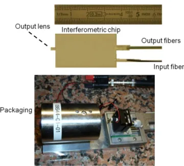
It is fully integrated in an optical chip with an optical waveguide structure. Technology used for the chip is described by Malbet et al [13]. The chip has been made by Teem Photonics, company known for their knowledge of integrated optics process developed in telecom fields. The chip is illustrated in Fig. 1a. All the input and the output are fibered. One can see that the chip is very small and compact; the thickness is only a few millimeters. The chip is inserted in a package made of steel for vibration isolation and thermal homogeneity (Fig. 1b). Note that next version will perform a higher compactness in order to use it in highly integrated systems. The output lens focuses the beam toward a mobile mirror and makes the system very easy-to-use because there is no need for other lenses.
FIG. 1. Photography of the interferometer: a) Chip with an integrated waveguide; b) The interferometer inside its packaging and an external mobile mirror moved by a piezoelectric actuator. The interferometer integrated in the chip is a Michelson interferometer. The waveguides are designed for the 1.55 µm telecom window wavelength. Several couplers separate the beam for the two references arms and the two measurements arms (sine-cosine outputs). Details of the principle with free beams and optical components can be found in [12]. At the output, a collimating Grin lens ensures a useful range of several centimeters. Coming back from the mobile mirror, the light is re-injected in the chip. The four outputs are sent to photodetector modules to obtain voltages (transimpedance structures).
When interference patterns are recorded, the Eq. (1) describes the classical evolution of the patterns function of the displacement: 1 1 2 1 2
2
2
cos
mes
I
I
I I
, (1)where I1 and I2 are photometric parameters, λ is the
wavelength in the medium, and
the optical pathdifference. The equation for the output mes2 is similar to
Eq. (1) but with a sinusoidal function because of the phase shift of /2.
Once the ellipse is fully calibrated by the Lissajous estimation, the measurement of the output phase of the interferometer is derived from both Eq. (1) and the similar equation for mes2. The contrast can be enhanced by
suppressing the offsets with the two reference signals; it enhances the signal to noise ratio by suppressing the amplitude noise of the laser source or amplitude fluctuations due to the retro-injection perturbations caused by vibrations. By the way, the interference fringes are easily obtained with the Lissajous curve estimation [12] and finally, the output expression of the displacement is a classical one:
. 4 x , (2)
where is the phase variation measured by the Lissajous method and
x
the displacement of the mobile mirror. The computation of the ellipse is made in real-time and the bandwidth of the output of the interferometer is actually limited by the sample frequency of the data acquisition board.The only limitation on the computing is on the maximum displacement speed. The maximum phase shift between two acquisitions is 3/2 for indetermination reasons. For a sample frequency of 20 kHz and a wavelength of 1.55 µm, the maximum speed is almost 1.2 cm.s-1 and is sufficient for many applications in nano or microtechnologies.
III. EXPERIMENTAL SETUP
The four signals are sampled with an analog to digital board (NI PCI-4472) which is a very low noise sample system dedicated to noise sound analysis. The highest sample frequency is 45 kHz allowing 24 full bits resolution. The four signals are acquired with a homemade Labview software developed by the CEA. It includes low-pass filtering, statistical analysis and calculus of the ellipse. The position is then computed and recorded in data files for post-treatment analysis. Sample frequency and parameters of the filters are programmable.
The laser source is a telecom laser module (ORION Rio0085-1-00-1) with a wavelength value of 1542.135 nm. The uncertainty and the influence of the wavelength will be discussed in the sequel. The source is connected to the interferometer module with an optical fiber and the power can be modified.
The external mobile mirror used for the tests is a simple mirror mounted on tilt mechanical stages for tuning. The mechanical stage can be moved by a piezoelectric actuator along the axis of the measurement. Some experiments have been also done with a microscope objective (×4 or ×10) in order to check that focusing is possible without changing performances, which can be useful in some applications. The experimental setup is placed on a passive heavy table of granite (1500 kg) to cut-off building vibrations. The
interferometer and the mobile mirror are in a box for temperature regulation and a special isolating material (barson, mainly made of rubber and lead) to prevent external sound perturbations. There is no active temperature regulation but it can be recorded if necessary.
IV. RESULTS AND DISCUSSIONS
A. Experimental results
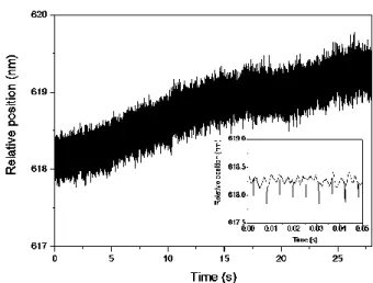
The interferometer is coupled with a mobile mirror. Once the returned signal is optimized, measurements are recorded for a static position of the mirror. The distance between the output collimating lens and the mirror can be adjusted. In nominal conditions, it is around 20 mm, but several sets of distance have been tested (up to 50 mm) and results are very similar. Fig. 2 illustrates direct measurements with respect to the time. Sample frequency is nominally chosen to 20 kHz. A drift of 1 nm appears, due to perturbation on the environmental conditions. The insert is a zoom showing also a residual mechanical oscillation, due to the mechanical stage supporting the mirror (amplitude ~ 200 pm, frequency ~ 200 Hz). The resolution is estimated taking into account the noise standard deviation, once drift and oscillation are compensated. For a precise estimation of the standard deviation, several sets of measurements have been recorded, either over short time with 20 kHz sample frequency, or with mid and long term range with 100 Hz sample frequency. For mid and long term measurements, drifts have been compensated. Allan standard deviation [14] y has
been estimated for different integration time . Note that the slight residual oscillation has not been compensated because it would have required band-pass filtering and we considered that it could have suppressed useful information. Results are presented in Fig. 3 for integration times between 50 µs and 680 s. The slight bump between 10-3 and 10-1 s is probably due to the residual mechanical free oscillation. The drift for long term estimation is due to residual environment perturbations. Nevertheless, one can see that the standard deviation is lower than 100 pm for all the range of measurement. It is likely that with better environmental conditions (vacuum condition or air conditioning, active anti-vibration table and no residual mechanical oscillation) the performances could approach 10 pm level (as seen with estimation of y for > 10-1 s with the 20 kHz sample
frequency set).
FIG. 2. Measurements of the relative position of the mirror in static configuration (20 kHz sample frequency). The drift is due to residual environmental perturbations. The insert is a zoom showing a residual mechanical oscillation of the stages (200 pm - 200 Hz).
FIG. 3. Allan standard deviation of measurements in a static configuration of the mobile mirror. The short and mid term estimations show performances below 100 pm. Long term estimations depend on drifts due to environmental perturbations and are not related to the sensors performances.
Fig. 4 corresponds to the power spectral density (sample frequency 20 kHz). The data acquisition board is limited and high frequency cannot be thus measured. However, we can estimate values of 600 fm.Hz-1/2 @1 kHz and 150 fm.Hz-1/2 @10 kHz. The flicker level is not reached but the high frequency noise is likely to be lower than 100 fm.Hz-1/2. In comparison to the state of the art, for a very easy to use apparatus, the performances are very good. As said previously, the performances measured are also limited by the test conditions but the intrinsic level is probably better.
FIG.4 Power spectral density (PSD) of the vibration measurements on the mirror in a static configuration. The estimated noise is 600 fm.Hz-1/2 @1 kHz and 150 fm.Hz-1/2 @10 kHz. The flicker noise is not reached at 10 kHz but the data acquisition board is limited for higher sample frequencies.
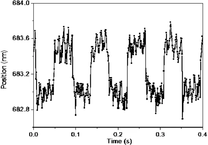
Fig. 5 shows dynamic measurements. The piezoelectric is fed by a low frequency square signal (11 Hz) of 3 mV peak-to-peak amplitude. We can clearly see 450 pm steps (the sample frequency is equal to 1 kHz). However, the piezoelectric actuator is in an open-loop configuration so that the steps are very disturbed. One can also notice that the residual mechanical oscillation appears because of the resolution and the noise of the measurements apparatus which are lower than 100 pm.
FIG. 5 Steps of 0.5 nm (sample frequency 1 kHz). The piezoelectric is in an open-loop configuration and one can see that the measurement resolution of the interferometer is below 0.1 nm; one can see also a residual mechanical oscillation around 0.15 nm amplitude.
In a third phase of the experiment, we focused the beam with a microscope objective (×4 or ×10) on a mobile mirror. The Allan standard deviation of the results is illustrated in Fig. 6. One can see that 10 pm noise level is achieved. The improvement is due to the collecting surface of the objective that enhances the collection of the beam at the output of the
interferometer; the signal to noise ratio is then higher and the stability improved.
FIG. 6 Allan standard deviation in a static configuration of the mobile mirror.
B. Discussion
The measurements show very good results over noise limitations. With respect to the state of the art, this system exhibits the performances of commercial systems as far as noise level is concerned. Let us emphasize that to be fully rational, the noise level must be compared for the same frequencies. The bandwidth of our first experimental setup is limited by the sample frequency of the data acquisition board, but the PSD show no flicker noise at 10 kHz. The noise is probably lower at higher frequencies. Furthermore, environmental conditions are not ideal. The residual vibrations and the temperature unstabilities are still limiting the results. In seismometer previous experiments, the first setup was tested in a seismic station (the quietest French station belonging to a national network with a deep cave very well isolated) and the results show 100 fm.Hz-1/2 @8 Hz. But such conditions are not possible in our laboratory. For temperature change, 100 pm level is around 0.01 K change on the refractive index of air in our setup, which is hardly the case for mid or long term measurements. For long term measurements, the influence of the source is also a criterion. Relative standard Allan deviation of the source is limited to 10-8 (i.e. 15 fm@1,55 µm) over thousand of seconds. Fluctuations are also directly correlated to temperature changes [14]. The documentation specifies ± 0.5 pm fluctuations for ± 1 °C variations.
The actual source is also a limitation for the range of the displacement. With a 1 °C uncertainty on the temperature conditions, the relative uncertainty on the wavelength is almost 3.10-7. The maximum displacement range if accuracy is important is then equal to the resolution divided by 3.10-7. For example, if an accuracy of 1 nm is required, the maximum possible range becomes around 3 mm. Although
for most applications concerning vibrations measurements this is mainly convenient, for other kind of applications like in multiscale imaging device, such a displacement range could be a limiting factor.
We plan to change the laser source for a red source. Firstly for convenience for the focusing on the cantilever, and secondly because it opens the door to highly stable sources as He-Ne laser for example. Nevertheless, it requires a new design of the chip to adapt the technology of the waveguides.
Another forthcoming evolution is the reduction of the dead path inside the reference arm. The seismologic tests have shown that the influence of the dead arm limits the vibration measurement at low frequency. We think that even for microscopy applications, it could be interesting to minimize this effect.
ACKNOWLEDGMENTS
This research was supported by the French research ministry (ANR-Pnano program) and CEA funding. Authors thank the Conseil Général des Yvelines, Frédéric Mourgues for mechanical support, and Florent Gardillou and Denis Barbier for fruitful discussions about the interferometer chip.
REFERENCES
[1] C. Pacoret, S. Régnier, A review of haptic optical tweezers for an interactive microworld exploration, Review of Scientific Instruments 84, 081301 (2013).
[2] A. Yacoot, N. Cross, Measurement of picometer non-linearity in an optical grating encoder using x-ray interferometry, Meas. Sci. Technol. 14 (2003) 148-152. [3] M. Durand, J. Lawall, Y. Wang, High-accuracy Fabry-Perot displacement interferometry using fiber lasers, Meas. Sci. Technol. 22 (2011) 094025.
[4] M. Yasin, S.W. Harun, K. Karyono, H. Ahmad, Fiber optic displacement sensor using a multimode bundle fiber, Microwave Opt.Technol. Letters 50 (2008) 661-663. [5] R. Dib, Y. Alayli, P. Wagstaff, A broadband amplitude-modulated fiber optic vibrometer with nanometric accuracy Measurement 35 (2004) 211-219.
[6] A. Khiat, F. Lamarque, C. Prelle, P. Phouille, M. Leester-Schädel, S. Büttganbach, Two-dimension fiber optic sensor for high-resolution and long-range linear measurements, Sens. Actuators A 158 (2010) 43-50.
[7] L. Perret, L. Chassagne, S. Topcu, P. Ruaux, B. Cagneau, Y. Alayli, Fiber optics sensor for sub-nanometric displacement and wide bandwidth systems, Sens. Actuators A, 165 (2011) 189-193.
[8] A. Missoffe, S. Topsu, P. Ruaux, B. Cagneau, Y. Alayli, New simple optical sensor: From nanometer resolution to centimeter displacement range, Sensors and Actuators A 176, 46– 52 (2012).
[9] C.A.J. Putman, B.G. de Grooth, N. F. van Hulst and J. Greve, A theoretical comparison between interferometric and optical beam deflection technique for the measurement of cantilever displacement in AFM, Ultramicroscopy 42-44, 1509-1513 (1992).
[10] L. Chassagne, S. Blaize, P. Ruaux, S. Topcu, P. Royer, Y. Alayli, G. Lérondel, Multi-scale Scanning probe Microscopy, Rev. Sci. Instrum., 81 (2010) 086101.
[11] G. Lérondel, A. Sinno, L. Chassagne, S. Blaize, P. Ruaux, A. Bruyant, S. Topçu, P. Royer, A. Alayli, Enlarged near-field optical imaging, J. Appl. Phys. 106 (2009) 044913.
[12] D. Ponceau, P. Millier and S. Olivier, Subnanometric Michelson interferometry for seismological applications, Proc. SPIE 7003 (2008).
[13] F. Malbet, P. Kern, I. Schanen-Duport, J.-P. Berger, K. Rousselet-Perraut, and P. Benech, Integrated Optics for Astronomical Interferometry, Astron. Astrophys. Suppl. Series 138 (1999).
[14]D. W. Allan, H. Hellwig, and D. J. Glaze, An Accuracy Algorithm for an Atomic Time Scale, Metrologia 11, 133 (1975).