HAL Id: hal-02548633
https://hal.archives-ouvertes.fr/hal-02548633
Submitted on 16 Nov 2020
HAL is a multi-disciplinary open access
archive for the deposit and dissemination of
sci-entific research documents, whether they are
pub-lished or not. The documents may come from
teaching and research institutions in France or
abroad, or from public or private research centers.
L’archive ouverte pluridisciplinaire HAL, est
destinée au dépôt et à la diffusion de documents
scientifiques de niveau recherche, publiés ou non,
émanant des établissements d’enseignement et de
recherche français ou étrangers, des laboratoires
publics ou privés.
Observation of Large Unidirectional Rashba
Magnetoresistance in Ge(111)
T. Guillet, C. Zucchetti, Q. Barbedienne, Marty A., G. Isella, L. Cagnon, C.
Vergnaud, H. Jaffrès, N. Reyren, J.-M. George, et al.
To cite this version:
T. Guillet, C. Zucchetti, Q. Barbedienne, Marty A., G. Isella, et al.. Observation of Large
Unidirec-tional Rashba Magnetoresistance in Ge(111). Physical Review Letters, American Physical Society,
2020, 124 (2), pp.027201. �10.1103/PhysRevLett.124.027201�. �hal-02548633�
T. Guillet,1 C. Zucchetti,2 Q. Barbedienne,3 A. Marty,1 G. Isella,2 L. Cagnon,4
C. Vergnaud,1 N. Reyren,3 J.-M. George,3 A. Fert,3 and M. Jamet1
1
Univ. Grenoble Alpes, CEA, CNRS, Grenoble INP, IRIG-SPINTEC, 38000 Grenoble, France
2LNESS-Dipartimento di Fisica, Politecnico di Milano,
Piazza Leonardo da Vinci 32, 20133 Milano, Italy
3
Unit´e Mixte de Physique, CNRS, Thales, Univ. Paris-Sud, Universit´e Paris-Saclay, 91767, Palaiseau, France
4Univ. Grenoble Alpes, CNRS, Grenoble INP, Institut NEEL, 38000 Grenoble, France
(Dated: June 12, 2019)
Relating magnetotransport properties to specific spin textures at surfaces or interfaces is an intense field of research nowadays. Here, we investigate the variation of the electrical resistance of Ge(111) grown epitaxially on semi-insulating Si(111) under the application of an external magnetic field. We find a magnetoresistance term which is linear in current density j and magnetic field B, hence odd in j and B, corresponding to a unidirectional magnetoresistance. At 15 K, for I = 10 μA (or j = 0.33 A m−1) and B = 1 T, it represents 0.5% of the zero field resistance, a much higher value compared to previous reports on unidirectional magnetoresistance. We ascribe the origin of this magnetoresistance to the interplay between the externally applied magnetic field and the current-induced pseudo-magnetic field in the spin-splitted subsurface states of Ge(111). This unidirectional magnetoresistance is independent of the current direction with respect to the Ge crystal axes. It progressively vanishes, either using a negative gate voltage due to carrier activation into the bulk (without spin-splitted bands), or by increasing the temperature due to the Rashba energy splitting of the subsurface states lower than ∼ 58 kB. The highly developed technologies on semiconductor
platforms would allow the rapid optimization of devices based on this phenomenon.
After decades of studies, spintronics has driven its most successful industrial revolutions in the read-out head of magnetic hard disk and in magnetic random access mem-ory [1]. In both cases, a long-range magnetic order is the ultimate ingredient, since these applications rely on the giant magnetoresistance (GMR) effect [2,3]. Due to the seek of magnetic ordering, the investigation of GMR has been wide and successful in ferromagnetic-based layers but still rare in semiconductors. Since a connection with magnetism in semiconductors would be desirable, lots of interest has been devoted to doping semiconductors with magnetic impurities [4, 5]. The low solubility of mag-netic ions [1] and Curie temperatures below 200 K [6] still limit the applicability of this technology. An alternative to long-range magnetic order in semiconductors comes from spin-orbit coupling (SOC), the main core of the so-called spin-orbitronics field in semiconducting films and in topological insulators [7,8].
Within this field, the investigation of magnetoresis-tance has recently moved over the standard ferromagnet-related effects [9–15], and a promising new type of mag-netoresistance has been observed in the topological insu-lator Bi2Se3[13], and in the two-dimensional electron gas
at the SrTiO3(111) surface [15]. Since, in both cases, no
magnetic order is present, the effect has been related to the characteristic spin-momentum locking [13–15]. The detected magnetoresistance exhibits two characteristic features: it is unidirectional (i.e. odd) and linear with the applied magnetic field and electrical current, therefore it has been classified among the unidirectional magnetore-sistances (UMRs)[13–15]. Despite the same angular
de-pendence, this SOC-related UMR has a different origin compared to another type of UMR recently investigated and involving a ferromagnetic layer [16–19].
Here, we report the observation of UMR in Ge(111). We ascribe its origin to the Rashba SOC, which gener-ates spin-momentum locking inside the subsurface stgener-ates of Ge(111). Their presence and spin-texture have already been demonstrated exploiting angle and spin-resolved photoemission spectroscopy [20–23]. Experimentally, we find that the UMR in the Ge(111) subsurface states is drastically larger compared to previous reports [13, 15]. We detect a maximum UMR value equivalent to 0.5% of the zero field resistance, when a magnetic field of 1 T and a current of 10 μA are applied at 15 K. The effect progressively vanishes when increasing the temperature or applying a negative gate voltage due to carrier activa-tion in the bulk valence bands of Ge and to the low value of the Rashba spin-orbit coupling (∼ 58 kB)[20].
We perform magnetotransport measurements on a 2 μm-thick Ge(111) using lithographically defined Hall bars (length ` = 120 μm, width w = 30 μm and aspect ratio Z = `/w = 4) as shown in Fig. 1(a) (further de-tails in the Supplementary Material). We apply a DC charge current and measure the longitudinal (Rl= Ul/I)
and transverse (Rt = Ut/I) resistances under the
appli-cation of an external magnetic field B. The direction of B is determined by its polar (θ) and azimuth (ϕ) angles as shown in Fig. 1(a). In DC measurements, the UMR term is odd with respect to the applied current and thus defined as: Rodd
l = [Rl(I) − Rl(−I)]/2. We also
mea-sure Rodd
t = [Rt(I) − Rt(−I)]/2 and the longitudinal
2
Figure 1. (color online) Sketch of the double Hall cross used for magnetoresistance 4-probe measurements. The external magnetic field is applied along (θ, ϕ) directions, θ and ϕ being the polar and azimuth angles. The current is applied along the [1¯10] crystal axis of Ge. (b) 4-probe resistance versus temperature measured with an applied current of 10 μA. The red curve corresponds to experimental data exhibiting a re-sistance saturation, the dashed black line shows the expected semiconducting behavior considering a thermal activation of 2.6 meV. (c) Angular dependence in the (xy) plane of Reven
l
at 15 K. The applied magnetic field is 1 Tesla and the current is 10 μA. The solid red line is a fit to the experimental data using a sine function.
sistance which is even with respect to the applied cur-rent Rleven= [Rl(I) + Rl(−I)]/2. All the measurements
are carried out as a function of the temperature from 15 K to 295 K. The conductivity is p-type in the whole temperature range, at 15 K the carrier density reaches p ≈ 6 × 1015 cm−3.
We report in Fig. 1(b) the 4-probe temperature de-pendence of the zero magnetic field resistance Rl,0. The
resistance saturation at low temperature is a fingerprint of a conduction channel in parallel with the bulk (black dashed line) which we attribute to the presence of subsur-face states. The angular dependence of Reven
l at 15 K in
the (xy) plane is shown in Fig.1(c)for I = 10 μA. This MR signal exhibits maxima (resp. minima) for B k ˆy, ϕ = 90◦ (resp. B k ˆx, ϕ = 0◦). Since the sign is not reversed when reversing the magnetic field direction, we call this term anisotropic magnetoresistance (AMR) by analogy with ferromagnets. At 15 K, we find an AMR of 0.4% under a magnetic field of 1 T. The same behaviors are obtained for angular dependencies within (zy) and (zx) planes.
In Fig. 2, we report the angular dependence of Rodd
l and Rtodd in the (xy), (xz) and (yz) planes
for B = 1 T, I = 10 μA at 15 K. We observe a unidirectional behavior for both longitudinal and
transverse resistances: the maximum (minimum) of Rlodd is observed for B k (+)− y,ˆ and the
maxi-mum (minimaxi-mum) of Rtodd is observed for B k − (+)x.ˆ
Thus, experimentally, Rodd
l = −R
odd
l,max sin (ϕ) sin (θ) and
Rodd
t = −Rt,maxodd cos (ϕ) sin (θ). These functions are
shown as solid lines in Fig.2. The angular dependence of the transverse resistance reveals the presence of the Nernst effect due to a current-induced vertical tempera-ture gradient (along ˆz) in the Ge(111) film. This effect generates spurious thermal UMR signal in the longitu-dinal resistance. The Nernst effect contribution to Rlodd can be written as: Rl,maxodd,Nernst= Z Rt,maxodd , with Z being the aspect ratio of the channel (Z = 4 in our case) [17]. Hence, to remove the Nernst effect contribution from the longitudinal signal, we study RUMR= Rl,maxodd − Z R
odd t,max.
We find that the Nernst effect contribution is negligible at 15 K for low currents while it dominates when ap-proaching room temperature and/or applying large cur-rents (more details are given in the Supplementary Ma-terial).
In Fig. 3we investigate the dependencies of RUMR on
the applied current [Fig.3(a)], magnetic field [Fig.3(b)], temperature [Fig.3(c)] and gate voltage [Fig.3(d)]. The signal is normalized with respect to the zero field re-sistance Rl,0 at the corresponding current. In
agree-ment with previous reports on UMR generated by spin-momentum locking [16, 17] we observe a signal propor-tional to the current and the magnetic field. RUMR/Rl,0
is maximum and almost constant at low temperature (T < 20 K) and sharply decreases when the temperature becomes comparable to the Rashba spin-splitting energy (≈ 60 K). As shown in Fig.3(d), the application of a top gate voltage modulates the channel resistance Rl,0. In
Fig.3(d), we also plot both the longitudinal and trans-verse odd resistance components as a function of the gate voltage. The transverse component we attribute to the Nernst effect stays constant with the gate voltage. This observation is consistent with the fact that this effect is due to vertical temperature gradient in the Ge(111) film and is almost unaffected by the top gate voltage. By con-trast, the longitudinal component attributed to the UMR effect is much affected by the gate voltage: it increases from Vg= −10 V to Vg= +10 V by a factor ≈ 3. RUMR
cancels out at Vg= −10 V and increases from −10 V to
+10 V.
To make a comparison with previous results on differ-ent systems, we can define a figure of merit η. Since the UMR signal is proportional to the current and magnetic field, a natural definition is: η = RUMR/(Rl,0j B). At
15 K, in Ge(111), we obtain η = 2.5 × 10⁻⁴ cm2/(A T)
when considering the charge current flowing in the whole Ge(111) film (2 μm) and η = 4.2 × 10⁻⁷ cm2/(A T) if
we consider that the current completely flows within the spatial extension of the subsurface states (10 atomic layers from Ref. 22). In the worst case
sce-Figure 2. (color online) Angular dependence of Rlodd (black dots) and R odd
t (red dots) in: (a) the (xy) plane (θ = 90 ◦
), (b) the (yz) plane (ϕ = 90◦) and (c) the (xz) plane (ϕ = 0◦) respectively. The temperature is 15 K, the applied current 10 μA and the magnetic field 1 T. The solid black and red lines are fitting curves of Rodd
l and Rtodd respectively using sine and cosine
functions. They superimpose to the experimental data.
Figure 3. (color online) RUMR normalized to the zero
mag-netic field resistance Rl,0 taken at ϕ = 270◦ (in %) as a
function of (a) the applied current for B = 1 T and T = 15 K (b) the magnetic field for I = 10 μA and T = 15 K, and (c) the temperature for B = 1 T and I = 10 μA. Red dotted lines are linear fits. (d) Gate voltage dependence of Rl,0, Roddl,max
and Z Roddt,max, RUMR= Rl,maxodd − Z R odd t,max.
nario, the value of η obtained in Ge(111) is orders of magnitude larger than the one of SrTiO3 at 7 K
[η = 2 × 10⁻⁹ cm2/(A T) from Ref. 15] and the one of
Bi2Se3 at 60 K [η = 2 × 10⁻¹¹ cm2/(A T) from Ref.13].
In this second case, if we compare the results extrapo-lated at 58 K for Ge(111) we still obtain a larger η value [3 × 10⁻⁸ cm2/(A T)].
At variance with previously reported systems [13, 15] the UMR is isotropic with respect to the direction of the current flow in the surface Brillouin zone (SBZ). In fact,
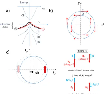
Figure 4. (color online) (a) Schematics of the Ge(111) elec-tronic band structure (in agreement with Ref. 21) showing the bulk conduction and valence bands. The Fermi level is at a position corresponding to a p-doped film. Subsurface states are located just above the maximum of the bulk valence band and are crossed by the Fermi level. They are spin-splitted by the Rashba and atomic spin-orbit interactions. (b) Fermi contours of the subsurface states. The outer (inner) contour is named C (D) with clockwise (counter-clockwise) spin he-licity. (c) Illustration of the combined effects of the applied magnetic field B and the current dependent pseudo-magnetic field BE on the resistivity of subsurface states for a single
contour (D here). The contour is shifted by + ∆k due to the application of a current density j along + ˆx. The current direction and spin helicity set the pseudo-magnetic field BE.
4
in the data shown in Figs. 1−3, the current flows along the ΓM direction of the Ge(111) SBZ, but no difference, within the experimental error, is detected with the cur-rent flowing along other reciprocal lattice directions (see Supplementary Material). In Refs.13 and15, the mag-netoresistance is affected by the direction of the current flow in the SBZ, indicating that, in such a case, the UMR originates from the out-of-plane spin texture. In the case of Ge, this contribution appears to be negligible. We thus propose an alternative mechanism, in which the UMR in Ge(111), results from a combination of the applied mag-netic field and the current-induced pseudo-magmag-netic field in the spin-splitted subsurface states of Ge(111) shown in Fig.4(a). Ge(111) subsurface states are located close to the top of the valence bands and can only contribute to transport in p-type Ge(111) [21]. This interpretation is supported by the fact that we do not observe this ef-fect for n-type Ge(111) (see Supplementary Material). It also explains the gate voltage dependence of RUMR
in Fig. 3(d). Applying negative gate voltage shifts the Fermi level down into the valence band which leads to the activation of bulk conduction and RUMR ≈ 0 Ω for
Vg = −10 V. At variance, by ramping the gate
volt-age from −10 V to +10 V, the Fermi level shifts into the subsurface states thus increasing RUMR. Finally, this
in-terpretation also explains the temperature dependence of the UMR. By increasing the temperature, bulk conduc-tion in the valence band is activated and shorts the sub-surface states. Moreover, the Rashba spin-orbit coupling of ∼ 58 kB in Ge subsurface states [21] becomes
negli-gible with respect to kBT suppressing spin-momentum
locking.
For the Fermi level crossing the subsurface states as shown in Fig. 4(a), the Fermi contour is made of two concentric rings [C and D in Fig. 4(b)] with opposite spin helicities. To describe the magnetotransport inside the subsurface states, we consider the following model Hamiltonian :
H = −~2k2
2m∗ + α (k × σ) · ˆz + gµBσ· B, (1)
with ~ being the reduced Planck constant, m∗ the effec-tive mass of holes in the subsurface states, α the Rashba spin-orbit interaction, σ the vector of Pauli matrices, g the Land´e factor and µBthe Bohr magneton. When a 2D
charge current density j flows in the subsurface states, in the Boltzmann approach, the momentum acquires an extra component ∆k = βj with β = 4π/(evFkF), vF
and kF the Fermi velocity and wavevector we consider
(e = |e|). A well-known consequence of such shifts of Rashba Fermi contours is the Rashba-Edelstein spin po-larization [7] due to the unbalance between the opposite spin polarizations induced by the shifts in the same di-rection of the Rashba-splitted Fermi contours of oppo-site helicity. In parallel with the Rashba-Edelstein ef-fect, the shift ∆k introduces a current-induced
out-of-equilibrium energy term which, from Eq. 1, is equal to α(∆k × σ) · ˆz = αβ(z × j) · σ and acts on the spins as a pseudo-magnetic field BE= (αβ/gµB) ˆz × j. As
illus-trated in Fig. 4(c), for a current along ± ˆx with α > 0 , this field is directed along ± ˆy and proportional to the current density. In the presence of an applied magnetic field B, the spin of the subsurface states is submitted to B + BE, BE increasing or decreasing the effect of the y
component of B for currents either along + or - ˆx. In the same way, still for α > 0 for j along +ˆx and BE along ˆy
, there is addition or subtraction of the effects of B and BEfor opposite orientations of B along ˆy. The physics of
the UMR thus comes from the pseudo-field BE induced
by the out-of-equilibrium situation of a current flow and acting on the spins. We can go a little further by assum-ing that the AMR term shown in Fig.1(c)(the only MR in the limit j → 0) is also due to the effect of B on the spins. We thus follow Taskin et al. [29] who explain the AMR of Rashba systems by the re-introduction of some backscatterings by a partial re-alignement of the spins by B and we neglect contributions such as the effect of the Lorentz force on the trajectories. Then, in the situation of finite j, we add BE to B in the B2 term of the AMR
to derive the expression of UMR. The AMR term can be written as:
(∆R/R)AMR= −A B2 cos2(ϕ) = ABy2− A B2 (2)
Where A ≈ 0.004. Adding BEy = αβj/gµB to By, and
keeping only the terms of first order in j gives :
∆R/R = −AB2cos2(ϕ) + 2A(αβ/gµB) j B sin(ϕ) (3)
Where the second term, proportional to j B, is the UMR. Our experimental results with an UMR proportional to j B sin(ϕ), see [Fig.2], correspond to a negative value of the Rashba coefficient α, that is to the clockwise chirality of the spin orientation in the outer Fermi contour. This chirality is in agreement with the chirality derived from spin-resolved ARPES measurements for the subsurface states inside Ge at Ge/Bi interfaces, as shown in Fig. 3a of [20]. Quantatively, taking reasonable values for the parameters in the expression of the UMR amplitude. By setting B = 1 T, j = 0.33 A m−1 in the subsurface states, α = −0.2 eV · ˚A (in [20], this value corresponds to Bi covered subsurface states, in our case it is probably an upper bound), kF= 0.025 ˚A
−1
(Rashba splitting |αkF| =
5 meV∼ 58 kB), m∗= 0.4 me[28], mebeing the electron
mass, vF= ~kF/m∗and g = 2, we find a UMR amplitude
of ≈ 0.2%. This value is in good agreement with our low temperature experimental data. We indeed find a maximum value of 0.5% at 15 K. Therefore, by using simple arguments, we capture the physics of UMR in the Ge Rashba-splitted subsurface states.
In conclusion, we performed magnetoresistance mea-surements on Ge(111) and detected a unidirectional mag-netoresistance (UMR) which scales linearly with both the
current and the applied magnetic field. We ascribe the UMR to the spin-momentum locking generated by the Rashba effect in the subsurface states of Ge(111) and in-terpret our results in a simple model relating the UMR to the Rashba coefficient and the characteristic param-eters of the subsurface states. Such unidirectional ef-fects can be expected in any Rashba 2DEG and can be used to obtain information about the electronic struc-ture details. The amplitude of the detected UMR signal is much larger than the ones previously reported. We also showed that this UMR is tunable by turning on and off the Rashba coupling in the conduction channel by applying a gate voltage. Ultimately, these findings lead towards the development of a semiconductor-based spin transistor where the spin information can be manipulated by a gate-tunable Rashba field.
The authors acknowledge the financial support from the ANR project ANR-16-CE24-0017 TOPRISE. One of us (AF) acknowledges fruitful discussions with A .Dyrdal and J. Barnas (Poznan University), as well as with S. Zhang (University of Arizona).
[1] J. ˚Akerman, Science 308, 508 (2005).
[2] M. N. Baibich, J. M. Broto, A. Fert, F. NguyenVanDau, F. Petroff, P. Etienne, G. Creuzet, A. Friederich, and J. Chazelas, Phys. Rev. Lett. 61, 2472-2475 (1988). [3] G. Binasch, P. Gr¨unberg, F. Saurenbach, and W. Zinn,
Phys. Rev. B 39, 4828(R)-4830(R) (1989). [4] H. Ohno, Science 281, 951-956 (1998).
[5] T. Dietl, H. Ohno, F. Matsukura, J. Cibert, D. Ferrand, Science 287, 1019-1022 (2000).
[6] L. Chen, X. Yang, F. Yang, J. Zhao, J. Misuraca, P. Xiong, S. von Moln´r, Nano Lett. 11, 2584-2589 (2011). [7] C. Chappert, A. Fert, and F. N. Van Dau, Nat. Mater.
6, 813 (2007).
[8] A. Manchon, H. C. Koo, J. Nitta, S. M. Frolov, and R. A. Duine, Nat. Mater. 14, 871 (2015).
[9] N. Locatelli, V. Cros, and J. Grollier, Nature Mater. 13, 11-20 (2014).
[10] J. Kim, P. Sheng, S. Takahashi, S. Mitani, and M. Hayashi, Phys. Rev. Lett. 116, 097201-097206 (2016). [11] I. Latella, and P. Ben-Abdallah, Phys. Rev. Lett. 118,
173902-173907 (2017).
[12] Z. Qiu, D. Hou, J. Barker, K. Yamamoto, O. Gomonay, and E. Saitoh, Nature Mater. 17, 557-580 (2018). [13] P. He, S. S.-L. Zhang, D. Zhu, Y. Liu, Y. Wang, J. Yu, G.
Vignale, and H. Yang, Nature Phys. 14, 495-499 (2017). [14] S. S.-L. Zhang, G. Vignale, arXiv:1808.06339v1 (2018). [15] P. He, S. M. Walker, S. S.-L. Zhang, F. Y. Bruno, M.
S. Bahramy, J. M. Lee, R. Ramaswamy, K. Cai, O. Heinonen, G. Vignale, F. Baumberger, and H. Yang, Phys. Rev. Lett. 120, 266802-266807 (2018).
[16] K. Olejnik, V. Nov´ak, J. Wunderlich, and T. Jungwirth, Phys. Rev. B 91, 180402(R)-180407(R) (2015).
[17] C. O. Avci, K. Garello, A. Ghosh, M. Gabureac, S. F. Alvarado, and P. Gambardella, Nature Phys. 11, 570-575 (2015).
[18] K. Yasuda, A. Tsukazaki, R. Yoshimi, K. S. Takahashi, M. Kawasaki, and Y. Tokura, Phys. Rev. Lett. 117, 127202-127207 (2016).
[19] Y. Lv, J. Kally, D. Zhang, J. S. Lee, M. Jamali, N. Samarth, and J.-P. Wang, Nature Commun. 9, 111 (2018).
[20] Y. Ohtsubo et al., Phys. Rev. B 82, 201307(R) (2010). [21] Y. Ohtsubo, K. Yaji, S. Hatta, H. Okuyama, and T.
Aruga, Phys. Rev. B 88, 245310-245317 (2013).
[22] T. Aruga, J. Electron Spectrosc. Relat. Phenom. 201, 74-80 (2015).
[23] K. Yaji, Y. Ohtsubo, S. Hatta, H. Okuyama, R. Yukawa, I. Matsuda, P. Le F`evre, F. Bertran, A. Taleb-Ibrahimi, A. Kakizaki, and T. Aruga, J. Electron Spectrosc. Relat. Phenom. 201, 92-97 (2015).
[24] C. Zucchetti, F. Bottegoni, C. Vergnaud, F. Ciccacci, G. Isella, L. Ghirardini, M. Celebrano, F. Rortais, A. Ferrari, A. Marty, M. Finazzi, and M. Jamet, Phys. Rev. B 96, 014403-014408 (2017).
[25] F. Rortais et al., Appl. Phys. Lett. 111, 182401 (2017). [26] V. M. Edelstein et al., Solid State Comm. 73, 233 (1990). [27] T. Ozturk, R. L. Field III, Y. S. Eo, S. Wolgast, K. Sun,
and C. Kurdak, arXiv:1412.1007v2 (2014). [28] See: http://www.ioffe.ru
[29] A.A. Taskin, H. F. Legg, F. Yang, S. Sasaki, Y. Kanai, K. Matsumoto, A. Rosch, and Y. Ando, Nat. Commun. 8, 1340 (2017).