HAL Id: hal-01122589
https://hal.archives-ouvertes.fr/hal-01122589
Submitted on 4 Mar 2015HAL is a multi-disciplinary open access archive for the deposit and dissemination of sci-entific research documents, whether they are pub-lished or not. The documents may come from teaching and research institutions in France or abroad, or from public or private research centers.
L’archive ouverte pluridisciplinaire HAL, est destinée au dépôt et à la diffusion de documents scientifiques de niveau recherche, publiés ou non, émanant des établissements d’enseignement et de recherche français ou étrangers, des laboratoires publics ou privés.
Auger electronic spectroscopy and electrical
characterisation of InP(100) surfaces passivated by N2
plasma
Matthieu Petit, Christine Robert-Goumet, Luc Bideux, Bernard Gruzza, Z
Benamara, N Bachir Bouiadjra, V Matolin
To cite this version:
Matthieu Petit, Christine Robert-Goumet, Luc Bideux, Bernard Gruzza, Z Benamara, et al.. Auger electronic spectroscopy and electrical characterisation of InP(100) surfaces passivated by N2 plasma. Applied Surface Science, Elsevier, 2004, 234 (1-4), pp.451-456. �10.1016/j.apsusc.2004.05.029�. �hal-01122589�
Auger electronic spectroscopy and electrical characterisation of
InP(100) surfaces passivated by N
2plasma
M. Petita, Ch. Robert-Goumeta*, L. Bideuxa, B. Gruzzaa, Z. Benamarab
N. Bachir Bouiadjrab, V. Matolinc
aLASMEA, UMR 6602, Blaise Pascal University, 63177 Aubiere cedex, France.
bAMEL, Djillali Liabes University, 22 000 Sidi Bel Abbes, Algeria.
cDepartment of Electronics and Vacuum Physics, Charles University, V Holesovickach 2,
180 00 Prague 8, Czech Republic.
* Corresponding author : tel : +33 4 73 40 76 49, fax : + 33 4 73 40 73 40, e-mail : [email protected]
PACS : 77.84.B; 82.80.P; 68.55.J; 73.61.E
Keywords : AES; Indium phosphide(100); Indium nitride; electrical measurements.
Abstract :
Auger electron spectroscopy (AES) was used to investigate the processes taking place during the initial stages of InP(100) surfaces nitridation. This AES study combined with electrical measurements (intensity-potential) shows that the processes greatly differ depending on the nitridation angles. Results show that with grazing angle for nitrogen flow, the nitridation process is more efficient. Results obtained with AES spectra are coherent with electrical measurements : Hg/InN/InP(100) Schottky diodes present better electrical characteristics in the case of a grazing flow. That means, the adsorption of nitrogen on the surface is more important for this configuration.
Introduction :
Group III-nitride semiconductors are promising wide band-gap materials for micro and optoelectronic devices since nitride alloys can cover the full visible spectra – from near
infrared (Eg= 0,9 eV for InN [1-2]) to the far ultraviolet (Eg=6,2 eV for AlN [3]).
The InP surfaces nitridation has different interests as the realisation of InN buffer layers before the InN films growth, or as passivated layers. Indeed, no protective material
exist for III-V semiconductors as SiO2 on Si. On the contrary, the presence of In2O3 or InPO4
on InP surfaces produces important degradation for the electrical properties of the structures. That is why the surface passivation is one of the most important processes in the fabrication of InP-based electronic and optoelectronic devices. Different methods have been employed for the nitridation of InP(100) surfaces :
- by N2+ ions beam bombardment [4-5-7]
- by plasma nitridation [6]
It is known that the nitrogen parameters influence the structural and electronic properties of the nitridated surfaces. For instance, previous works [4] have shown that the normal incidence
provides maximum efficiency of ion incorporation for N2+ ions beam bombardment (energy
range between 0,3 and 1 keV)
In this paper we proposed to investigate the influence of the incident angle of the nitrogen flow produces with a plasma source. This nitridation process is monitored by Auger electron
spectroscopy. We also compare the different current-tension electrical measurements of samples nitridated by different angles.
Experimental procedures:
S-doped InP(100) samples have been used, they were chemically cleaned ex-situ with
successive ultrasonic baths [8] (H2SO4, 3% bromine–methanol desionised water) before
introduction in an ultra high vacuum chamber (10-6 to 10-7 Pa). InP(100) surfaces have been
cleaned by in-situ Ar+ ionic bombardment before the nitridation. This ionic cleaning leads to
two phenomena : the removal of the contamination layers mainly due to carbon species [9], and the creation of metallic indium droplets in well controlled quantity by preferential phosphorus sputtering [10-11].
These indium droplets will play a key role during the nitridation process. The surface state is monitored by EPES combined with AES [9]. All the in situ experiments have been driven with a retarding field analyzer (OPR 309 Riber).
The nitridation process has been performed with a high voltage plasma discharge cell (glow discharge source (GDS)) to create one or two monolayers of InN on InP(100) substrates through the consumption of indium droplets by nitrogen. In this kind of nitrogen source, a continuous plasma is produced by a high voltage (about 2 kV). A majority of N atomic species
are created. However some amount of N2+ is produced but the energy of ions is very low (few
eV). Two angles have been studied for the nitrogen flow : 0° (normal incidence) and 80° (grazing incidence) versus the normal of the surface. Low temperature processing is essential
in nitridation of InP, indeed the InP decomposition temperature is about 350°C.The substrate
is heated to 250°C during the nitridation process, according to previous work investigating the influence of the temperature on the nitridation process [12].
Results and discussion :
1- Auger analysis :
The nitridation of InP (100) substrates was studied using Auger spectroscopy (AES). The measurements have been carried out simultaneously with the nitridation process. To characterise the chemical bonding and composition of the buffer layer growing during the process, the Auger signals of In-MNN, P-LMM and N-KLL transitions at about 403 eV and 411 eV, 117 eV and 383 eV respectively have been used.
Evolution of the nitrogen Auger peak (N-KLL):
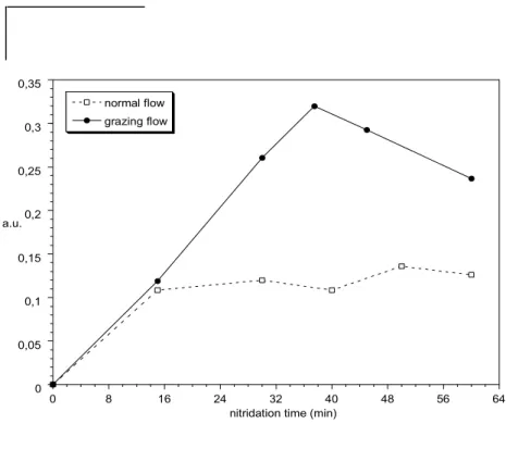
During the nitridation process, the nitrogen Auger signal for the two incident angles of the nitrogen flow has been monitored (figure 1). An increased of this signal is put in evidence. However, we observed a difference between the maximum of Auger intensity between the two angles. For the normal angle, a step is reached from 15 minutes of nitridation time. On the contrary, for the grazing angle, the nitrogen Auger intensity is higher and reaches a maximum at 40 min of nitridation time. After 40 minutes, the N Auger intensity decreases, probably due to a destruction of nitride layers. This first observation can give us the following information : the nitridation process seems to be more efficient with a grazing incident nitrogen flow on the surface.
We have calculated two ratios RPIn and RPN which have been defined in previous work
[9, 13].
We just remind that the phosphorus Auger peak can be decomposed into three gaussians corresponding to P-In bonds before nitridation and into two groups of three gaussians after nitridation : the first group is related to P-In bonds and the second group to the P-N bonds.
RPIn gives information about the amount of P-In bonds and RPN, information about the quantity
of P-N bonds produce during the nitridation process.
Figure 2 shows the evolution of these two ratios during the nitridation time and for the two incident angles of the nitrogen flow. The graph can be decomposed into three parts :
- from 0 to 35 min, RPIn decreases and RPN increases in the both angles with RPIn > RPN : P-N
bonds increases but P-In bonds are still the most numerous.
- Between 35 and 42 min, RPIn < RPN : the quantity of P-N bonds is higher than the P-In
bonds but in the same range for the two angles.
- After 42 min, RPIn becomes greater than RPN once again but the discrepancy is more
important in the case of normal angles than in the case of the grazing angle.
This phenomena is attributed to the damaging of the surface under the etching effect of the impinging nitrogen flow.
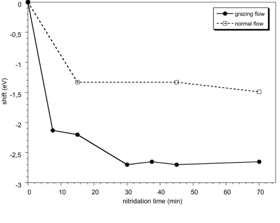
Observation of the Indium Auger shift :
Figure 3 represents the shift of the indium Auger spectra. The low-kinetic energy shift is more pronounced during the 10-15 first minutes of the nitridation. This shift can be explained by a change in the chemical environment of the indium atoms on the surface. During this short interval, the incoming N atoms substitute for the P atoms and the formation of P-N compound is responsible for the observed Auger shift. Indeed, the ionicity of the In-N bonds is higher than that of the In-P bonds due to an increased charge transfer from the In to anion as phosphorus is substituted by nitrogen [14]. We remind the value of Pauling electronegativity of P and N : 2,19 and 3,04 respectively. A shift of the core levels of In to higher binding energies is expected and then a low kinetic energy shift of the In-MNN Auger transition can be observed.
We observed a great difference between the two flow angles. The shift is more pronounced for the grazing incident flow than for the normal one. It means that the chemical environment of the indium atoms is higher N content.
To conclude, the Auger spectroscopy demonstrates that the maximum of the nitridation process is around 40 minutes for both incident angles. The P Auger peaks study shows that for the two angles, there is formation of P-N bonds. But N Auger peaks and In shift seem to prove that the nitridation is more efficient in the case of grazing nitrogen flow.
After 40 minutes, we observe a decreasing of the P-N bonds and of the quantity of N atoms for the grazing angle. We think it is caused by the destruction of the nitride layers. This damaging may be due to several phenomena which take place simultaneously : dissociation of the substrate surface under temperature [15], evaporation of the layers and sputtering effect of the nitrogen flow. The last phenomenon seems to be weaker for the grazing flow. Further XPS analysis are necessary for a better understanding of this damaging process.
peak phosphorus the of area total gaussians In P of area RPIn
peak phosphorus the of area total gaussians N P of area RPN
2- Electrical I(V) measurements :
The Hg/InN/InP Schottky diodes –where “InN” is the nitride layers created by the nitridation process- were characterised by electrical measurements (I-V). InP substrates
nitridated during 60 min have been used. Parameters like the saturation current Is, the barrier
height BN, the serial resistance Rs have been calculated from log(I) = f(V) and I(V) curves
and are summarised in table 1.
The expression which connects the intensity I to the applied potential V is : [16-17]
s
s B q× V-R ×I I(V)=I ×exp n×k ×T where :V is the direct applied voltage ; n is the mean ideality factor ;
RS is serial resistance of the structure ;
T is the temperature ;
kB is the Boltzman constant
IS is the saturation current.
The barrier height BN is given by :
* 2 BN S A T Φ =kT ln J Where :
A* is the Richardson constant ;
JS is the surface density current.
To extract the electrical parameters from the experimental characteristics, we have considered
the part of weak polarization (figure 4) from which we determined the saturation current IS
which corresponds to a null bias voltage. The shift between the curve of weak bias voltage and that of high biasing gives RS value. The diffusion potential Vd corresponds to the
equilibrium of the structure (I = 0) and is quoted to the I(V) curve.
The direct and reverse I(V) characteristics are shown in figure 4 for both normal and grazing angles. The direct currents have exponential forms. The direct current for the grazing flow is higher. The electrical properties of the Hg/InN/InP Schottky diodes are influenced by the nitridation process. It means that the passivation effect of the nitride layer is different with the incident nitrogen flow angle.
Conclusions :
The processes taking place during the nitridation of InP(100) surfaces greatly differ depending on the incident angle of the nitrogen flow. Auger spectra demonstrate that the grazing flow is more efficient : the amount of nitrogen is greater, the shift of indium auger peak is more important showing that the chemical environment of the indium atoms is richer
weaker with the grazing flow, the nitride layers are less damaged. We also observed significant differences between grazing and normal flow with electrical measurements : These observations prove that the passivation effect of the nitride layers depends on the incident nitrogen angle flow.
References :
[1] V. Yu. Davydov, A. A. Klochikhin, R. P. Seisyan, V. V. Emtsev, S. V. Ivanov, F. Bechstedt, J. Furthmüller, H Harima, A. V. Mudryi, J. Aderhold, O. Semchinova, J. Graul, Phys. Stat. Sol. (b), 229, No 3, R1-R3 (2002).
[2] F. Bechstedt, J. Furthmüller, J. Cryst. Growth, 246 (2002) 315-319. [3] B. Monemar, J. Mat. Sci. : materials in electronics 10 (1999) 227-254.
[4] J. S. Pan, A. T. S. Wee, C.H.A. Huan, H.S. Tan, K.L. Tan, J. Phys. D : Appl. Phys. 29 (1996) 2997-3002,
[5] Y. Suzuki, H. Kumano, W. Tomota, N. Sanada and Y. Fukuda, Applied
Surface Science 162-163 (2000) 172-177
[6] M. Losurdo, P. Capezutto, G. Bruno, G. Leo, E.A. Irene, J. Vac. Sci.
Technol. A 17 (4), (1999) 2194-2201
[7] G. Beuchet, M. Bennet, P. Thebault, J. P. Duchemin, J. Cryst. Growth 54 (1982), 379. [8] J. D. Hect, F. Frost, T. Chassé, D. Hirsch, H. Neumann, A. Schindler, F. Bigl, Appl.
Surf. Sci. 179, (2001), 196-202.
[9] M. Petit, Y. Ould-Metidji, Ch. Robert, L. Bideux, B. Gruzza, V. Matolin, Applied Surface Science 212–213 (2003) 601–606
[10] B. Gruzza, L. Bideux, P. S. Mangat, P. Soukiassian, Synth. Met. 90 (1997) 223-227 [11] P. S. Mangat, P. Soukiassian, Y. Huttel, Z. Hurych, B. Gruzza, A. Porte, Appl. Phys.
Lett 63(14) (1993) 1957-1959.
[12] L. Bideux, Y. Ould-Metidji, B. Gruzza, V. Matolin, Surface and Interface Analysis Vol. 34, Issue 1, 2002, 712-715
[13] Y. Ould-Metidji, L. Bideux, V. Matolin, B. Gruzza, C. Robert, Vacuum
63 (2001) 229-232
[14] I. Aksenov, Y. Nakada, H. Okumura, MRS Internet J. Nitride Semicond. Res. 4S1, G3.4 (1999)
[15] R. F. C. Farrow, J. Phys. D : Appl. Phys., vol. 7, 1974, L121-L124
[16] B. Akkal, Z. Benamara, A. Boudissa, N. Bachir Bouiadjara, M. Amrani, L. Bideux, B. Gruzza, Materials Science and Engineering B, Vol. 55, Issue 3, (1998), 162-168. [17] S. M. Sze, Physics of semiconductors devices, Wiley & Sons Editor, New York, 1981.
Figures and tab caption
Tab 1 : Electrical parameters calculated from log I(V) and I(V) curves of the Hg/InN/InP Schottky diodes.
Figure 1 : Evolution of the intensity of the nitrogen Auger Peak during the nitridation time for the two incident angles of the nitrogen flow.
Figure 2 : Variation of the ratios RPN and RPIn according to the incident angle of the nitrogen
flow.
Figure 3 : Variation of the shift of the indium Auger peak.
Figure 4 : log I = f(V) curves of the Hg/InN/InP Schottky diodes for the normal and grazing nitrogen flows. Inset : I(V) curves.
Bn (eV) Is (A) Vd (V) Rs ()
InP (Grazing) 0.66 6 10-5 2.16 50
InP (Normal) 0.85 3.16 10-8 2.43 340
Figure 1 0 0,05 0,1 0,15 0,2 0,25 0,3 0,35 0 8 16 24 32 40 48 56 64 normal flow grazing flow a.u.
Figure 2 0 0,2 0,4 0,6 0,8 1 0 10 20 30 40 50 60 70 R(P-In) grazing R(P-N) grazing R(P-In) normal R(P-N) normal R ( a. u)
Figure 3 -3 -2,5 -2 -1,5 -1 -0,5 0 0 10 20 30 40 50 60 70 grazing flow normal flow sh ift ( eV )
Figure 4 -10 -8 -6 -4 -2 0 0 0,5 1 1,5 2 2,5 3 3,5 4
log I (normal incidence) log I (grazing incidence)
lo g (I ) bias voltage (V) 0 0,0122 0,0244 0,0366 0,0488 -3,36 -1,68 0 1,68 3,36 I (A ) bias voltage (V)