Design of Optoelectronic Activation, Local
Memory and Weighting Circuits for Compact
Integrated Optoelectronic Neural (COIN)
Co-processor
by
Wegene Haile Tadele
B.S,
Massachusetts Institute of Technology (2014)
Submitted to the Department of Electrical Engineering and Computer
Science
in partial fulfillment of the requirements for the degree of
Master of Engineering in Electrical Engineering and Computer Science
at the
MASSACHUSETTS INSTITUTE OF TECHNOLOGY
September 2015
@
Massachusetts Institute of Technology 2015. All rights reserved.
Signature redacted
A uthor ...
Department of Electrical Engineeringand Computer Science
July 27, 2015
Certified by...
Signature redacted
I -~
Cardinal Warde
Professor
Thesis Supervisor
Accepted by ...
Signature redacted ...
er.
Jr4
christopher
J.Terman
Chairman, Department Committee on Graduate Theses
M SACHUSETS INSTIT -TE
FC TCHNOLOGY
AUG
018
/f.BRARIES
/S MASSACHUSETTS INSTITUTE OF TECHNOLOGYJUL 19 2016
MITLibraries
77 Massachusetts Avenue
Cambridge, MA 02139 http://Iibraries.mit.edu/ask
DISCLAIMER NOTICE
Due to the condition of the original material, there are unavoidable flaws in this reproduction. We have made every effort possible to provide you with the best copy available.
Thank you.
Despite pagination irregularities, this is the most complete copy available.
* Thesis is missing pages 7-8
This Master of Engineering thesis has been examined by a Committee
of the Department of Electrical Engineering and Computer
Science(EECS) as follows:
Dr. Christopher J.Terman ...
Professor Cardinal Warde...
Signature redacted
Chairman, tYsis Committee
Professor of EECS
Signature redacted
Thesis Supervisor
Professor of EECS
Design of Optoelectronic Activation, Local Memory and
Weighting Circuits for Compact Integrated Optoelectronic
Neural (COIN) Co-processor
by
Wegene Haile Tadele
Submitted to the Department of Electrical Engineering and Computer Science on July 27, 2015, in partial fulfillment of the
requirements for the degree of
Master of Engineering in Electrical Engineering and Computer Science
Abstract
The Compact Integrated Optoelectronic Neural (COIN) Co-processor, a prototype of artificial neural network implemented in hybrid optics and optoelectronic hardware, aims to implement a multi-layer neural network algorithm by performing parallel and efficient neural computations. In this thesis, we design and implement optoelectronic thresholding (activation), weighting and memory circuits for the COIN processor. The first version involved the design of fixed thresholding and weighting functions. The second version incorporated a local capacitive memory element as well as variable weighting schemes. The third version introduces an additional flexibility for variable thresholding by changing the bias voltages of control transistors. A 9x9 array of proof of concept printed circuit board (PCB) with an area of 4.5x 4.5 in2 and total power
consumption of 1.37W was designed and tested for version-I optoelectronic neuron architecture. A spice simulation was performed for the last two versions for integrated circuit (IC) implementation. The work developed in this thesis provides some guid-ance on the design of optoelectronic neural activation function for the realization of the embodiment of the fully integrated COIN Co-processor to be built in the future. Thesis Supervisor: Cardinal Warde
Title: Professor
Acknowledgments
I would not be here without the support of so many people. First and foremost, I would like to thank my thesis supervisor Prof. Cardinal Warde. His continued
support during my undergraduate and graduate research work at MIT has helped me grow both personally and professionally. Next, I would like to thank William Herrington for his invaluable advice and insight during the course of this research.
My sincere gratitude goes to my grandmother, Kuri Woldeyes, in my hometown
in the South Central Ethiopian countryside. Without her unconditional support and sacrifice, nothing else would have been possible. My parents Damenech Kifle and Tadele Haile have always been my inspirations. My mother's wise advice and my father's encouragement to use my full potential have played an indispensable role in helping me accomplish my goals and ambitions. I would also like to thank my siblings Zenebe, Dawit, Abel, Mintesinot, Edelawit and Samrawit for their moral support and boosting my confidence. My utmost gratitude goes to the Perry Family especially to Barbara, Joan and Jimbo Perry for their loving parental support and helping me grow personally and spiritually. I would also like to thank Park and Whitley Morris for supporting me financially during my undergraduate education.
Furthermore, I would like to thank my valued friends Abiy Tassisa and Iyob Gebre-mariam. Their continued support both in and out of school has played a substantial role in my academic and professional endeavors. Moreover, I would like to thank ev-eryone whose names are not mentioned here but have been part of my success journey directly or indirectly. Last but not least, I would like to thank my amazing girlfriend Natalie Strong for her encouragements and tirelessly reviewing my thesis.
MITLibraries
77 Massachusetts Avenue Cambridge, MA 02139 http://Iibraries.mit.edu/askDISCLAIMER NOTICE
MISSING PAGE(S)#7
MITLibraries
77 Massachusetts Avenue Cambridge, MA 02139 http://Iibraries.mit.edu/askDISCLAIMER NOTICE
MISSING PAGE(S)#8
Contents
1 Introduction 21
1.1 Background on Neural Computing . . . . 22
1.1.1 Artificial Neuron Model . . . . 24
1.1.2 Learning in ANNs and Training Algorithms . . . . 26
1.2 The COIN Co-Processor and Hardware Implementation of Artificial Neural Networks . . . . 27
1.3 Thesis Summary . . . . 30
2 The COIN System 33 2.1 Background on Compact Optoelectronic Integrated Neural (COIN) Co-processor . . . . 33
2.2 COIN Component Considerations . . . . 34
2.2.1 Photodetector Considerations . . . . 35
2.2.2 The Threshold Circuit . . . . 38
2.2.3 Driver circuits and weight storage elements . . . . 38
2.2.4 Output Light Sources . . . . 38
2.2.5 Optical Interconnects for COIN . . . . 40
2.3 Previous Work on Neural Activation Functions and Weighting Circuits 41 2.3.1 Optoelectronic Neuron Circuit with Variable Synaptic Weights 41 2.3.2 Digital-Analog Hybrid Synapse Chips for Electronic Neural Net-w orks . . . . 43
3 Mathematical Models of Different Types of Activation functions 47
3.1 3.2 3.3
3.4
3.5
Generalized Thresholding Function . . . . The Sigmoidal Function . . . . The Arc Tangent Activation Function . . . . The Hyperbolic Tangent Activation Function . . . . Comparison of Neural Activation Functions . . . . 4 Activation Function Circuit for COIN: Version-I
4.1 Implementation of Optoelectronic Neuron for Version-I . . . . 4.1.1 LED Characterization and Selection . . . .
4.1.2 MOSFET and LED Modeling and Characterization . . . .
4.1.3 Phototransistor Modeling and Characterization . . . .
4.2 Version-I Optoelectronic Neuron Circuit . . . . 4.3 The 9x9 Array of Optoelectronic Neuron Implementation in Discrete
Components 4.3.1 4.3.2 Result . . . . Discussion . . . . 48 49 50 51 52 55 58 65 67 69 71 73 74 75
5 Improved Circuit Architectures for COIN: Versions-II and III 77
5.1 COIN Model for the improved circuit Architecture . . . . 78
5.2 Low-Level Block Diagram of a Pixel . . . . 79
5.3 Neural Weighting and Associative Memory Circuits . . . . 80
5.4 Optoelectronic Neuron Model for Version-I . . . ... . 82
5.5 Spice Simulation Results for version-II . . . . 83
5.6 Optoelectronic neuron model for version-III . . . . 85
5.6.1 Subthreshold MOSFET Operation . . . . 85
5.6.2 Differential Pair . . . . 86
5.6.3 Current M irrors . . . . 87
5.6.4 Operational Transconductance Amplifier(OTA) . . . . 88
5.6.5 The Optoelectronic Neuron Model of Version III . . . . 90
5.7 Spice Simulation Results for version-III . . . . 90
5.8 Recommendation for Integrated Circuit (IC) Layout . . . . 92 10
5.9 Limitations on Circuit Design and Neuron Density . . . .9
6 Conclusions 95
6.1 Summary of Contributions . . . . 95
6.2 Applications . . . .. . . . . 96
6.3 Discussion of Future Work . . . . 97
11
List of Figures
1-1 Structure of Biological Neurons: Presynaptic and postsynaptic neurons[61] 23 1-2 A three layer network: stimulation is applied to the inputs of the first
layer, and signals propagate through the hidden layer to the output layer. Each connection between neurons has a unique weighting value. 25
1-3 Artificial Model of Neuron . . . . 25
1-4 Schematic architecture of a multilayer optical neural network. Each circle represents a neuron while a filled circle means that the neuron is in the "ON" state . . . . 29
2-1 A Block Diagram of a three layer COIN Co-processor system. Adopted from the work of Travis Simpkins[56]. Each layer consists of arrays of photodetectors, optical interconnection elements and thresholding circuits . . . . 34
2-2 A Diagram of a COIN neuron . . . . 35
2-3 Lump-sum equivalent-circuit model of a photodiode . . . . 36
2-4 Phototransistor Equivalent Circuit . . . . 37
2-5 Optoelectronic neuron circuit and synaptic connection (Ti3 cell). a) Ba-sic neuron circuit. Photocurrent Ij flows from MOSFET Q1 to PD for excitatory connection, and flows in inverse direction for inhibitory con-nection. b) Photo-currents for excitatory and inhibitory connections. Bipolar Tij values were obtained by following combination. Adapted from [66] . . . . 42
2-6 ... ... .. ... 42
2-7 Primitive optoelectronic CAM circuit with 4 x 4 network. Adapted
from [66] . . . . 43
2-8 Simplified block diagram of hybrid 32x32x7-bit synapse chip. Adapted
from [38] . . . . 44
2-9 Block diagram of 7-bit multiplying DAC. Adapted from [38]. . . . . . 44
2-10 Transfer characteristics of a 7-bit synapse for weight values of 0
+/-1,
3, 7, 15, 31, 63 (a) with long channel transistors and (b) with external
1OMQ for voltage to current conversion. Adapted from [38]. . . . . . 45
2-11 Electronic circuit neuron model and synapses. Where V is the output of the neuron i, Ti is the synaptic weight from neuron
j
to neuron i, R1 and Cf are the feedback capacitance and resistance of the neuron, and Ii is the external input current. RF and Cf should be chosen to ensure stability against oscillations. Adapted from [38]. . . . . 453-1 Plots of generalized thresholding function plotted at three biases and
rise speeds. a) Generalized activation function responses at three dif-ferent bias points of B=0,1, and 3. b)Responses at three difdif-ferent rise speed of V= 2, 3.33 and 2.5. Only one of these parameters are varied for a given plot. . . . . 49
3-2 a) Plots for different values of the rise speed(). b) The sigmoidal
function for three different bias values (B). The bias value in the opto-electronic activation corresponds to the turn on voltage of the transistor 50
3-3 a) A plot of arc-tangent function for three different lateral shift (zero
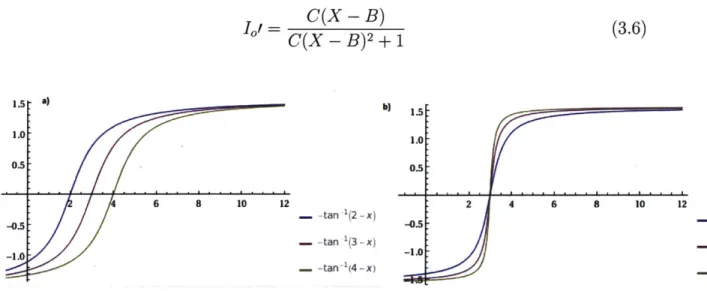
crossing) values. The zero crossing values specified by B are 2, 3 and 4. b) The response of arc-tangent thresholding function at fixed bias point B for three different values of rise speed (C). The value of B is 3 and the rise speeds for each curve are specified in the equations . . . 51
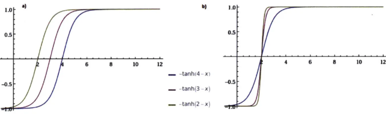
3-4 a) The plot of hyperbolic tangent function three different lateral shift values(B). The lateral shift(B) corresponds to the zero crossing or the thresholding point in this function. b) A plot of hyperbolic tangent function for three different values of rise speed(C) . . . . 52 3-5 a) Plots of the three thresholding functions; sigmoidal, hyperbolic
tan-gent and arc-tantan-gent functions. The sigmoid function goes from 0 to
1 and the arc-tangent and hyperbolic tangent functions go from -1 to 1. b) The derivatives of the three functions which is the same as the
error. We can compare the convergence speed of the error associated with each function from the plot . . . . 53
4-1 Block Diagram of one pixel of the COIN Co-processor for Version-I Optoelectronic neuron circuit: Interconnects driven by one light source per neuron and modulated by a Spatial Light Modulator(SLM) . . . 55
4-2 A signal flow diagram between layers of neurons. Adopted from [56] . 56
4-3 The inputs and outputs of a single neuron are represented by the cen-tral circle. Each rectangle associated with some weight represents a synapse, such that a neuron and a succeeding synapse comprises one pixel of the proposed COIN Co-processor. The preceding synapses are also associated with pixels in the preceding neuron layer. . . . . 57
4-4 An Optoelectronic Neuron Circuit: VDD is supply voltage, VB1 and VB2 are bias voltages for transistors M1 and M3 respectively. The voltages are generated such that the two transistors operate in triode region. These two transistors can also be replaced with a fixed resistor 59
4-5 Photodarlington transistor pair. PT1= Phototransistori and PT2= Phototransistor2 . . . . 61
4-6 MOS resistor operated in triode region . . . . 63
4-7 (a)LED characterization circuit, and (b)a plot of LED current vs. Rel-ative output intensity . . . . 66
4-8 (a)MOSFET and LED characterization circuit, and (b)a plot of gate voltage(VGate) vs. Relative output intensity . . . . 67
4-9 (a)Relative output intensity (Iot) vs. gate voltage (VGate) (b)Output
LED current (io0 t) vs. gate voltage(VGate) c) Relative output intensity
(Iout) vs. output LED current (iout) . . . . 68
4-10 (a).Phototransistor characterization circuitry setup. (b) Relative input intensity vs. Phototransistor emitter current. (c) The non-saturated section of plot (b). The polynomial fit was done only for the non-saturated section of plot (b) since that is the only region of interest for this application. . . . . 70
4-11 An Optoelectronic Neuron Test Circuit. The input light source was placed 4.5 cm away from the phototransistor and at the angle of maximum-beam divergence of the LED . . . . 72
4-12 Relative output intensity ('out) vs.Emitter current of the phototransis-tor (ii,). Raw data is shown in dotted lines and the sigmoidal fit is shown in solid lines. The sigmoidal fit was achieved using a function of the form y =..+e...-..> ...'.' ...-.'...'.'...'...'.'.'.'...7
4-13 9x9 Optoelectronic Neuron Array PCB front. The front plane consists of arrays of output LEDs and MOSFETs . . . . 74 4-14 9x9 Optoelectronic Neuron Array PCB back showing the
phototran-sistors array and rephototran-sistors. . . . . 74 4-15 Input of 5. 5 is presented as an input to the 2-D array of optoelectronic
neurons. The brightness is adjusted with the polarizers . . . . 75
4-16 Output of 5. The output is generated by activating the corresponding neurons in the 2-D array of optoelectronic neurons . . . . 75
5-1 COIN Block diagram of Versions-II and III electronic circuits: Inter-connects driven by individual sources and modulated by controllable driver circuits . . . . 78
5-2 Block Diagram of one pixel of the COIN Co-processor for Version-I
Optoelectronic neuron circuit: Interconnects driven by one light source
per neuron and modulated by a Spatial Light Modulator(SLM) . . . 79
5-3 A Pixel. wi corresponds to weights stored in local memory elements. C corresponds to the optical interconnection element used for inter-plane com m unication. . . . . 80
5-4 A Basic short term memory circuit implemented using sample-and-hold circu it . . . . 82
5-5 Version-Il Optoelectronic neuron model with capacitive local memory element. Weights are periodically updated from the stored weight el-ements. ist_ and outx correspond to the output current and relative output intensity of synapse x respectively. ii, is the photogenerated current of the pixel from external illumination. . . . . 83
5-6 Version-II optoelectronic neuron: A schematic with three synapses used to obtain simulation plots . . . ... 84
5-7 Plots for various weights. The three synapses have three different weights that are controlled by the voltage divider at the gate of the output M OSFET. . . . . 84
5-8 Differential Pair . . . . 87
5-9 Current M irrors . . . .. . . . 88
5-10 Operational Transconductance Amplifier(OTA) . . . . 89
5-11 OTA transfer curve for IPD = 10-A, - = 1.3 . . . . . . . .. 90
5-12 Version-III Optoelectronic Neuron Model with capacitive local memory element. It is comprised of the activation circuit which contains the mirror legs and the input transistors, the current mirror for distributing current among all the synapses, the analog memory in order to enable local memory storage and the output circuit which is regulated by the analog memory element to output a weighted light intensity through the LED ... .... ... 91
5-13 Version III optoelectronic neuron: A schematic circuit for spice
simu-lation using the 0.2 5p process technology . . . . 91
5-14 Spice Simulation results for variable thresholding circuit. The thresh-old value is controlled by the relative gate voltages of the OTA. Four plots are given for various combinations of V2 and V3 . . . . 92 5-15 Simulation for various weights. Not only the threshold value but also
the weights can be adjusted in this circuit. This will enable on chip learning in an integrated analog neural processors . . . . 92
List of Tables
Chapter 1
Introduction
In recent years, fueled in part by the rapid development of integrated circuits, faster digital computers and advances in optics, there has been a growing effort to imitate the capabilities of the brain both in hardware and software. Although we do not know how even the simplest brain works, we have some clues on how information propa-gates from one neuron to another. With the simple clues we have so far, we aim to use artificial neural networks (ANNs) to mimic and simulate some of the ubiquitous processing capabilities of the human brain. The human brain is composed of loosely coupled, globally asynchronous, massively parallel, noisy and unreliable components [24], [49], [52] that can carry out robust and energy efficient computation within a matter of milliseconds. These networks of neurons and synaptic interconnections work in unison to solve specific classes of problems such as pattern recognition, speech recognition, classifications and many other computations that human brain can do but digital computers can't efficiently and reliably.
Software versions of artificial neural networks have been around for longer than half a century, and large ones have recently made breakthroughs in speech and feature recognition from companies such as Facebook and Google. But such simulated neural networks require large number of conventional digital computers. A recent Google experiment in which a large number of neural networks learned to recognize cats from YouTube images run on 16,000 processors over three days [35]. Physically building a
neural network on a chip could make this type of information processing much faster, power efficient and most importantly practical. For example, such neuro-inspired chips might allow mobile robots to become much smarter and give them the power to recognize object features and various patterns in real time.
Nothing is more suited for such an application than an optoelectronic implementa-tion of hardware neural networks due to its innate parallelism [39], [40], high density inter-connectivity [34] and direct image processing ability. The Compact Optoelec-tronic Integrated Neural(COIN) Co-processor which has been a major area of research for more than a decade in the Photonics Systems Lab at MIT aims to come up with an optimal solution for bottleneck problems associated with software based neural network systems that run on thousands of digital computers. The COIN system is a three dimensional device consisting of light emitting diode arrays, photodetector arrays, electronic activation function and optical interconnects for neuron-to-neuron communication. For the most recent embodiment of the COIN Co-processor, we plan to incorporate a local memory element to realize on-chip learning and large scale in-tegration of the system for various applications.
This chapter focuses on background information on artificial neurons models, training algorithms and the motivation for the development of optoelectronic neu-ral processors. It will conclude by introducing the compact integrated optoelectronic neural(COIN) Co-processor and a brief outline of the remainder of the thesis.
1.1
Background on Neural Computing
The human brain consists of billions of neural cells that process (receive, decide and propagate) information. Each neural cell works like a simple non-linear processing elements with a local memory and computation unit. The computation strength of a simple element is almost null but the massive interaction between all the neural cells results in the most powerful machine-the brain. The key components in neural signal
Dendrites Cell body AJ 4 Nucleus Signal Synapse direction I '
-'Axon hillock Axon
Presynaptic cell y Synaptic
Myelin sheath terminals Postsynaptic cell
Figure 1-1: Structure of Biological Neurons: Presynaptic and postsynaptic neurons[I ]
processing are the dendrites (weighting and delay elements), the soma (integration unit), the axon hillock (thresholding unit), the axon (output nodes) and the synapse (inter-neuronal junctions).
Synapses are junctions that allow electrochemical communication between the axons and the dendrites. These inter-neuronal interconnections can be either excita-tory or inhibiexcita-tory depending on whether they enhance or diminish the probability of firing a postsynaptic neuron.
Dendrites: are the root like fibers that emanate from the cell body or soma.They
receive messages from other neurons by grabbing onto neurotransmitters in the synap-tic cleft.
Cell body or Soma: contains the processing unit of the cell. It processes the incoming activation signals and informs the cell to fire or not to fire an action potential.
Axons: are wire like fibers that extend from the cell body to the axon terminal. They serves as a transmission line for sending activation signals to other neurons.
Axon hillock: is a site in the neuron located at the interconnection of the axon
and the soma where incoming information is summed.
Signals from connected neurons are collected by the dendrites and these signals get summed spatially or temporally by the soma. The majority of neurons encode their outputs as a series of spikes or action potentials. When sufficient, input is
ceived such as the summed value exceeds the threshold, the neuron generates action potential or spikes. The action potential is propagated along the axon to other neu-rons or to structures outside the nervous system e.g. muscles. If sufficient input is not received such that the summed signal value is less than the threshold value, the inputs quickly decay and no action potential is created. In neural processing, timing is very important-input signals must arrive simultaneously, strong input signals gen-erate more action potentials per unit time.
1.1.1
Artificial Neuron Model
Biological neural networks have inspired the design of artificial neural networks. An artificial neuron is a mathematical function conceived as a model of a real biological neuron. Ideally, we would like to imitate the human brain's function. However, because of technological limitations, we should settle for a much simpler model. The most obvious approach to create an artificial neuron is to design a small electronic device which has a transfer function similar to a biological neuron, and then connect each neuron to many other neurons, using RLC networks to mimic the dendrites, axons and synapses. This type of electronic model is still rather complex to implement and we may have difficulty training the network to do anything useful. Further constraints are needed to make the design more manageable. First, we change the connectivity between the neurons so that they are in distinct layers, such that each neuron in one layer is connected to every neuron in the subsequent layer. Second, we define that signals flow in only one direction across the network and we simplify the neuron and synapse design to behave as analog comparators being driven by other neurons through passive elements such as resistors. This will create a feed-forward neural network model that may actually be practical to build and use.
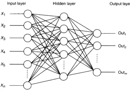
Referring to Figures 1-2 and 1-3, this simplified model of the real neurons contains a set of input connections that brings in signals from other neurons, a synapse that connects neurons of different layers and a weight unit for each synapse. The summing
X1 X2 Out, X3 Out2 X4 X5 Outm Xn
Figure 1-2: A three layer network: stimulation is applied to the inputs of the first layer, and signals propagate through the hidden layer to the output layer. Each connection between neurons has a unique weighting value.
xl
x,
YX IW . Summing Junction Xn Wn Input Synaptic Signals Weights Yk Output Activation Signal FunctionFigure 1-3: Artificial Model of Neuron
junction integrates the inputs and then applies a non-linear activation (thresholding) function to make an output decision. The output of the activation function is then broadcasted to some or all of the neurons in the subsequent layers. In order to use the network, we apply the input values to the inputs of the first layer, allow the signals
25
to propagate through the hidden layers of the network and read the output values at the output layer.
Fig-1-3 represents the mathematical model of a neuron. Signals enter the synapse on the left, are either enhanced or diminished depending on the weights associated with the synapse and are then summed in the neuron. The neuron then applies a simple activation function (f(.)) to the sum and outputs (Yk) the result of which propagates to further neurons via other synapse. The operation of this simple neuron can be modeled as follows in the following equation:
k
y(x, w) =
f(Z
xii) (1.1)where xi and wi are the inputs and the weights respectively, and f(.) is the thresh-olding function of the neuron.
1.1.2
Learning in ANNs and Training Algorithms
Artificial Neural Networks (ANNs) learn through training. The real intelligence of the networks exist in the values of the weights between neurons. Learning in biological systems involves adjustments to the synaptic connections (weights) that exist between neurons. Similarly, we need a method of adjusting the weights between neurons in artificial neural networks to solve a particular task. One of the most commonly used weight adaptation algorithms for multilayer perceptron neural network (MLPNN) is known as the back propagation algorithm (BPA). BPA is a learning procedure for networks of neuron-like units by repeatedly adjusting the weights of the connections in the network to minimize the difference between the actual output of the network and the desired output vector[16]. BPA is the best example of a parametric method for training supervised multi-layer perceptron (MLP) neural network for classifica-tion and pattern recogniclassifica-tion [6], [7], [50]. BPA, like other supervised multi-layer feed
forward neural network training algorithms has the ability to learn weights and input biases.
BPA uses gradient descent to iteratively minimize the gradient of the error func-tion. It always shows the direction of the steepest ascent of the error funcfunc-tion. There-fore, we can start with a random weight vector and follow the negative gradient with some learning rate q.
Wt+i = Wt + 6
Wt, = - Eww (1.2)
It should be noted that this will only find the local minimum. Therefore, the gradient descent procedure should be repeated for several random initial states. Gradient descent based BPA is a powerful method to manage systems that use data to adjust the network weights and thresholds for minimizing the errors in its prediction on the training data set. In Simpkins's[56] work a gradient descent algorithm was used to train a five layer COIN co-processor.
1.2
The COIN Co-Processor and Hardware
Imple-mentation of Artificial Neural Networks
There are some direct analogies between biological neural systems and analog neural processors. This includes amplification, exponentiation, thresholding, compression and integration. The parallels between these two worlds run from the level of device physics to circuit architecture. Artificial analog neurons are realized through analog components like adders, multipliers, current to voltage converters, memory circuits and thresholding elements.
In the last few decades, most efforts to develop ANN's have focused on the area of mathematical considerations and are mainly implemented in software [29]. How-ever, in recent years researchers have made efforts to create neuro-inspired processor chips to process information in hardware. One of such processors include the recent state-of-the-art IBM's custom made "brain-like" chip called TrueNorth. TrueNorth
comes packed with 256 million neurosynaptic cores, 64 billion neurons and 16 Trillion synapse [47]. One of the reasons for the growing interest in hardware based ANN's is because they can be faster compared to the software ones when very large number of interconnections are required as in the case of the IBM TrueNorth.
Most hardware implementation of neural networks is based on very large scale integration (VLSI) technology which is functionally highly versatile but mostly limited to two dimensions. Although the planar nature of VLSI is not necessarily a restriction for neural implementations but the lack of of a third dimension limits the number of synaptic densities that can be accomplished due to interconnection delays and packaging of input/output pins [65], [68]. The use of optical techniques to implement interconnections in neural network systems appears to be a very attractive approach
[1],[17],[21]. Moreover, the dynamic modification of interconnections as required by
the training algorithm is difficult to implement electrically. The key advantages over electronic interconnections are the massive parallelism [41], speed and cross-talk free interconnections.
Hybrid opto-electronic neural systems such as the COIN processor combine the technological advantage of both domains, with functionally rich local electrical pro-cessing and global optical interconnects. With optical signals as inputs, COIN per-forms the required computation using electronic circuits and the processed result is presented as another optical signal which can be interconnected optically through free space or optical elements to subsequent processing units. Because optical signals do not interfere with each other in the same way as electrical signals, we can accomplish parallel computation and eliminate interconnection delays and I/O issues [19], [27],
[28]. Consequently, the performance of an integrated processor is greatly enhanced.
Thus, optics is well suited for this kind of system because the interconnections can be implemented via the third plane by utilizing the parallelism of optical signals [26],
[27].
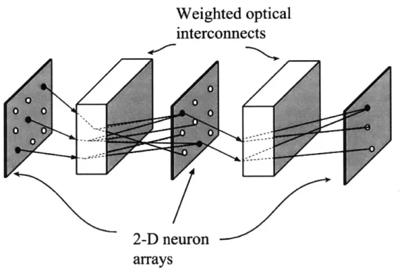
A schematic of a three layer optoelectronic neural network architecture is given
in Fig. 1-4. The neurons are arranged as 2-dimensional arrays and each array
sponds to one neuron layer in the network. Although there is always one input layer and one output layer, the number of hidden layers can be changed depending on the complexity of the task. Since the interconnections between different neuron layers are implemented by optical signals, each pixel must be able to detect incoming optical signals and produce optical outputs. As a result, each neuron is generally comprised of three components: optical receivers (i.e. photodetectors), non-linear electronic el-ements (activation functions) and optical output transmitters (e.g OLED). The most commonly used activation function in neural networks is the sigmoid thresholding function. Other types of neuron activation functions include the tanh function, the saturated linear function, etc. A description of different types of activation functions and their performance metrics will be discussed in detail in chapter-3.
Weighted optical
interconnects
0 0 0 02-D neuron
arrays
Figure 1-4: Schematic architecture of a multilayer optical neural network. Each circle represents a neuron while a filled circle means that the neuron is in the "ON" state
Input signals detected by the optical receivers are mapped to the optical output
29
transmitters through the non-linear electronic elements as:
N
yj = Gf(E wixi)) (1.3)
i=1
where yj is the optical output from the jth neuron in the current layer, G is the opto-electronic gain, f(.) is the non-linear neuron response function, N is the total number of input neuron in the previous layer, wij represents the interconnection weight be-tween the two neuron layers, xi is the input from ith neuron ion the previous layer.
A neural network can be trained to solve a specific task by adjusting the
interconnec-tion weights using an algorithm such as the gradient descent learning algorithm[3]. In addition to the easy implementation of optical I/O's and the benefits of densely packed interconnections, an optical neural network can also be used to implement the weights in the form of holographic memory [11], [31], [32]. Furthermore, the inter-connection weights can be adjusted in real-time using dynamic holograms recorded in photo-refractive crystals. Therefore, the training of an optical neural network can be done relatively easily by updating the weight according to the comparison result between the output of the neural net and the desired response.
1.3
Thesis Summary
The remainder of this thesis consists of three parts encompassing the body of the work completed as part of the development process of the COIN Co-processor. Chapter 2 provides background information on COIN system. Furthermore, previous work regarding the circuit implementations of activation functions are discussed. In chapter
3, the detailed mathematical models of different types of neural activation functions
and their performance metrics will be explored.
Next, the major contribution of this thesis is presented in chapters 4 and chap-ter 5. Three versions of the optoelectronic thresholding function will be explored in these chapters. The first version used the original COIN processor model to come up with a memory-less, fixed weighting and fixed thresholding circuits to perform
optoelectronic thresholding of the input optical signal. The original COIN proces-sor used spatial light modulators (SLMs) to adjust the weights between neurons. Version-II and version-III focus on the most recent development of the COIN Co-processor architecture and will have both analog weighting and memory elements. The integration of the weighting circuits into the thresholding circuits eliminates the presence of the bulky SLMs in between neuron layers. Version-III is different from version-II because of the additional flexibility in changing the thresholding voltage of the activation function by applying different bias voltages to shift the turn on points. Furthermore, version-III requires IC implementation since some of the tran-sistors need to be operated in sub-threshold regimes. Version-III is based on the optoelectronic implementations of the hyperbolic tangent functions in analog CMOS circuits.
Finally, chapter 6 presents the conclusions, the applications of ANNs (particularly the COIN processor) and future plans.
Chapter 2
The COIN System
In this chapter, a description of the COIN Co-processor and the major components that makeup the architecture of the system will be discussed thoroughly. Furthermore, previous work on hardware, particularly, mixed-signal and optoelectronic circuit im-plementations of the thresholding functions will be presented.
2.1
Background on Compact Optoelectronic
Inte-grated Neural (COIN) Co-processor
The work presented in this thesis is part of the development of the COIN Co-processor in the Photonics Systems lab at MIT. The COIN Co-processor is a pixellated, rugged, parallel, feed-forward and integrated optoelectronic implementation of an artificial neural processor. The basic architecture of the COIN co-processor is shown in Fig.
2-1 consists of 3 layers each of which contains an array of N-by-N pixels. Information
enters optically through one end of the device, propagates through several layers of individual processing elements, and exits the opposite end of the device. Each layer consists of 2-D arrays of photodetectors which do summation of the input light sig-nals, threshold electronics which perform thresholding, optical interconnect elements which steer optical signals between layers, and a controller which supervises the sys-tem. These layers of networks are cascaded to form a multi-layer processor and in the
work of
[1]
a five layer network was implemented and trained. The full embodiment of this system would allow computers to solve a new class of problems and complex functions such as pattern recognition and approximation at a faster speed and lower power expenditure.This architecture will be slightly modified to incorporate weighting circuits and associative (local) memory elements in versions-II and III. Designs of the electronic processing circuits are discussed in chapter 5.
Light Sources
Threshold Electronics Interconnect Elements
Photodetector Array\ Spacing Plate
Input
Optical -+'
Signal
Controller
Figure 2-1: A Block Diagram of a three layer COIN Co-processor system. Adopted from the work of Travis Simpkins[ ]. Each layer consists of arrays of photodetectors, optical interconnection elements and thresholding circuits
2.2
COIN Component Considerations
In this section, the core components that are required for the realization of a single layer of the COIN co-processor will be presented. This includes a photodetector, threshold circuit. driver and weight circuits. optical output sources and optical in-terconnection elements. The pros and cons of various detectors and optical output sources (such as transmitters and emitters) are also explored briefly.
34
Optical Signal From Previous Plane of Neuron4 oto-detector- ~3 - - Optica Threshold * * * To Circuit wPlane o
Driver Circuits Sources Optical
with Weights Elements
Figure 2-2: A Diagram of a COIN neuron
2.2.1
Photodetector Considerations
The photodetector is an optical signal receiver which converts the received optical signal to an electrical signal (current or voltage). The three important performance parameters for the selection of the COIN photodetectors are high sensitivity,
linear-ity and dynamic range. The magnitude of the dynamic range which is the ratio of
the maximum and the minimum detectable power is one of the most important mea-sures of the performance of the detector. The maximum detectable power is limited
by a non-linear response (saturation in this case) whereas the mlinimuin detectable
power is determined by the noise level of the photodetector. Furthermore, the pho-todetector should exhibit high linearity over a wide range of dynamic range. The linearity is extremely important because it determines the niaxilmim amount of light intensity that can be collected and summed without saturating the phototransistor. High responsivity and high quantum efficiency with minimum equivalent noise are also relevant. Quantum photodetection can be accomplished by using photodiodes, phototransistors or photoresistors
[
], [u],
[
,[
'1.Photodiodes are sericonductor devices with a p-n junction or p-i-n structure and
35
I
I Signal Next f Neurons Phthey generate a photocurrent by absorbing light in a depletion region[
],
[
].
Photo-diodes are very compact, fast, highly linear and exhibit high quantum efficiency (i.e generates nearly one electron per incident photon [- ] [ -]) and high dynamic rangeif they are operated in combination with suitable electronics. The ideal photodiode can be modeled as a current source in parallel with a semiconductor diode. The cur-rent source corresponds to the curcur-rent flow caused by the light-generated drift curcur-rent whereas the diode corresponds to the behavior of the photodiode junction in the ab-sence of incident light. An actual photodiode will have a junction capacitance (Ci)
that is generated due to the depletion layer that exists between the two conductive layers and a finite shunt resistance (RsH)
K
as shown in Fig. 2-3. A photodiode actsPndet light
IC'
diodeFigure 2-3: Lump-sum equivalent-circuit model of a photodiode
like a photo-controlled current source in parallel with a seniconductor diode and is governed by the standard diode equation.
q "D
I = photo - Idk (e kT _ 1) (2.1)
where I is the device current, 'photo is the photo-generated current, Idk is the dark or the "non-light" reverse current, VD is the forward bias voltage, q is charge of an electron, k is Boltzmann's constant and T is the temperature in degrees Kelvin. The photocurrent can be amplified and fed into a readout device. Idk is the diode's reverse leakage current and flows even in the absence of incident light. As we see from the standard diode equation, this dark current increases with increasing reverse voltage
(VD) bias and temperature. It approximately doubles every 100C
[ ], [
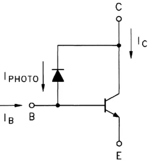
].Phototransistors are photodiode-amplifier combinations integrated within a single silicon chip which exhibit more sensitivity compared to photodiodes. These combina-tions are designed to overcome a major limitacombina-tions of photodiodes: unity gain. The
C
IC
P HOTO
E
Figure 2-4: Phototransistor Equivalent Circuit
phototransistor can be viewed as a photodiode whose output current is fed into the base of a conventional signal transistor as depicted in Fig. 2-4. Based on this model of the phototransistor it displays some of the characteristics of both types of devices. The typical gain of a phototransistor can range from 100 - 100000[60]. The structure
of phototransistor is very similar to that of a photodiode. In fact, the collector-base junction of the phototransistor can be used as a photodiode with fairly good results. The major structural difference is that the phototransistor has two junctions com-pared with one for the photodiode.
Photoresistors which are based on certain types of semiconductors can also be used as photodetectors[46]. They are cheaper than photodiodes but they are slow, less sensitive and exhibit a strongly non-linear response. The photoresistivity of photoresistors is highly sensitive to temperature and thus they are unsuitable for applications requiring precise measurement of sensitivity to light[4].
2.2.2
The Threshold Circuit
Optical networks always require a non-linear functions that are difficult to implement optically. As a result, optical neural networks leave this non-linear function to be implemented electronically. The use of optoelectronic circuits provide the flexibility of implementing complex neuron response functions and of fine tuning the properties of the neurons as is required by the neural network algorithm that is being imple-mented. The threshold circuit is a light in-light out device that performs intensity thresholding. Based on the sum of the input intensities from nine neighboring pre-vious layer nodes, it decides whether to generate a high or a low output intensity. Each neuron in array would receive signals from previous layer neighboring arrays, compute a non-linear function based on these input values and transmit signals to next layer neuron arrays. The threshold circuit is analogous to the squashing func-tion in artificial intelligence(AI). However, the threshold circuit in this case employs optoelectronic circuit devices as opposed to software algorithms to accomplish light intensity summation and output decisions.
2.2.3
Driver circuits and weight storage elements
The driver circuits are often used to regulate the current flowing through the output light sources and can easily be accomplished with a simple MOS resistor. The weights are stored in a short term analog memory such as capacitors. These weights are uploaded to the gates of driver circuits periodically during the learning process to regulate the relative output intensity of the synapse circuits.
2.2.4
Output Light Sources
The output light sources act as the interface between the electronic domain and the optical domain of the COIN Co-processor. The ultimate goal of the COIN project is to develop a compact and integrated optoelectronic neural processors. Thus, the optical output light sources are extremely important in determining the transmission efficiency and the size of the system. There are a few candidate optical transmitters for
the integrated optoelectronic neural networks. These include semiconductor LEDs, laser LEDs, optical modulators and Organic LEDs (OLEDs).
The Light Emitting Diode (LED)
The light emitting diode (LED) possesses a p-n junction which emits light when a for-ward bias voltage is applied. Electrons in the donor level below the conduction band of the junction move to the acceptor level above the valence band and lose energy in the process. This energy is emitted as radiant energy in the infrared or the visible region. LEDs are commonly made of GaAs doped with one or more impurities. They are relatively easier to integrate into a chip compared to optical modulators. Fur-thermore, the internal quantum efficiency of a double hetrojunction semiconductor
LED can be very close to 100%[54]. However, the fact that LED's emit light in all
direction makes it very difficult to collect the optical output. Consequently, LED's generally suffer from low external efficiency. As a result, higher driving current is needed which results in higher power consumption. Furthermore, since the output of the LED comes from spontaneous emission, it has a wide-band spectrum and is therefore temporally incoherent. This incoherence makes the recording of holographic interconnections impossible [48] and limits the application of LED-based neuron ar-rays to non-adaptive systems.
Organic LED(OLED)
OLED which stands for organic light-emitting diode is made with organic compound
that lights up when a voltage greater than the minimum turn-on voltage is applied across the two terminals. Although LEDs have high optical output and a wide band-width in the order of MHz, the production is expensive compared to OLEDs. One of the major advantages of OLEDS compared to LEDs is that a large area of its arrays can be produced at lower cost. Compared to incandescent and fluorescent light sources, white OLEDs can emit light that is brighter, more uniform with higher power efficiency[33]. Furthermore, OLEDs can be made to be extremely small, thin, flexible and most importantly can be spun on to a chip on a wafer. The MEng thesis
work of [51] explored the applications of OLEDs for COIN system and compared its performance to Vertical Cavity Surface Emitting Lasers(VCSELS). The work of [51] and others indicate that OLEDs have the potential to emerge as alternative light sources for integrated optoelectronic neural processors.
Diode Lasers
Laser diodes are the other candidates for on chip output light sources. Its bandwidth is much narrower compared to LED's and therefore has high degree of coherence. The light is emitted in one direction and therefore has very high efficiency. However, laser diodes require more complicated material preparation and processing techniques[37]. In addition to that, lasers have a threshold input power before coherent light is emitted, and therefore will have a higher power consumption per neuron than LEDs.
Optical modulators
Optical modulators are also possible alternatives for output light sources. The op-toelectronic gain can be increased easily by increasing the power level of the laser source without affecting the power consumption of the neuron chip. As a result, we can build arrays with high density due to the lower consumption of modulator based neuron light sources. By using single laser as the off-chip light source, we can achieve both temporal and spatial coherence which is required for the effective implementa-tion of the holographic interconnecimplementa-tions in adaptive neural networks[57]. However, the alignment of the optical system is more complicated due to the addition of off-chip light sources.
2.2.5
Optical Interconnects for COIN
The optical interconnection element provides a free space communication between dif-ferent layers of neurons. It directs the output of a synapse to the correct set of neurons in the subsequent layer. Bill Herrington's PhD work[23] focused on developing this medium for the COIN Co-processor.
2.3
Previous Work on Neural Activation Functions
and Weighting Circuits
Various efforts were made previously to create neuro-inspired local (associative) mem-ory elements and activation circuits in both optics and electronics domains[18]. For many reasons that were discussed in the previous chapter most optical weighting and thresholding implementations were found to be bulky and non-adaptive for hardware based neural networks. Consequently, the majority of the discussion on previous work will be focused on optoelectronic implementations of local memory and activa-tion funcactiva-tions in digital, analog or a combinaactiva-tion of both domains along with optical emitters and receivers.
2.3.1
Optoelectronic Neuron Circuit with Variable Synaptic
Weights
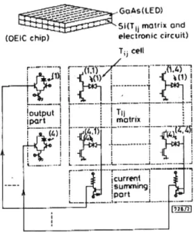
In this journal letter[66], a basic optoelectronic circuit of artificial neuron was realized
by controlling the synaptic weights electronically. An addressable memory unit was
constructed using an optical interconnection element between the emitters and the detectors. The basic neuron circuit in this work consists of three parts which are the Ti cells, a current summing node and an output node, as shown in Fig.2-6. The Tj cell acts as the synaptic connection and connection weights and polarity are controlled
by the gate voltages Vgi and Vg2 of NMOS FETs of Q1 and Q2. For excitatory neural
connection V1 is high and V2 is low; thus Q1 is "on" and Q2 is "off'. For inhibitory
neural connections, Vi is low and Vg2 is high; thus Q1 is "on" and Q2 is "on". When both Vgi and Vg2 are low no connection is formed and thus both Q1 and Q2 are "off'. Furthermore, the artificial neuron could have many Tij cells like the human brain collecting signals broadcasted from neighboring synapses.
The photocurrent Iij is generated using a bidirectional photodiode(PD) when the optical outputs from other neurons are received. The photocurrent flows from Q1 to PD in the excitatory connection and from PD to Q2 in the inhibitory connection. The
/curenl '
(1 cell) %urnming fDutput \
port \port / LE 0 1 2 ,-e- Mtl Dry /1C. connlfl o 0 TV,92-0) g ot Q Votage V 1 and Vg2. V -50l Cl~t ion 6191 _0)
Figure 2-5: Optoelectronic neuron circuit and synaptic connection (Tij cell). a) Basic neuron circuit. Photocurrent Iij flows from MOSFET Q1 to PD for excitatory con-nection, and flows in inverse direction for inhibitory connection. b) Photo-currents for excitatory and inhibitory connections. Bipolar Tih values were obtained by following
combination. Adapted from
[
]V V
1 5 0 0 0 0
-1 0 5
Figure 2-6:
photocurrents from neighboring Tij cells were summed in the current summing potion of the circuit. When the summed result is above the threshold value, the GaAs LED located in the output circuitry emitted optical light to the other neurons. When the summed value is less than the threshold value, no optical output light was emitted to other neurons. Finally, a 4x4 array with a content addressable memory(CAM) was implemented as a proof of concept for a large scale optoelectronic network as shown in Fig. 2-7.
GoAs(LED) Si(T11 mOtrix and
(QEIC chip) electronic circuit)
T cell !output T11 igart matrix I icurrenit sumnming Port
Figure 2-7: Primitive optoelectronic CAM circuit with 4 x 4 network. Adapted from
[F ]
2.3.2
Digital-Analog Hybrid Synapse Chips for Electronic
Neural Networks
In this work [''-], a 32X32 programmable array of synapse chip was fabricated for par-allel implementation of neural networks. The synapses are based on a hybrid digital-analog design which utilized on-chip 7-bit data latches to store quantized weights and a two quadrant multiplier DAC's to compute weighted outputs. As depicted in the block diagram given in Fig. 2-8, the chip consists of an address/data de-multiplexer, row and column address decoders, 64 analog input/output lines and 1024 cells ar-ranged in the form of a 32x32 cross-bar matrix.
A circuit diagram of the 7-bit DAC is shown in Fig.2-9. The DAC consists of a
current input circuit, a set of binary weighted current sources and a current steering circuit. The current in the input circuit is mirrored by the binary-weighted current sources for all synapses along the column. Two versions of the chip were fabricated. In one version, a single long-channel FET was used to convert the synapse input voltage into current. In the second version, an external resistor was employed to perform input voltage to current conversion when high linearity was required. The
Figure 2-8: Simplified block diagram of hybrid 32x32x7-bit synapse chip. Adapted from [ ]
responses of both versions of the chips are shown in Fig. 2-10
Figure 2-9: Block diagram of 7-bit multiplying DAC. Adapted from [ ]1.
In this chip, two optimization problems, namely, the one-to-one assignment prob-lem and the traveling salesman probprob-lem were impprob-lemented. In order to test the performance of the network for speed and quality, a 64-neuron breadboard system used along with operational amplifiers operating as a current summing amplifier as depicted in Fig. 2-11.
One of the biggest problems related to this architecture in addition to reduced network density and lower speed is the stability issue associated with the
(b)
100
0
1 - 1- -_
2 4 6 8 10
VOLTAGE INPUT (volts)
(a)
CII-I.
U E DV
15 5 0 2 4 6 8 10VOLTACE INPUT (volts)
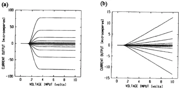
Figure 2-10: Transfer characteristics of a 7-bit synapse for weight values of 0 +/-1, 3, 7, 15, 31, 63 (a) with long channel transistors and (b) with external 10MQ for voltage to current conversion. Adapted from
[.
V.. 1- 1 Vi 1
Figure 2-11: Electronic circuit neuron model and synapses. Where V4 is of the neuron i, Tj is the synaptic weight from neuron
j
to neuron i, Rfthe output and Cf are the feedback capacitance and resistance of the neuron, and I is the external input current. RF and Cf should be chosen to ensure stability against oscillations. Adapted
from [].
tional amplifier. As a result, this architecture is not a viable choice for processor architectures such as COIN. Other previous related work includes Travis's electronic thresholding circuit[
cial vision systems[
] and a comparator based activation circuit designed for
artifi-45 100
I
aI
rLAJ 50 F-a -SDF I .. 0 C RF VjChapter 3
Mathematical Models of Different
Types of Activation functions
1
The objective of this chapter is to develop the mathematical models of neural activation functions needed to accomplish bistability in neural networks. Artificial neural networks have developed rapidly in the past few decades both in theory and in hardware implementations. Developing the mathematics behind will give us a flexibility in designing and implementing the various types of neural activation func-tions in optoelectronic hardware. Activation funcfunc-tions of neural networking can be continuous, i.e sigmoidal functions, piece-wise linear or isosceles triangular functions. Continuous functions are the preferred squashing functions for neural networks for their non-linearity and the requirement of derivative based parameter methods such as back-propagation [9]. One example of thresholding functions is the well known sigmoidal function. Sigmoidal output functions are good squashing functions for un-bounded activation[15]. Other examples include the hyperbolic tangent function and the arc-tangent function which can be used to accomplish both positive and negative unbounded activation.
'Thresholding function is also known as the activation function, squashing function or weighting function. In some literature, it is also called the neural transfer function. They all refer to the same term and can be used interchangeably in this thesis.

![Figure 2-8: Simplified block diagram of hybrid 32x32x7-bit synapse chip. Adapted from [ ]](https://thumb-eu.123doks.com/thumbv2/123doknet/14687879.560586/45.918.240.655.131.359/figure-simplified-block-diagram-hybrid-synapse-chip-adapted.webp)