Demonstration System for a Low-Power Seismic
Detector and Classifier
by
Elliot Richard Ranger
Submitted to the Department of Electrical Engineering and Computer
Science
in partial fulfillment of the requirements for the degree of
Master of Science in Electrical Engineering
at the
MASSACHUSETTS INSTITUTE OF TECHNOLOGY
June 2003
c
E. Ranger, 2003. All rights reserved.
The author hereby grants to MIT permission to reproduce and
distribute publicly paper and electronic copies of this thesis document
in whole or in part.
Author . . . .
Department of Electrical Engineering and Computer Science
May 9, 2003
Certified by . . . .
Thomas F. Knight, Jr.
Senior Research Scientist, MIT
Thesis Supervisor
Certified by . . . .
Kenneth M. Houston
Group Leader - Analog Systems, C.S. Draper Laboratory
Thesis Supervisor
Accepted by . . . .
Arthur C. Smith
Chairman, Department Committee on Graduate Students
Demonstration System for a Low-Power Seismic Detector
and Classifier
by
Elliot Richard Ranger
Submitted to the Department of Electrical Engineering and Computer Science
on May 9, 2003, in partial fulfillment of the
requirements for the degree of
Master of Science in Electrical Engineering
Abstract
A low-power seismic detector and classifier was designed and implemented which was
able to detect the footsteps of a person from as far as 35 meters away.
Through-out the design an emphasis was placed on using low power circuitry and efficient
algorithms. The test platform to demonstrate the concepts of the design utilizes
a revolutionary low-power microcontroller and Digital Signal Processor (DSP) from
Texas Instruments, Inc.. The DSP is a fixed-point processor that is underclocked to
minimize power consumption and the microcontroller has idle modes which consume
microamps of power. The system is designed to run on battery power, and uses solar
power to continually charge the batteries during the day. Lastly, a “Commercial Off
the Shelf” RF module allows multiple sensors to communicate with themselves to
triangulate position, or to relay detections and commands to and from a base station.
Thesis Supervisor: Thomas F. Knight, Jr.
Title: Senior Research Scientist, MIT
Thesis Supervisor: Kenneth M. Houston
Acknowledgment
May 9, 2003
This thesis was prepared at The Charles Stark Draper Laboratory, Inc., under Internal
Company Sponsored Research Project IRD03-2-5042.
Publication of this thesis does not constitute approval by Draper or the sponsoring
agency of the findings or conclusions contained herein. It is published for the exchange
and stimulation of ideas.
I always enjoy reading the acknowledgment section of my fellow colleagues’ thesis
documents. It is the one section of the report where you get to take a glimpse into
the author’s life and learn about the people who influenced them. Sir Isaac Newton
once said, “If I have seen further [than others] it is by standing on the shoulders of
giants”. I prefer to take a more humble approach and say it is because I have had
the shoulders of the great people who have helped me that I have seen so far.
My family has always been a source of strength and nourishment. Lots of things
come and go in your life: you change careers, where you live, and what walk of life
you choose to pursue. One thing that has always remained a constant in my life has
been my family. They have inspired me with their continual support to always reach
for the stars. I owe them a deep sense of gratitude for making education such a high
priority.
Thomas Knight and Kenneth Houston, my two advisors, helped me solidify my
project, come up with the resources to execute the project, and gave me the confidence
that I was doing a notable job. We have had some interesting experiences together
from lunches at the Cambridge Brewing Company to exhaustive days of testing in
the park. Without the support of these two, this project would never have occurred
or have been completed.
I owe a special recognition to the guys at Draper who helped me throughout my
stay there: Jack McKenna, Mike Matranga, Jim Scholten, Dan McGaffigan, Charles
Barone, Bob Menyhert, Bill Russo, Dennis Kessler and Fred Kasparian. Some of the
guys I talked to about the technical aspects of the project and other guys I talked to
about the stock market or politics, but I value the assistance all of them provided.
One person who deserves a little more thanks is my officemate Sermed Ashkouri. He
got to put up with all the daily joys of having me in the same office.
Lastly, there are numerous friends and colleagues along the way that have provided
me with a spring-board to bounce ideas off of. Although there is not room to mention
all of you rest assured that the thanks is still forthcoming.
Contents
1
Introduction
17
1.1
Background . . . .
18
1.2
Previous Work
. . . .
19
1.3
Research . . . .
19
1.4
Overview . . . .
23
2
System Architecture
25
2.1
Digital Signal Processing . . . .
27
2.1.1
Bandpass Filter . . . .
28
2.1.2
Envelope Detect . . . .
29
2.1.3
Decimation . . . .
29
2.1.4
Hanning Window . . . .
31
2.1.5
Fast Fourier Transform . . . .
31
2.1.6
Spectral Normalization . . . .
33
2.2
Footstep Detection Algorithm . . . .
34
3
Design Description
37
3.1
Analog Design . . . .
38
3.1.1
Geophone . . . .
38
3.1.2
Filtering . . . .
39
3.1.3
Amplification . . . .
41
3.2
Digital Design . . . .
41
3.2.1
MSP430F149 Microcontroller
. . . .
41
3.2.2
TMS320VC5509 Digital Signal Processor . . . .
48
3.2.3
Host Port Interface . . . .
51
3.3
RF Design . . . .
52
3.4
Power Design . . . .
52
3.4.1
Solar Power . . . .
53
3.4.2
Battery Charger . . . .
54
3.4.3
External Power . . . .
54
4
Test Procedure
55
4.1
Unit Level Testing
. . . .
55
4.2
System Testing . . . .
56
4.2.1
Data Collection . . . .
56
5
Results
59
5.1
Detection Performance . . . .
59
5.2
Analog Performance
. . . .
64
5.3
Solar Power . . . .
67
5.4
Power Usage . . . .
67
5.5
RF Range . . . .
67
6
Conclusion
69
6.1
Future Enhancements . . . .
71
6.1.1
Algorithm Improvement . . . .
71
6.1.2
DSP Technology
. . . .
72
A Schematics
73
B Parts Listing
79
C Assembly Drawing
83
D Test Procedure
85
E TMS320VC5509 Source Code
93
E.1 bootcode.asm . . . .
93
E.2 define.h
. . . .
98
E.3 difference.asm . . . .
99
E.4 extern.h . . . .
100
E.5 filters.h . . . .
101
E.6 firdecimate.asm . . . .
103
E.7 hanning.h . . . .
106
E.8 hp filter.asm . . . .
130
E.9 hpi.c . . . .
131
E.10 include.h . . . .
135
E.11 init sys.c . . . .
135
E.12 lp filter.asm . . . .
138
E.13 main.c . . . .
140
E.14 normalization.h . . . .
141
E.15 proc cmd.c . . . .
141
E.16 prototype.h . . . .
143
E.17 signal proc.c . . . .
144
E.18 timer.c . . . .
155
E.19 variables.h . . . .
158
E.20 vc5509.h . . . .
158
E.21 vectors.asm . . . .
162
E.22 wbuffer.asm . . . .
164
E.23 window.asm . . . .
166
F MSP430F149 Source Code
169
F.1 boot dsp.c . . . .
169
F.2 comms.c . . . .
172
F.3 define.h
. . . .
175
F.4 display.c . . . .
177
F.5 extern.h . . . .
180
F.6 flash.c . . . .
180
F.7 hpi.c . . . .
182
F.8 include.h . . . .
191
F.9 init sys.h . . . .
191
F.10 low power.s43 . . . .
198
F.11 main.c . . . .
198
F.12 menu.c . . . .
199
F.13 proc adc.c . . . .
204
F.14 proc cmd.c . . . .
209
F.15 prototype.h . . . .
218
F.16 signal proc.c . . . .
219
F.17 timer.c . . . .
222
F.18 typedef.h . . . .
223
F.19 variables.h . . . .
225
G Errata
227
List of Figures
1-1
Solar Isolation (kW h/m
2/day) in the U.S. . . .
21
2-1
Signal Processing Path . . . .
26
2-2
Signal After Bandpass Filter . . . .
30
2-3
Envelope Detection . . . .
30
2-4
Decimation
. . . .
31
2-5
Hanning Window . . . .
32
2-6
Hanning Window Applied to Footstep Data
. . . .
32
2-7
Scaled FFT Output . . . .
33
3-1
Analog Frontend Stages
. . . .
38
3-2
Bode Plot for Analog Frontend
. . . .
40
3-3
Main Menu . . . .
44
3-4
VC5509 Menu . . . .
44
3-5
Geophone Menu . . . .
44
3-6
ADC Menu . . . .
44
3-7
Miscellaneous Menu . . . .
45
3-8
Solar Panel
. . . .
53
4-1
Footstep Data Collection Setup . . . .
57
5-1
Magnitude, Phase and Noise Plots for Board SN101 . . . .
65
5-2
Magnitude, Phase and Noise Plots for Board SN102 . . . .
66
List of Tables
3.1
Microcontroller Memory Map . . . .
42
3.2
Initial Configuration of Port Registers . . . .
46
3.3
DSP Memory Map . . . .
49
3.4
HPI Write Memory Map for Saving Program Code
. . . .
50
3.5
HPI Command Codes . . . .
51
5.1
Detection Data . . . .
63
5.2
Subject Data
. . . .
64
Chapter 1
Introduction
Recently, there has been a great emphasis on low power circuit design. This has
revo-lutionized many areas in computers and electronics. One area specifically benefitting
from the improvements in lower power consumption is sensors. Sensors can now run
for weeks with the power of only a couple Lithium Ion batteries. This means they
are cheaper to operate, and more importantly, they require less human intervention
because the operator does not have to replace the batteries as frequently. Texas
In-struments, Inc., has an Ultra-Low-Power Microcontroller which only draws 2.5 uA
of power in certain operating modes [13]. New advances in programmable parts are
being made as well. Combining this low power mentality in an area which has not
had much research is the goal of this thesis.
When a person or animal walks along the ground they emit seismic waves as a
result of the impact. These waves then propagate through the ground. A geophone is
a sensor that is able to measure the amplitude of these seismic waves in the ground.
geophones can be used to measure everything from a car driving by to an outright
earthquake. The critical part is then establishing algorithms that allow the device to
differentiate seismic waves coming from a person versus other seismic activity.
This project is an improvement to current technology in a number of regards.
First, it will focus on low power components. Next, it focuses on the development of
simple yet effective algorithms to detect and classify people. Numerous algorithms
exist for classifying data, however, most of them are not intended for low power
applications. The algorithms utilized for this project will need to be relatively simple
so they can run in a low power environment, but also still need to maintain their
effectiveness in classifying people. Lastly, is the consideration of alternative forms of
energy. This area is frequently overlooked when designing systems, but will no doubt
become more important in future designs with our diminishing supply of natural
resources. Combining all these areas in a working prototype will help advance sensor
technology as well as general design principles.
The methodology behind the design of this system was to create a platform that
later could be built upon and expanded. The scope of the project is quite expansive
and some areas have had more attention than others. Every attempt has been made
to clearly document all the aspects of the project so that in the event that someone
chooses to pursue an aspect of the project at a later point the design and results will
be at their disposal.
1.1
Background
The ground, like any other elastic medium, allows waves to propagate through it. The
impact from a footstep hitting the ground can be distinguished from as far as 100
meters away under ideal conditions [12]. The maximum distance is directly related
to the attenuation rate of the ground and the type of wave being studied. There
are four types of seismic waves that propagate through the ground: compression,
shear, Rayleigh, and Love. These waves have varying diminishing amplitudes as they
travel through the ground. The Rayleigh wave diminishes as 1/R while the shear and
compressional waves diminish as 1/R
2[11]. The Love wave, which is caused by the
layering of the soil, is not really considered. In footstep detection, the most important
wave is the Rayleigh wave. It is a wave which travels along the surface of the earth.
Its components expand in two dimensions and diminish exponentially with depth [11].
As a result of this, the wave can be detected at much further distances than the body
waves (compressional and shear). Another thing to consider is how the energy from
a footstep gets partitioned into the three waves. The shear and compressional waves
which are body waves contain roughly 26% and 7% of the energy, respectively, while
the Rayleigh wave contains 67% of the energy [11]. Therefore the Rayleigh wave is the
critical wave for footstep detection. Not only does it propagate through the ground
over greater distances, but it is also where the bulk of the energy from a footstep
gets transmitted. It is also possible to extract bearing information from the Rayleigh
wave using a three-axis geophone [11].
1.2
Previous Work
There are numerous algorithms for classifying data, however, most of them require
massive amounts of computational processing power or memory. For instance, Succi
et al, used a Levenberg-Marquardt Neural Network Classifier to track vehicle data
[10]. This produced good results, but it required 6MB of dynamic memory for its
matrix processing. In a low powered embedded system running a classifier of that
nature would require too much power.
Kenneth Houston and Dan McGaffigan at Draper Laboratory have done a
sig-nificant amount of research in the area of personnel detection using seismic sensors
[3]. Most systems prior to their work was transient based. The downfall of that
approach is that many real-world signals unrelated to human locomotion look like
transients. A systems designed like that will have either a very high false alarm rate
or else will be insensitive. They introduced the idea of using spectrum analysis on
envelope-detected seismic signals. This method not only produced reasonable
detec-tion ranges but also was significantly better at discriminating footsteps from other
types of seismic sources. This work is the basis for the algorithms that were utilized
in the system.
1.3
Research
Continuing the work on the algorithms developed by Kenneth Houston and Daniel
McGaffigan, it became desirable to examine how different geological and topological
features affected the ability to detect and classify footsteps. Also, it became desirable
to collect data from other ambulatory creatures, such as horses, to determine if there
was noticeable features which would allow the system to discriminate from horses
while still maintaining a simple algorithm.
The other area in which the project was expanded was to look at alternative forms
of energy to power the system. There are many forms of energy on the planet. Wind,
vibration, water, coal, oil, wood, nuclear fusion, and solar all produce energy that can
be transferred into electrical energy. Considering the application of this project as a
small, low-powered sensor, it is important that the energy source be able to convert
the energy into electrical energy efficiently and that the mechanism are relatively
small.
Energy can be readily converted from one form to another. However, most
tech-niques do not yield enough electrical energy to sustain a system. Amirtharajah has
proposed using ambient vibrational energy to power electrical devices [1]. Vibrational
energy does not yield enough energy to power the prototype, but solar energy is a
viable solution. Current research is around 20% efficiency which means for a 1 cm
2solar cell 20 mW of energy can be obtained [2].
Photovoltaics are materials that when sunlight hits them an electron is released
causing it to generate an electrical current. Photovoltaics are the cheapest way to
produce electricity for smaller systems and often times the simplest and cleanest to
operate. The problem with solar power is the sun is almost never directly overhead,
except in the tropics. At a latitude of 45 degrees the solar radiation may vary from
92% (early summer) to 38% (early winter) [9]. At higher latitudes the distance from
the sun to the earth becomes further and also the scattering of the sun’s radiation
from gases in the atmosphere becomes significant when considering the use of solar
power as well. Furthermore, it is important to take into account the natural landscape
such as mountains, altitude, and cloud cover. All these variables make solar power a
very inconsistent source of energy. Figure 1-1 shows some of the typical solar isolation
amounts in the United States.
Source: Sandia National Laboratories
by certain materials it can produce an electrical current. It was not until the 1950 and
the advent of solid-state devices that people were able to do something meaningful
with this information. The space program was the first application for solar cells and
in 1954 a 4% efficient silicon crystal was developed [9]. As early as 1958 a small array
of solar cells was used to provide electrical power to a U.S. satellite.
Photovoltaic cells are created by doping a material like silicon with a substance
like Boron or Phosphorus which has one less or one more electron respectively. A
junction forms between the doped silicon and the undoped silicon. When a photon
strikes the cell it contains enough energy to release the extra electron and allow it
to move across the junction. A grid is set up to gather the current from a number
of cells and different currents and voltages can be constructed depending on how the
grid is arranged.
The most common photovoltaic cell used today is the single crystal silicon cell.
The silicon is highly purified and sliced into wafers from single-crystal ingots, or grown
as thin crystalline sheets or ribbons. Polycrystalline cells are available as well but are
inherently less efficient, but they are cheaper to produce. Some of the most efficient
cells are made from Gallium arsenide; however, they are very expensive. Currently,
there has been a lot of focus on thin films made from amorphous silicon. Copper
Indium Diselenide and Cadmium Telluride may also provide viable low-cost solutions.
The thin films do not require a lot of material and have great manufacturabilty.
Another area which is receiving a lot of attention is multijunction cells. This will
allow the cell to use more of the spectrum from the sunlight giving higher efficiencies.
There are drawbacks with the use of solar energy. For one thing, it only works
when the sun is out so batteries will be required during the evening hours or if the
device is buried underground. Also, the solar cells are fragile so they will need to be
protected from adverse weather conditions.
1.4
Overview
Ultimately, the goal of the project is to produce a bread-board prototype that is able
to correctly detect and classify people. In order to accomplish this the device needs
to incorporate many types of electronics. It will require a sensor to acquire the data,
an Analog-to-Digital Converter (ADC) to convert the data to digital form, and a low
power Digital Signal Processor (DSP) to process the data. In addition, the device will
incorporate a radio frequency (RF) transmitter to relay data back to the operator
when it has detected something. Low power devices will be featured in the design,
and solar power as a means of powering the device will be explored.
Chapter 2
System Architecture
The clearest way to understand how the system processes data is to analyze it from a
signal perspective. The next couple paragraphs describe the path a signal takes from
when the sensor picks up vibrations all the way to the determination of whether or
not the signal is classified as a person.
The geophone is an external sensor with a stake on it that penetrates the ground.
It generates very small electrical voltages depending on the intensity of the
propa-gating waves in the axis that the geophone is arranged in. The geophone is biased
to fluctuate around 1.5 V, the middle of the full range input to the Analog-to-Digital
Converter (ADC). This allows use of a single supply voltage for the front-end
electron-ics and maximizes the signal voltage range. The geophone plugs into the prototype
board through port J3. The port is able to support up to there seismic channels
of data, however, currently the system is only utilizing a single channel. The other
two channels could be used to concurrently process data from two other single-axis
geophones or the data from one three-axis geophone.
When the signal arrives at the board it is initially filtered through the analog
circuitry. It is filtered through two analog lowpass filters and one highpass filter.
These filters bandlimit the signal to prevent aliasing. Then the signal goes through
a single gain stage. Following the gain stage, the signal is sampled by a 12-bit ADC
built into the microcontroller. The sampling rate is controlled by one of the internal
timers on the microcontroller and is set at 1 kHz. After eight samples have been
collected by the ADC, the microcontroller directly writes the data into a certain
memory location within the DSP through the Host Port Interface (HPI). Every 1200
samples, or 1.2 seconds at a 1 kHz sampling rate, the microcontroller takes the DSP
out of its low-power mode and requests the DSP process the next block of data.
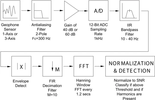
A/D
F F T
M
X
NOR MALIZAT ION
& DE T E C T ION
Geophone
Sensor
1-Axis or
3-Axis
Antialiasing
Filter
2-Pole
Fc
=300 Hz
Gain of
40 dB or
60 dB
12-Bit ADC
Sampling
Rate
1kHz
IIR
Bandpass
Filter
10 - 40 Hz
Envelope
Detect
Decimation
FIR
Filter
M=10
Hanning
Window
FFT every
1.2 secs
Normalize to SNR
Classify if above
Threshold and if
Harmonics are
Present
Figure 2-1: Signal Processing Path
Figure 2-1 shows the stages of the signal processing chain. The DSP begins by
passing the data through a digital bandpass filter allowing signals within the range
of 10 Hz to 40 Hz to pass. This bandpass range is geology dependent but was fixed
for this project. The next step is critical for the detection process. The important
part of detecting footsteps is the periodicity of the footsteps on the ground. The
time of each distinct impact on the ground is the critical information that needs to
be retained, as opposed to, the exact frequency content received at the sensor, which
can be quite variable. An absolute value is performed on the whole signal to create an
envelope of the received signal, which will peak for each distinct footstep. After this,
the data is decimated and lowpass filtered again to prevent aliasing. The decimation
occurs in two separate steps; first by 5 and then by 2. The decimation removes high
frequencies in the envelope data so as to smooth out the footstep pulses. It also allows
the Fast Fourier Transform (FFT) to be smaller to get the frequency resolution that is
required. A moving window technique employing a Hanning Window is then utilized
because the amplitude of the data is changing as the distance from the person to the
sensor changes with respect to time. Next, a 1024-point FFT is performed to convert
the data into the frequency domain. The FFT returns the values of the frequency
components as complex numbers. A function converts those real and imaginary parts
into magnitudes, and the data is scaled to make it easier to differentiate the signal
from the noise. A two-pass normalization is performed to estimate the background
level. Then the background signal (converted to decibels) is subtracted from the
seismic signal (also in decibels) so the detection is based on normalized signal levels.
Lastly, the footstep discriminator algorithm is called to decide whether the footsteps
are from a person. The details of the discriminating algorithm will be discussed later.
2.1
Digital Signal Processing
A Digital Signal Processor has specific hardware to expedite signal processing
rou-tines. It is a fixed-point processor to reduce power consumption. Using a fixed-point
processor increases the complexity of the design and requires careful design to keep
the signals scaled and in an appropriate range. Also, floating-point calculations take
many additional clock cycles on a fixed-point processor so they should be avoided.
The way numbers are represented in the processor is an important aspect of the
design stage. Using a fixed-point processor allows the programmer to pick any
arbi-trary number of bits to represent the integer portion of the number and the fractional
component. As long as the representation remains consistent the operations will
pro-duce the correct results. Texas Instruments has provided a number of common DSP
functions to assist developers using their processors. Whenever possible, these
func-tions were utilized because they are written in assembly and attempt to maximize the
efficiency of the algorithms for the hardware platform. The DSP Library functions
generally use a Q15 number representation, which means there is no integer portion,
15 bits of fractional data and one bit to represent the sign of the number.
There-fore, all the numbers represented throughout the signal processing chain are scaled
between -1 and 1.
2.1.1
Bandpass Filter
The Infinite Impulse Response (IIR) bandpass filter allows frequencies from within
the range of 10 Hz to 40 Hz to pass. Originally, it was designed to be a 4 pole filter,
2 poles for the lowpass component and 2 poles for the highpass component, however,
there were some difficulties getting the biquads to function properly. A simple 2
pole bandpass filter was resorted to, to get the system working. Within a Digital
Signal Processor the easiest way to implement an IIR filter is through the difference
equations. The single pole difference equations for the highpass and lowpass filter are
described in the equations below.
Highpass : Y
i=
N − 1
N
∗ Y
i−1+ X
i− X
i−1(2.1)
Lowpass : Y
i=
N − 1
N
∗ Y
i−1+
1
N
∗ X
i(2.2)
where N =
τ
T
, τ =
1
2π ∗ f
cutof f, T = sample period
To create the highpass filter T = 1/1000, τ = 1/(2π ∗ 10Hz), and N = 16. The
lowpass filter is realized in a similar fashion with T = 1/1000, τ = 1/(2π ∗ 40Hz),
and N = 4. This produces the following difference equations for the bandpass filter.
Highpass : Y
i=
15
Lowpass : Y
i=
3
4
Y
i−1+
1
4
X
i(2.4)
The fractional components are scaled as fractional components within the
proces-sor with 1 being represented by 32,767. Both of these filters are coded in assembly
and can be found in Appendix F in the files hp_filter.asm and lp_filter.asm.
2.1.2
Envelope Detect
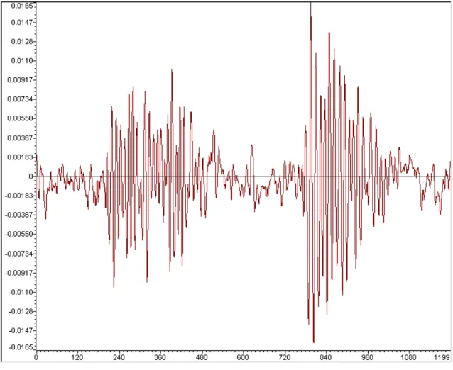
After the signal has been filtered it looks like the signal shown in Figure 2-2. Notice
how the impact from the footsteps generates both positive and negative waves. The
frequency of these waves is controlled by the terrain. The goal however is to treat
this whole block as one impact and then determine the frequency that the impacts
are occurring. In order to do this the absolute value function changes the sign of all
the negative going waves and flips them about the axis so they are positive. This
generates an envelope for each of the footsteps shown in Figure 2-3.
2.1.3
Decimation
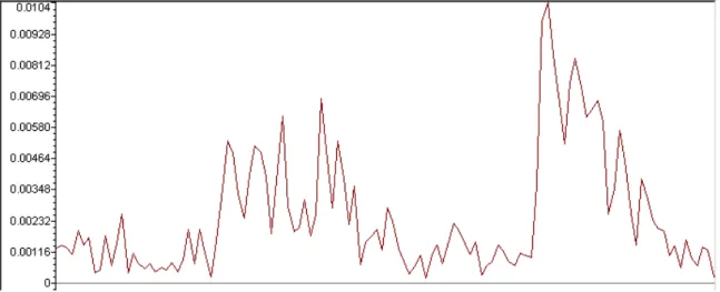
Oversampling followed by decimation has several benefits. Oversampling allows the
use of a less stringent analog antialiasing filter, which has a lower precision than a
digital filter. In addition, a digital filter does not drift with temperature or time. The
decimation stage requires a lowpass filter to prevent aliasing. The unique thing about
decimating is that the function is the same as a regular Finite Infinite Response (FIR)
filter except it is only necessary to do the operations on the values that will exist after
decimating. It is implemented in assembly as a standard FIR filter that only runs on
the samples that exist after decimating. Thus if it is decimating by two it only runs
on every other sample and if it is decimating by 5 it runs on every 5th sample. For
this application, the decimation operation is divided into two parts to limit the size
of any filter. The other benefit of decimating is it smooths out the waveform. The
same sample data after a decimation of 10 in shown in Figure 2-4.
Figure 2-2: Signal After Bandpass Filter
Figure 2-4: Decimation
2.1.4
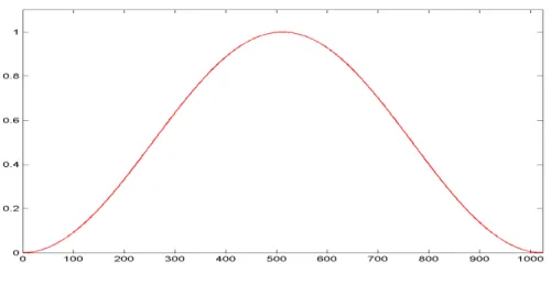
Hanning Window
Before the Hanning window is applied to the data there is a window buffer function
which takes advantage of the specialized hardware on the DSP to handle circular
buffers. A circular buffer is able to loop through the same memory space without
shifting data. It is a feature prevalent in DSPs and very handy when doing signal
processing operations. The function keeps adding new data to the end of a buffer
and outputs a linear array with the next set of data to run through the window.
The window function simply multiplies all the values in the output by the Hanning
Window coefficients. The coefficients for the Hanning Window were realized in Matlab
and a plot of the window is shown in Figure 2-5. The data after it passes through
the window is shown in Figure 2-7. The window contains about 8.5 seconds worth of
footstep data and the sampling rate is now 100 Hz after the decimation by 10.
2.1.5
Fast Fourier Transform
The Fast Fourier Transform (FFT) routine was provided by Texas Instruments in their
DSP Library. The project uses a 1024-point FFT which gives a frequency resolution
of 0.098 Hz per bin. The output from the routine segments the numbers into real
and imaginary components. The phase information is not useful for this application
Figure 2-5: Hanning Window
Figure 2-7: Scaled FFT Output
and can be disregarded. The convert_to_mag function, in Appendix F, converts
the output from the FFT to a number representing the magnitude information. It
computes the absolute value of the data, squares the real and imaginary component
and then finds the square root of the number. The square root function was provided
by Ken Turkowski [14]. The function computes the square root using only fixed-point
numbers. After the data has been converted to a magnitude, the DC frequencies
are removed from the spectrum and the data is scaled. The data after the FFT and
scaling looks like Figure 2-7.
2.1.6
Spectral Normalization
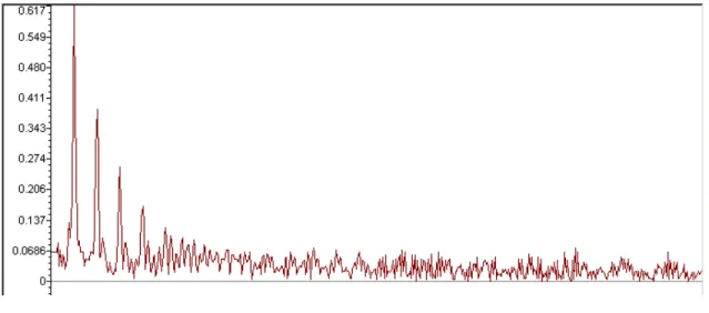
It is very clear where the first, second and third harmonics are from the FFT output
in Figure 2-7. The problem is this data are not normalized relative to the background
level. In order to normalize the data a two-pass normalization is performed on the
data. This calculates the average on both sides of a moving center point, and then
calculates the mean within the center. Ideally, the peaks in the FFT will fit into the
gap in the center. If the average of the center points divided by some threshold is
above the average of the sides then the center value gets replaced by the average from
the sides. It requires two passes because after the first pass a large peak will create
two smaller peaks in the output. The second pass helps to smooth out those smaller
peaks so that when the operation is finished there is an array which approximates
the background level of the spectrum. The width of the sides and the width of the
center section can be adjusted in the normalization.h file. Currently, the length of
the sides is 16 samples and the length of the center is 9 samples. Lastly, every point
in the output of the FFT is subtracted by the background level multiplied by two.
2.2
Footstep Detection Algorithm
The footstep detection algorithm is based on the work by Kenneth Houston and Daniel
McGaffigan [3]. Footstep data was collected from three days of testing in a few parks
around Massachusetts. The data was recorded with a 16-channel acquisition system
running into a laptop and a two channel portable DAT machine. A GPS receiver was
also carried by the individual and the data was later downloaded to a computer to
provide a ground truth. The test setup used to collect the data is described in further
detail in Chapter 4. After collecting the data, Matlab was used to post-process the
data and come up with the feature set used to distinguish footsteps.
The first criterion is that the frequency of the first harmonic for the footsteps be
in the range of 1 Hz to 3 Hz. This is the frequency range of the impacts from a
person’s feet hitting the ground. It is remarkable how periodic the footsteps of most
people are when they are walking normally. In addition to the frequency component,
the peak also has to be greater than a certain threshold relative to the noise level.
The next aspect of the detection algorithm is to verify that either a second or third
harmonic exists and that one of them is above another threshold level. The algorithm
finds the first five peaks in the range of 1 Hz to 10 Hz. Then it determines if the
peaks it acquired meet the requirement to classify it as a footstep.
The digital bandpass filter at the beginning of the signal processing chain is very
important in determining how well the algorithm performs detections and
classifica-tions. The environment and terrain can have a huge impact on the waveforms that
are observed when a person walks on the ground. In future versions one would want
to consider an adaptive bandpass filter that automatically fine-tunes the frequency of
its passband. Also, there could be intervention from the user to pick a specific land
terrain for where the sensor will be operated.
Chapter 3
Design Description
The design of the footstep detector can be broken down into four major areas: analog
design, digital design, RF design, and power design. The analog design includes all
the electronics that are necessary to filter and amplify the small voltage signal coming
from the geophone. The digital design contains the microcontroller and DSP, and all
their supporting circuitry. These chips do the analog-to-digital conversion (ADC)
and process the data to detect footsteps. The microcontroller also handles the user
interface to control various settings. The RF design is mainly an off the shelf product
which is used to allow multiple boards to communicate with each other or for the
sensor to communicate with a base-station. Lastly, the power design contains all the
circuity to support power from a battery, solar power or an external power supply.
If the system were deployed in the field the ideal solution would be to have the solar
power charge the batteries during the day and provide power for the system, and at
night power the system via battery power. Also included in the power design is the
power management scheme. Systems are shutdown when they are not in use and the
processors are put into low-power modes when they are not actively processing data.
These areas will be discussed more fully in the following sections.
3.1
Analog Design
The analog design has a separate power and ground plane from the digital area. The
geophone provides a very small voltage that varies depending on the amount of seismic
activity. This output needs to be amplified and filtered before it can be sampled by
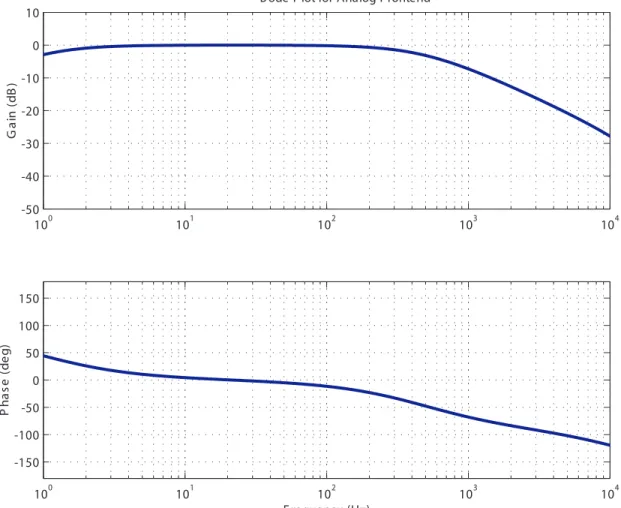
the ADC. A portion of the schematic which handles the analog frontend is provided
in Figure 3-1 for reference. The sections will be discussed later.
AGND AGND AGND GND NC COM NO I N V+ NC NC 25V 330PF 10% C79 8 4 7 6 5 U19 TL V2432 8 4 1 2 3 U19 TL V2432 GEO_A+ EJ 11 GEO_REF2 63MW 1. 0M 1% R18 7 3 2 18 6 4 5 U2 MAX4514 63MW 1. 0M 1% R17 25V 330PF 10% C78 63MW 162K 1% R16 25V 0. 1UF 10% C17 R60 1% 100 100MW R38 1% 32. 4K 63MW R37 1% 464K 63MW 63MW 100 1% R36 R35 1% 100 63MW R34 1% 31. 6K 63MW C96 10% 1UF 16V 25V 0. 1UF 10% C22 GEO_A_SEL GEO_PWR GEO_PWR GEO_A_TOUT GEO_REF2 GEO_A_OUT
GEO_A-Single-Pole RC
Lowpass Filter
Single-Pole RC
Highpass Filter
Single-Pole Active
Lowpass Filter
CMOS Switch
Determining Gain
Gain Stage
Figure 3-1: Analog Frontend Stages
3.1.1
Geophone
A geophone is a small instrument for measuring ground motion. It is part of a category
of sensors called seismometers. Seismometers usually consist of a mass suspended by
a spring, with the mass being either a magnet that moves within a moving coil, or a
coil moving within the field of a fixed magnet. The geophone is an electromagnetic
seismometer, which produces a voltage across the coil that is proportional to the
velocity of the coil in the magnetic field, and thus approximately proportional to
the velocity of the ground. There are two variants of geophones a one-axis version
and a three-axis version. As the names imply, the one-axis version measures surface
waves travelling in one axis while the three-axis version provides circuity to measure
propagating waves in all three axes. For this application only a single axis geophone
is used, but the system is capable of handling a three-axis geophone.
3.1.2
Filtering
The sampling rate is set at 1 kHz. Therefore, to prevent aliasing the Nyquist frequency
of 500 Hz must be observed. A lowpass filter with a cutoff of approximately 300 Hz
will prevent any antialiasing. Two stages of single pole lowpass filters are provided,
Figure 3-1. The first one is a simple RC filter with a cutoff of 15.92 kHz to prevent
RF noise from getting into the analog inputs. The second lowpass filter is a
single-pole active filter with a cutoff of 482 Hz, and is followed by another RC passive
highpass filter with a cutoff of 0.98 Hz. The highpass filter prevents any DC signals
from passing through and being amplified. The equations used to calculate the cutoff
frequencies are shown below. Chapter 5 provides the actual measurements taken from
the boards. Figure 3-2 shows the Matlab plot of the analog circuitry.
Lowpass 1 : f
cutof f=
1
2π ∗ RC
=
1
2π ∗ 100 ∗ 0.1uF
= 15.92kHz
(3.1)
DCgain = 1
(3.2)
Lowpass 2 : f
cutof f=
1
2π ∗ R
2C
=
1
2π ∗ 1M eg ∗ 330pF
= 482Hz
(3.3)
DCgain =
−R
2R
1= −31.65
(3.4)
Highpass 1 : f
cutof f=
1
2π ∗ RC
=
1
2π ∗ 162k ∗ 1uF
= 0.98Hz
(3.5)
DCgain = 1
(3.6)
10
010
110
210
310
4-50
-40
-30
-20
-10
0
10
G a in ( d B )B ode P lot for Analog F rontend
10
010
110
210
310
4-150
-100
-50
0
50
100
150
F requency (Hz)
P h a se ( d e g )3.1.3
Amplification
The amplification is through a single stage instrument amplifier, Figure 3-1. A low
on-resistance CMOS analog switch is used to select whether a single 464 kΩ resistor
or the 464 kΩ in parallel with a 32.4 kΩ resistor control the gain. The microcontroller
is able to control the line GEO_X_SEL to determine which gain setting the amplifier is
in. With only the 464 kΩ resistor there is 40 dB of gain, while with the two resistors
in parallel the approximate resistance is the value of the lower one, 32.4 kΩ, and the
gain is approximately 60 dB.
3.2
Digital Design
The digital design is comprised of the microcontroller, DSP, and all the supporting
circuitry. The main functions of the microcontroller are to control the power to all the
subsystems, change various settings within the subsystem, control the user interface,
sample the data, and transfer the data to the memory of the DSP. The DSP processes
the data and executes all the signal processing operations. After performing the
detection algorithms, it reports to the microcontroller when a positive detection has
been made.
3.2.1
MSP430F149 Microcontroller
The MSP430F149 (MSP) is a new generation of low-power microcontrollers developed
at Texas Instruments. This microcontroller is able to run on less than a milliamp of
power and has a whole host of features as well. There are numerous I/O ports on the
microcontroller which allow control over all the subsystems, a built-in 12-bit ADC,
and two UART ports for serial communications. In addition, the MSP has 60 KB of
flash to store program code and 2 Kb of RAM.
The MSP is able to do the job that three or four ICs would perform in a traditional
design. Since the number of digital I/O lines required for the design is relatively low,
the MSP is able to manage the job of controlling digital lines that a separate FPGA
or CPLD would normally handle. The UART ports allow communications between
the host computer and the RF unit. The flash memory is large enough to store all
the MSP program code as well as all the program code for the DSP. The DSP would
usually have its own flash chips to store its program code in, and external memory
to process data. Having less components reduces the size of the system and more
importantly the power consumption.
The MSP is able to address 64 kB memory locations. Table 3.1 shows the memory
map for the MSP. The MSP program code occupies the memory address locations
0x1100-0x5FFF about 20 kB of space, while the DSP occupies the flash memory
locations 0x6000-0xC600 about 26 kB of space.
Memory Byte Address
Contents
0x0000-0x01FF
Registers
0x0200-0x0FFF
Ram
0x1000-0x10FF
Information Memory
0x1100-0x5FFF
MSP Program Code
0x6000-0xC600
DSP Program Code
0xFFE0-0xFFFF
Interrupt Vectors
Table 3.1: Microcontroller Memory Map
User Interface
The user interface allows the user to interact with the system and control various
modes of operation. The commands are given over an RS232 serial link. Currently,
the serial connection is set to run at 19200 bps with 8 data bits, no parity bit and
one stop bit; however, those settings can easily be modified in the code.
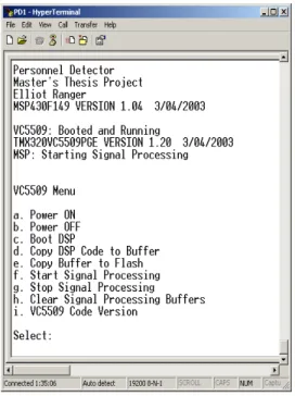
When the system is first powered the user is presented with the main menu shown
in Figure 3-3. The main menu has three standard sections. The header information
for the project is shown on the top of every screen. A message area is used to display
feedback to the user. The actual menu screen is in the center and allows the user
to select various submenus, such as, the VC5509 menu, Geophone menu, and ADC
menu. By pressing the letter associated with the menu the appropriate submenu is
brought up. These menus serve a dual purpose in the system. When the system
was designed this is how the system was tested. As various subsystems were brought
online they were tested by generating commands from the microcontroller to verify
that they were functioning correctly. Now, the menus serve to test the subsystems
again if something is not operating correctly and allow the user to make changes to
the system settings.
The VC5509 menu, Figure 3-4, regulates when the DSP is booted, how code gets
loaded into the DSP, and when signal processing is started. Also, this controls how
the DSP code gets saved into the flash of the microcontroller. First, the code is loaded
into a buffer location in the DSP memory and then it is transferred over to the flash of
the microcontroller. Starting the signal processing operation turns on the geophone
channel and starts the ADC on the microcontroller.
The Geophone menu, Figure 3-5, controls the geophone channels. The gain
set-tings can be modified for any of the channels, and power to the analog subsystem can
be turned on or off.
The ADC menu, Figure 3-6, allows the user to poll various channels on the ADC
to find out their instantaneous values. Both the geophone and test input channels
can be polled, and there is an internal temperature sensor in the microcontroller that
can be checked.
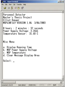
The Misc menu, Figure 3-7, has a few miscellaneous features that were
pro-grammed in the system, but not really necessary for normal operation. The
tem-perature can be checked and power supply voltage. The message area can be cleared,
and the running time of the processor since it was powered on can be displayed.
Port Description
The MSP has up to 48 digital I/O lines to control various subsystems and interface
with other components. Many of the ports on the MSP can be configured to perform
special functions as well. For instance, the ports that are used to receive the ADC
signals can either be selected as I/O ports or the inputs to the ADC. Obviously, when
the ports are selected to perform special functions it reduces the number of I/O ports
Figure 3-3: Main Menu
Figure 3-4: VC5509 Menu
Figure 3-7: Miscellaneous Menu
available. All of the I/O ports can be configured to read or write to the port. The
I/O ports are used to control the power for the DSP chip, seismic analog filtering and
amplification, the RF power, and RS232 chip. Furthermore, they are used to transfer
data back and forth between the DSP using the Host Port Interface (HPI).
The ports on the MSP are configured by writing to specific registers. Each port
has its own register to control: whether it is a port or special function, and the
direction of the port (read or write). There is a register to read the data from the
port or write data to the port. In addition to all the above configurations, Port 1 and
2 on the MSP are also able to receive interrupts as well. The ports are all set to their
initial values in the function initialize_ports() within the initialize_system()
routine. Table 3.2 shows the initial values of all the registers associated with each
of the ports. The PxSEL register determines if it is a special function (high) or the
standard port (low). PxDIR sets the direction of the port as either an output (high)
or input (low). PxIE enables the interrupts for the port. Interrupts can only be
enabled on port 1 and port 2. PxIES determines which edge the interrupt should
trigger on, the rising edge (low) or falling edge (high).
7 6 5 4 3 2 1 0 PORT 1 P1SEL P1DIR P1IE P1IES HRDY 0 0 0 0 HDS1 0 1 0 0 HR/W 0 1 0 0 HCNTL1 0 1 0 0 HCNTL0 0 1 0 0 HBE1 0 1 0 0 HINT 0 0 0 0 HBE0 0 1 0 0 PORT 2 P2SEL P2DIR P2IE P2IES HP7 0 0 0 0 HP6 0 0 0 0 HP5 0 0 0 0 HP4 0 0 0 0 HP3 0 0 0 0 HP2 0 0 0 0 HP0 0 0 0 0 HP1 0 0 0 0 PORT 3 P3SEL P3DIR RF_RXD 1 0 RF_TXD 1 0 UI_RXD 1 0 UI_TXD 1 0 RF_CTS 0 0 RF_ENA 0 1 VC55_ENA 0 1 GEO_ENA 0 1 PORT 4 P4SEL P4DIR HP15 0 0 HP14 0 0 HP13 0 0 HP12 0 0 HP11 0 0 HP10 0 0 HP8 0 0 HP9 0 0 PORT 5 P5SEL P5DIR RF_PWRDN 0 1 ACLK 1 1 RS232_ENA 0 1 MCLK 1 1 NOT USED 0 1 GEO_C_SEL 0 1 GEO_A_SEL 0 1 GEO_B_SEL 0 1 PORT 6 P6SEL P6DIR TEST_IN3 1 0 TEST_IN2 1 0 TEST_IN1 1 0 GEO_C_OUT 1 0 GEO_B_OUT 1 0 GEO_A_OUT 1 0 NOT USED 1 0 NOT USED 1 0