Analytical expression of top surface charge sensitivity
in fully depleted semiconductor on insulator MOS
transistor
Expression analytique de la sensibilité de la charge de surface avant pour
les transistors MOS semiconducteur sur isolant complètement déplétés
G. Ghibaudo1, G. Pananakakis1
1
IMEP-LAHC, Univ. Grenoble Alpes, Minatec/INPG, 3 Parvis Louis Neel, 38016 Grenoble, France
ABSTRACT. An analytical expression of free top surface charge sensitivity in FDSOI MOS structure has been established for weak inversion region and validated by TCAD numerical simulation. The influence of various FDSOI stack parameters has been analyzed. The impact of the interface trap density has been particularly emphasized, leading to a strong undesired degradation of sensitivity. This indicates that top surface passivation is a key issue for efficient charge sensing. These expressions of top surface charge sensitivity and associated threshold voltage shift should be very useful for sensor design and electrical characterization purpose.
KEYWORDS.charge sensitivity, FDSOI, threshold voltage, analytical expression.
1. Introduction
Field effect transistor (FET) based sensors are very attractive for their advantages in terms of miniaturization, integration, label-free detection and high sensitivity [BER03, STE07]. In this context, Ion Sensitive Field Effect Transistors (ISFET) have found applications as pH sensors. To improve the sensitivity of single gate ISFET, dual or double gate MOS devices with top and bottom gate electrodes have been introduced [IBA05, PAR14]. More recently, industrial grade FDSOI technology was employed to fabricate high sensitivity pH sensors, exploiting the huge front to back gate coupling in such fully depleted thin-film FET structure [MON16, RAH17]. In these FET sensors, the sensitivity is maximized when the transistor is operated in weak inversion i.e. subthreshold region, where front to back gate electrostatic coupling is not screened out by the channel formation.
Therefore, in this work, we aim at developing an analytical expression for the top surface charge sensitivity of FDSOI MOS transistors operated in weak inversion. This analytical expression could find several applications in FET sensor architecture design and electrical characterization.
2. Analytical modeling of surface charge sensitivity in FDSOI structure
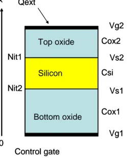
In a recent paper [GHI18], we have proposed analytical expressions for the subthreshold swing in FDSOI structure. To this aim, we have considered a 1D FDSOI structure (see Fig. 1) consisting of a fully depleted silicon film of thickness tsi (associated capacitance Csi) sandwiched by a top gate oxide of equivalent thickness tox2 (associated capacitance Cox2) and a bottom oxide of equivalent thickness tox1 (associated capacitance Cox1). The bottom (resp. top) silicon channel interface features an interface trap density Nit1 (resp. Nit2) with associated capacitance Cit1=q.Nit1 (resp. Cit2=q.Nit2). Gate voltage Vg1 (resp. Vg2) is directly applied to the bottom gate oxide (resp. top gate oxide). For free top surface, Vg2 is no longer applied on the top gate but is related to the top surface electric field controlled by the external charge Qext (see Eq. (1c) below). For simplicity, we assume undoped silicon film, which will have no impact on the subsequent charge sensitivity derivation.
Vg1 Vs1 Vs2 Vg2 x Bottom oxide Top oxide Silicon 0 Nit1 Nit2 Cox2 Csi Cox1 Qext Control gate Vg1 Vs1 Vs2 Vg2 x Bottom oxide Top oxide Silicon 0 Nit1 Nit2 Cox2 Csi Cox1 Qext Control gate
Figure 1. Schematic of 1D FDSOI structure under consideration for analytical calculation of top surface charge sensitivity.
Now, considering as in previous works [BAL90, WOU90, MAZ91, GHI18], that the free carrier charge in the channel can be neglected, which is of course verified in subthreshold region, and by turn, that the potential across the structure varies linearly with space, it is easy to show from Gauss’s law applied at top and bottom interfaces, that the front and back surface potentials are related by:
1 1 1 2 1 1 1 1 . . g ox si ox s ox si si ox si it s V C C C V C C C C C Q V (1a) 2 2 2 1 2 2 2 2 . . g ox si ox s ox si si ox si it s V C C C V C C C C C Q V (1b) 2 2 2 s ox ext g V C Q V (1c)
where Qit1=-q.Nit1.Vs1 and Qit2=-q.Nit2.Vs2 are the interface trap charges, q being the absolute electron charge.
After solving the system of Eqs (1) for the unknown Vs1 and Vs2 one obtains:
2 1 2 1 2 1 1 1 2 1 1 1 1 . . . . . . . . . . it it it ox it si it si ox si ext si g it ox g ox si s C C C C C C C C C C Q C V C C V C C V (2a) 2 1 2 1 2 1 1 1 1 1 1 2 . . . . . . . . . . it it it ox it si it si ox si ext it ext ox ext si g ox si s C C C C C C C C C C Q C Q C Q C V C C V . (2b)
Note that, in Eq. (2), we have overlooked the flat band voltage Vfb1. Otherwise, we should replace Vg1 by (Vg1-Vfb1) to account for it in Eq. (2).
Following [BAL90, GHI18], the free carrier inversion charge Qi can then be obtained by integration over silicon channel as:
. ( ). . . exp( 1) exp( 2) 2 1 0 kT qV kT qV V V t kT n q dx x n q Q s s s s si i tsi i (3)The top surface charge sensitivity, Sens=log(Qi)/Qext, can be computed with no approximation using Eqs (2) and (3), providing an exact calculation for the sensitivity. But, this set of equations does not constitute a close form analytical expression for the sensitivity. Therefore, we go one step further by rewriting Eq. (3) in the form:
12 12 1 exp 1 ln ) . . . ln( ) ln( s s s si i i V kT V q kT qV t kT n q Q (4)
where Vs12=Vs1-Vs2. Moreover, noting that Vs1 and Vs2 are very close in weak inversion, we make a first order expansion of Eq. (4) in Vs12, providing,
kT qV kT qV t kT n q kT V q kT qV t kT n q Qi i si s s i si s s 2 2 ) . . . ln( 2 ) . . . ln( ) ln( 1 12 1 2 . (5)
Then, we can evaluate the sensitivity from,
) ( . 2 ) ln( 1 2 ext s ext s ext i Q V Q V kT q Q Q Sens , (6)
which becomes using Eq. (2),
2 1 2 1 2 1 1 1 1 . . . . . . 2 . 2 si ox si it si it ox it it it it ox si C C C C C C C C C C C C C kT q Sens . (7)
As will be shown below from numerical simulation, Eq. (7) does provide an improved analytical expression for the top surface charge sensitivity in bottom gate operated FDSOI structures.
Finally, it is worth evaluating the threshold voltage shift Vth induced by the top surface external charge. To this end, we use the subthreshold swing (SW) expression found for FDSOI structure in [GHI18] and recalled in Eq. (8),
2 1 2 1 2 1 1 1 1 2 . . . 2 1 ) ln( ox si it it it it ox si ox it i g C C C C C C C C C C q kT Q V SW (8)In order to derive the threshold voltage shift as Vth= Sens.SW.Qext, which leads to the expression after combining Eqs (7) and (8):
ext C C C it ox si th Q C C C V it si ox . 2 ) 2 .( 1 1 2 . (9)
In absence of interface traps i.e. Cit1=Cit2=0, this expression reduces to,
ext si ox ox th Q C C C V . 2 1 1 . (10)
Note that Vth is not simply equal to Qext/Cox as it is often mentioned in the literature.
Moreover, looking at Eqs (7) and (10), it should be noted that the top surface charge sensitivity Sens and the associated threshold voltage shift Vth are independent of the top oxide thickness tox2. Actually, this is due to the fact that, in the case of a free surface configuration, the top surface is field (or charge) controlled and no longer voltage controlled, fully justifying this feature.
3. Results and discussion
In order to check the validity of the new analytical expression of Eq. (7) for the sensitivity Sens, we have analyzed the influence of the FDSOI stack parameters and trap density. A nominal FDSOI structure with tsi=10nm, tox1=10nm and tox2=2nm was considered unless specified. The analytical results were compared to exact simulations obtained by TCAD numerical resolution of the Poisson equation under classical statistics.
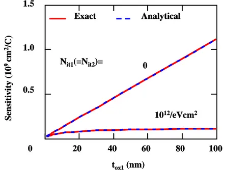
3.1. Influence of back gate oxide thickness
Typical variations of sensitivity Sens with back gate oxide thickness tox1 are illustrated in Fig. 2 as obtained from exact calculations (red solid lines) and the analytical expression of Eq. (7) for two interface trap densities with Nit1=Nit2 in the case of bottom gate operated FDSOI structure (tsi=10nm, Vg1=0.01V). Note the very good agreement obtained with the analytical formula of Eq. (7), especially for large interface trap density. It is worth noting that, for zero interface trap density, the sensitivity varies linearly with tox1, whereas it saturates rapidly with tox1 for large interface trap density.
1.5 1.0 0.5 0 20 40 60 80 100 tox1(nm) Sensi tivi ty (10 9 cm 2 /C) Exact Analytical Nit1(=Nit2)= 1012/eVcm2 0 1.5 1.0 0.5 0 20 40 60 80 100 tox1(nm) Sensi tivi ty (10 9 cm 2 /C) Exact
Exact AnalyticalAnalytical
Nit1(=Nit2)=
1012/eVcm2
0
Figure 2. Variation of sensitivity with bottom oxide thickness tox1. from exact calculations (red solid lines) and analytical expression of Eq. (7) (blue dashed lines) for two interface trap densities with Nit1=Nit2 in a bottom
gate operated FDSOI structure (tsi=10nm, tox2=2nm, Vg1=0.01V).
3.2. Influence of silicon film thickness
Typical variations of sensitivity Sens with silicon film thickness tsi are given in Fig. 3 as obtained from exact calculations (red solid lines) and analytical expression of Eq. 7 (blue dashed lines) for two interface trap densities with Nit1=Nit2 (tox1=10nm, tox2=2nm, Vg1=0.01V) in the case of bottom gate operated FDSOI structure. Note also the very good agreement achieved by the analytical equation (7), which well captures the increase of Sens with tsi. Similarly, the sensitivity varies almost linearly with tsi for zero interface trap density, whereas it tends to saturate for large interface trap density.
0 2.0 1.5 1.0 10 20 30 40 tsi(nm) Sensi tivi ty (10 8 cm 2 /C) 0.5 Nit1(=Nit2)= Exact Analytical 1012/eVcm2 0 0 2.0 1.5 1.0 10 20 30 40 tsi(nm) Sensi tivi ty (10 8 cm 2 /C) 0.5 Nit1(=Nit2)= Exact
Exact AnalyticalAnalytical
1012/eVcm2
0
Figure 3. Typical variations of sensitivity with silicon film thickness tsi from exact calculations (red solid lines) and analytical expression of Eq. (7) (blue dashed lines) for two interface trap densities with Nit1=Nit2 in a bottom
gate operated FDSOI structure (tox1=10nm, tox2=2nm, Vg1=0.01V).
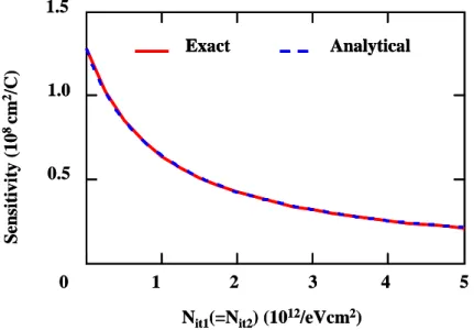
3.3. Influence of interface trap density
Typical variations of sensitivity Sens with interface trap density (Nit1=Nit2) are illustrated in Fig. 4 as obtained from exact calculations (red solid lines) and the analytical expression of Eq. (7) (blue dashed lines) in the case of bottom gate operated FDSOI structure (tsi=10nm, tox1=10nm, tox2=2nm, Vg1=0.01V). Here also, one should notice the very good description of the sensitivity as a function of the interface trap density provided by Eq. (7) and its strong degradation with increasing the interface trap density.
Finally, typical variations of threshold voltage shift Vth for Qext=1011q/cm2 with silicon film thickness tsi are illustrated in Fig. 5 as obtained from Eq. (9) for two interface trap densities Nit1=Nit2 in a bottom gate operated FDSOI structure (tox1=10nm, tox2=2nm). Note the noticeable reduction of the threshold voltage shift at large silicon film thickness for high trap density due to the increasing electrostatic screening of the top interface trap capacitance Cit2 in Eq. (9).
Nit1(=Nit2) (1012/eVcm2)
1.5 1.0 0.5 0 1 2 3 4 5 Se ns itiv ity (1 0 8 cm 2/C) Exact Analytical
Nit1(=Nit2) (1012/eVcm2)
1.5 1.0 0.5 0 1 2 3 4 5 Se ns itiv ity (1 0 8 cm 2/C) Exact
Exact AnalyticalAnalytical
Figure 4. Typical variation of sensitivity Sens with interface trap density (Nit1=Nit2) from exact calculations (red solid lines) and analytical expression of Eq. (7) (blue dashed lines) in a bottom gate operated FDSOI structure
0.05 0.1 0.15 0.2 V th (V ) @ Q ex t =1 0 11 q /cm 2 0 50 100 tsi(nm) Nit1(=Nit2)= 1012/eVcm2 0 0.05 0.1 0.15 0.2 V th (V ) @ Q ex t =1 0 11 q /cm 2 0 50 100 tsi(nm) Nit1(=Nit2)= 1012/eVcm2 0
Figure 5. Typical variations of threshold voltage shift Vth for Qext=1011q/cm2 with silicon film thickness tsi as obtained from Eq. (9) for two interface trap densities Nit1=Nit2 in a bottom gate operated FDSOI structure
(tox1=10nm, tox2=2nm).
6. Conclusions
An analytical expression of the free top surface charge sensitivity in FDSOI MOS structure has been established for weak inversion region and validated by TCAD numerical simulation. The influence of various FDSOI stack parameters has been analyzed. The impact of the interface trap density has been particularly emphasized, leading to a strong undesired degradation of sensitivity. This indicates that top surface passivation is a key issue for efficient charge sensing. These expressions of top surface charge sensitivity and associated threshold voltage shift should be very useful for sensor design and electrical characterization purpose.
Acknowledgements
This work has been partially supported by the H2020 European project Nanonets2sense under GAn°688329.
References
[BER 03] Bergveld P., Thirty years of ISFETOLOGY: what happened in the past 30 years and what may happen in the next 30 years, Sens Actuators B: Chem, 88, 1 (2003)
[STE 07] Stern E, et al., Label-free immunodetection with CMOS-compatible semiconducting Nanowires, Nature, 445, 519 (2007).
[IBA 05] Iba S, et al. Control of threshold voltage of organic field-effect transistors with double-gate structures, Appl. Phys. Lett., 87, 023509 (2005).
[PAR 14] Park J-K, et al, SOI dual-gate ISFET with variable oxide capacitance and channel thickness, Solid-State Electron, 97, 2 (2014).
[MON 16] Monfray S, Skotnicki T., UTBB FDSOI: evolution and opportunities, Solid-State Electron 125, 63 (2016). [RAH 17] L. Rahhal, et al, High sensitivity pH sensing on the BEOL of industrial FDSOI transistors, Solid-State
Electron, 134, 22 (2017).
[GHI 18] G. Ghibaudo and G. Pananakakis, Analytical expressions for subthreshold swing in FDSOI MOS structures, Solid State Electronics, 149, 57 (2018).
[WOU 90] D. J. Wouters, J. P. Colinge and H. Maes, Subthreshold Slope in Thin-Film SO1 MOSFET’s, IEEE Transactions on Electron Devices, 37, 2022, 1990.
[BAL 90] F. Balestra, et al, Analytical Models of Subthreshold Swing and Threshold Voltage for Thin- and Ultra-Thin-Film SOI MOSFET’s, IEEE Transactions on Electron Devices, vol. 37, 2303, 1990.
[MAZ 91] B. Mazhari, et al, Properties of Ultra-Thin Wafer-Bonded Silicon-on-Insulator MOSFET’s, IEEE Transactions on Electron Devices, 38, 1289, 1991.