HAL Id: hal-01169490
https://hal.archives-ouvertes.fr/hal-01169490
Submitted on 29 Jun 2015HAL is a multi-disciplinary open access archive for the deposit and dissemination of sci-entific research documents, whether they are pub-lished or not. The documents may come from teaching and research institutions in France or abroad, or from public or private research centers.
L’archive ouverte pluridisciplinaire HAL, est destinée au dépôt et à la diffusion de documents scientifiques de niveau recherche, publiés ou non, émanant des établissements d’enseignement et de recherche français ou étrangers, des laboratoires publics ou privés.
Dielectric properties of colossal permittivity materials:
An update
Chafé Cheballah, Zarel Valdez Nava, Lionel Laudebat, Thierry Lebey, Pierre
Bidan, Sombel Diaham, Sophie Guillemet-Fritsch
To cite this version:
Chafé Cheballah, Zarel Valdez Nava, Lionel Laudebat, Thierry Lebey, Pierre Bidan, et al.. Dielectric properties of colossal permittivity materials: An update. Journal of Energy and Power Engineering, David publishing compagny, 2013, vol. 7 (n° 4), pp. 726-732. �10.1109/CEIDP.2011.6232754�. �hal-01169490�
To cite this version : Cheballah, Chafe and Valdez-Nava, Zarel and
Laudebat, Lionel and Lebey, Thierry and Bidan, Pierre and Diaham,
Sombel and Guillemet-Fritsch, Sophie Dielectric properties of colossal
permittivity materials: An update. (2013) Journal of Energy and Power
Engineering, vol. 7 (n° 4). pp. 726-732. ISSN 1934-8975
O
pen
A
rchive
T
OULOUSE
A
rchive
O
uverte (
OATAO
)
OATAO is an open access repository that collects the work of Toulouse researchers and
makes it freely available over the web where possible.
This is an author-deposited version published in :
http://oatao.univ-toulouse.fr/
Eprints ID : 14110
Any correspondance concerning this service should be sent to the repository
administrator:
[email protected]
Dielectric Properties of Colossal Permittivity Materials:
An Update
Chafe Cheballah1, 2, Zarel Valdez-Nava1, 2, Lionel Laudebat3, Thierry Lebey1, 2, Pierre Bidan1, 2, Sombel Diaham1, 2 and Sophie Guillemet-Fritsch4
1. LAPLACE (Laboratoire Plasma et Conversion d'Energie), Université de Toulouse, Toulouse 9 F-31062, France 2. CNRS (Centre National de la Recherche Scientifique), LAPLACE, Toulouse F-31062, France
3. Centre Universitaire Jean-François Champollion, Albi 81012, France
4. Institut Carnot CIRIMAT (Centre Inter-universitaire de Recherche et d’Ingénierie des Matériaux), Université Paul Sabatier, Toulouse 9 31062, France
Abstract: During the last 10 years, a lot of interests have been devoted to the so-called CDC (colossal dielectric constant) materials.
The first materials exhibiting this behavior were the perovskite-based ceramics on the CCTO (CaCu3Ti4O12) composition. Relative
dielectric permittivity can attain values up to (or even larger than) 105. Nevertheless, their dielectric losses are too high, the lower values ranging 10%, in a narrow frequency range, thus limiting their applications. The underlying physical mechanisms at the origin of the CDC are still under study. The analysis of broadband impedance spectroscopy measurements leads most of the authors to propose an interfacial polarization mechanism (at the electrodes or at internal barriers), there is a limited number of complementary electrical characterization techniques, which, up to now, comfort the proposed interfacial polarization mechanisms. In the present work, I-V and time-domain polarization are used to characterize these materials. One of the main results is the observation of a non-symmetrical response of these materials related to the direction of the polarization. These results are observed for both macroscopic level on bulk polycrystalline material and within individual grains of the same samples. These results do not fit current accepted models for polarization for CDC materials.
Key words: Colossal permittivity, CaCu3Ti4O12, CCTO dielectric properties.
1. Introduction
Materials presenting the so-called colossal dielectric permittivity continue to attract a lot of attention since they were observed in CCTO (CaCu3Ti4O12) ceramics
[1]. These show a relative dielectric permittivity (!r) of up to 105 (at room temperature) that remains constant over a large temperature range with no apparent ferroelectric transition or phase transformations below 732 K [2]. These interesting properties that are stable with temperature make these materials suitable
Corresponding author: Zarel Valdez-Nava, Ph.D., CNRS
researcher, research fields: electroceramics, high-temperature ceramic dielectrics and colossal permittivity phenomena. E-mail: [email protected].
candidates for miniaturized capacitive elements in microelectronics. Despite the intensive works carried out to understand the physical origins of the high dielectric permittivity in polycrystalline ceramics [3], or in single crystals [4], or in thick and thin film layers [5], the exact role of both composition and microstructure on the electric properties of CCTO are still under study.
The earliest works intended to relate an intrinsic polarization to the crystalline structure. After inconclusive results [6], an extrinsic origin was proposed, assuming that interfaces were the key parameter on the polarization mechanism of CCTO.
First, these interfaces can be associated to the contact of the material to the electrodes [7], where the
differences in the metal work functions modify the dielectric response of the electrode-ceramic-electrode assembly. Supporting this hypothesis, Deng et al. [8] observed significant modification on the I-V
(current-voltage) characteristics related to the surface treatments on the samples. On the other hand, the characterization of polycrystalline CDC (colossal dielectric constant) materials by means of BIS (broadband impedance spectroscopy) identifies at least two distinct responses by equivalent circuit modeling [9]. It was suggested that one response corresponded to semiconducting grains, and the other to insulating grain boundaries. This analysis opened the way to another intrinsic barrier-induced polarization scheme, where the internal barriers formed by the grain boundaries acted as in IBLC (internal barrier layer capacitors). BIS remains the most used characterization technique for CDC materials [4, 9-13].
Only a limited number of studies using other characterization methods than BIS analysis in polycrystalline CDC materials have been reported. Local current-voltage (I-V) measurements using microelectrodes and local probe on polished CCTO confirmed the IBLC hypothesis, when Chung et al. [14] measured a barrier height at the grain boundary with a strong non-linear response. Scanning impedance microscopy and C-AFM (conductive atomic force microscopy), showed an insulating secondary-phase inclusion within a single CCTO grain [15]. Recently a controversy appeared [16], when Fu et al. [17] found that grain boundaries were also semiconducting and that grains were a mixture of semiconducting and insulating regions.
Further complementary characterization performed on colossal permittivity materials allowed to identify non-symmetrical response related to the applied voltage that is not taken into account by current accepted models [18]. In the present work, CCTO ceramics were analyzed by additional electrical characterization techniques, such as time-domain polarization at the bulk samples and I-V characterization, both for the bulk and
by locally probing the characteristics at the grain and grain boundary scale. Such studies were undertaken in order to add further elements to the discussion of the mechanisms involved in CDC materials polarization.
2. Experimental Procedure
The powders were prepared using a soft chemistry method described previously [19]. They were then pressed into pellets (5 mm diameter and 1.2 mm thickness) under 250 MPa and sintered in air at 1,050 °C for 24 h. The surfaces of the CCTO sample were polished (final thickness, 1.1 mm) and sputtered gold was applied as electrode.
Impedance spectroscopy measurements confirmed that the apparent permittivity of the samples presents the previously described characteristics of CDC materials [9, 20, 21].
In order to determine the influence of the electric field orientation on the electric response of the sample, each electrode was clearly identified “A” and “B”. A Keithley 2410 sourcemeter is used for I-V measurements, and in the measurement set-up, when the positive terminal of the sourcemeter is connected to the electrode on the sample surface “A”, the position is said to be “A (+)” and i “B (+)” in the opposite case (Fig. 1).
To perform local I-V characterizations at the grain and grain boundary scale, the CCTO pellet is sawed with a diamond wire cutting machine (ESCIL, W3241 model). The section was polished and thermally etched at 950 °C for 20 min to reveal the grain boundaries for optical observation. Scanning Electron Microscope (SEM-FEG, Jeol JSM 6700-F) coupled with an Energy Dispersive X-ray detector (EDX, Princeton Gamma Tech) and optical microscopy observations show large grain size distribution (up to 150 µm) with some pores at the surface (Fig. 2).
A thermo-regulated, microprobe station (Signatone S-1160 model) with tungsten probes (10µm in radius) is used to ensure local contact on the surface of the grains at 25 °C (Fig. 3). The two tungsten probes are connected to the Keithley 2410 sourcemeter.
Fig. 1 Definition of the two possible configurations for the sample.
Fig. 2 SEM micrograph of CCTO ceramics sintered at 1,050 °C for 24 h (bar 500 m).
Fig. 3 Microprobes configuration for I(V) measurements (a) within the grain and (b) across grain boundaries.
For time domain current measurements (I-t) a Keithley 6517A apparatus is used. Voltage steps are applied for polarization ranging from 0.1 V to 20 V. During the short-circuit of the sample, depolarization current is recorded.
3. Results and Discussion
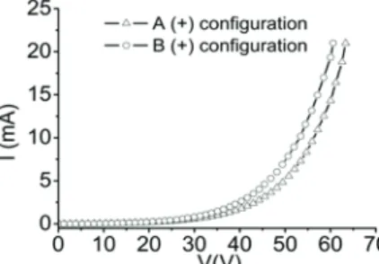
Fig. 4 shows the I-V measurements at room temperature. A non-linear characteristic is observed [14, 22]. However, when superposing the I-V responses of the “A (+)” and “B (+)” relative to the positive terminal of the sourcemeter, a non-symmetrical response of the sample is observed.
Fig. 4 Bulk I-V measurements for the CCTO ceramics in “A (+)” and “B (+)” configurations at room temperature.
These data are reproducible, either by changing the polarity of the applied voltage, when changing the wiring configuration, or when sample is turned upside down in the measured device cell. No memory effect can subsist since the sample is short-circuited for 5 min between every measurement (the current reaches a value of 0.2 pA).
The non linear I-V response has already been treated in other work and is assumed to be related to a Schottky contact allowing a potential barrier at the interface between grain and grain boundary [12, 23] or between the metal and the material [13, 24]. If the material is considered to be homogenous, only the interfaces between the CCTO ceramic and the metal electrode can explain the non-symmetrical phenomena. To check this assumption, the compositions determined from EDX analysis from each of the two sides (“A” and “B”) to the middle of the pellet were compared. Figs. 5a and 5b show that there is no significant difference in elemental composition of the pellet. So, if the chemical composition is homogeneous, the electrode contact can be one possible source for the difference of the electrical responses between the “A” and “B” configurations.
Deng et al. [5] have already observed this difference when applying platinum electrodes on thin-film CCTO with different PLD (pulsed laser deposition) conditions.
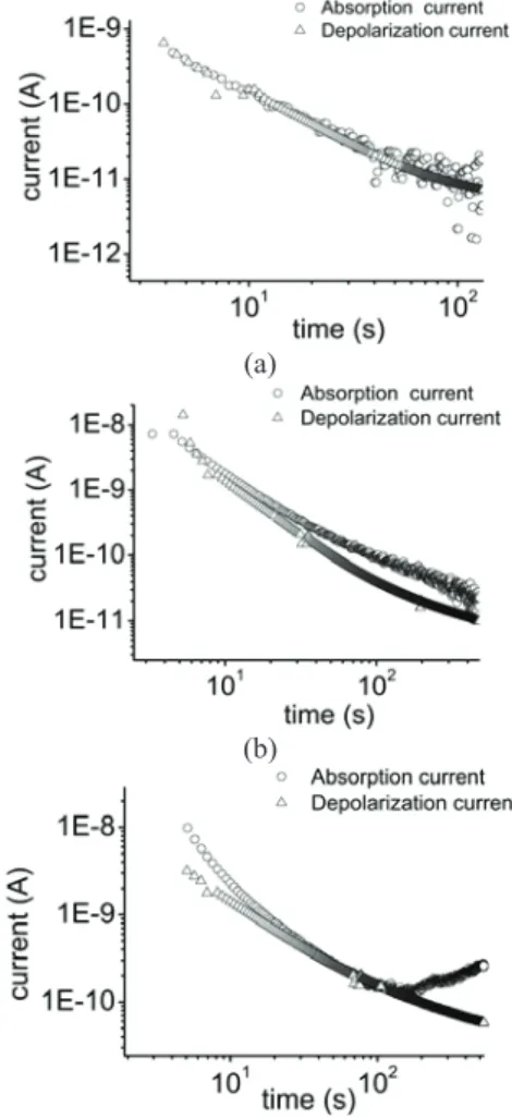
Fig. 6 shows I-t measurements for very low applied voltage (0.1 V). A quasi steady-state current is reached after 102 s. In conventional dielectric materials, when a step voltage is applied, the current evolution as function of time is composed of two phases:
(a) (b)
“A”
“A” “B”
Fig. 5 Elemental composition (EDX) from surfaces “A” and “B” at the center of the pellet.
Fig. 6 Polarization current for the CCTO ceramic with an applied voltage step of 0.1 V.
polarization and depolarization currents, as represented in Fig. 7. The polarization current is also composed of two parts, the absorption current mainly due to the polarization of dipoles in the dielectric, which dominates at short time, whereas the second part of the curve corresponds to the conduction current (Ic). The
absorption current of the CCTO sample (without Ic
contribution) and the absolute values of the depolarization current are super-imposable.
This behavior means that the stored charges in the material during polarization are restored during the depolarization.
In CCTO bulk sample, when absorption and depolarization currents are compared at low voltage, a dielectrical-like behavior as observed (Fig. 8a). This behavior exists up to 2 V (Figs. 8b and 8c).
For higher applied voltages (V > 2 V), the currents are no longer super-imposable (Fig. 9).
Fig. 7 Classical evolution of time-current response (Polarization and Depolarization) after an applied step voltage to a dielectric material.
(a)
(b)
(c)
Fig. 8 I-t polarization response of bulk CCTO at ambient T and (a) V = 0.1 V; (b) V = 1 V and (c) V = 2 V.
The very high values of the conduction current are shown in Fig. 10 (0.3 mA for 5 V), they are related to the strong non-linear I-V behavior of CCTO.
When probing the I-V response at a local level, care should be taken when interpreting surface measurement results, as the exact current path and the
Fig. 9 I-t response comparison between absorption and depolarization currents of bulk CCTO at room temperature and V = 5 V.
Fig. 10 I-t polarization response of bulk CCTO at ambient
T and V = 5 V.
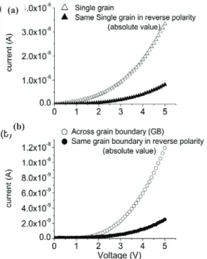
field distribution are unknown. The I-V responses of the grains and of the grain boundaries (Fig. 11) are both strongly non-linear. Furthermore, when reversing the voltage direction, thus, the current direction also, a non-symmetrical response is observed. Although different current values were observed between grain and across grain boundaries, due to the complexity of the measurements, only attention is given to their non-symmetrical behavior relative to the current direction.
When performing I-V probes measurement through gold electrodes contact, Chung et al. [14], where gold electrodes were previously applied to the sample. A strongly non-linear response of the I-V characteristic is observed whatever measurements are carried out through a grain boundary or in the grain. This behavior can be explained either by the intrinsic response of the CCTO or from a non-ohmic contact between the metallic tip and the specimen wherever it is contacted (inside a grain or between grain boundaries).
Fig. 11 I-V measurements characteristics (a) within grains and (b) across individual grain boundaries at 25 °C.
Surprisingly, it is also observed, as in the case in bulk materials, a non-symmetrical response on both grain and across grain boundaries that is dependent on the polarity applied with the sourcemeter (Fig. 11). Care was taken in order to avoid moving tips in between the measurements, and polarity is changed by inverting wires connected to the voltage source. This result means that the total current passing in one direction in the measurement setup (probe contact, then ceramic) is different from the one in the opposite direction.
One possible explanation of all these measurements could be that the contact between an electrode and the material whatever the scale level, can be considered as non-ohmic. The material could behave in that case as a MIS (metal-insulator-semiconductor) structure and the IBLC model is no more necessary to explain the different behaviors.
4. Conclusions
The use of characterization techniques that are complementary to impedance spectroscopy measurements, allowed to identify a non-symmetrical response relative to the applied voltage, in both bulk ceramic materials, and at the local level.
(a)
I-t measurements performed at different voltage levels, showed a high current related to the strong non-linear I-V response of CCTO. When the applied voltage step is higher than 2 V, absorption and desorption currents are no longer super-imposable in the CCTO ceramics. I-t measurement should complete, in future works, the panel of electrical characterization applied to this type of materials.
In regards to the I-V responses, for bulk ceramics, or for the grains and grain boundaries, the interfaces contact between the sample and the metal electrode seems to be the main key to explain the non-linear and non-symmetrical observed behaviors and a model like MIS structure can be a plausible explanation of these characteristics.
Further investigations concerning the interfaces CCTO/electrodes can lead to a better understanding of the non-linear and non-symmetrical I-V characteristics. The current models describing interfacial polarization, either electrode/surface polarization or IBLC do not take into account the non-symmetrical phenomena, meaning that a more comprehensible model is yet to be built.
References
[1] M.A. Subramanian, D. Li, N. Duan, B.A. Reisner, A.W. Sleight, High dielectric constant in ACu3Ti4O12 and
ACu3Ti3FeO12 phases, Journal of Solid State Chemistry
151 (2) (2000) 323-325.
[2] A. Onodera, M. Takesada, K. Kawatani, S. Hiramatsu, Dielectric properties and phase transition in CaCu3Ti4O12
at high temperatures, Japanese Journal of Applied Physics 47 (9) (2008) 7753-7756.
[3] S. Guillemet-Fritsch, T. Lebey, M. Boulos, B. Durand, Dielectric properties of CaCu3Ti4O12 based multiphased
ceramics, Journal of the European Ceramic Society 26 (7) (2006) 1245-1257.
[4] S. Krohns, P. Lunkenheimer, S. Ebbinghaus, A. Loidl, Broadband dielectric spectroscopy on single-crystalline and ceramic CaCu3Ti4O12, Applied Physics Letters 91 (2)
(2007) 022910-1-022910-3.
[5] G. Deng, Z. He, P. Muralt, Physical aspects of colossal dielectric constant material CaCu3Ti4O12 thin films,
Journal of Applied Physics 105 (8) (2009) 084106. [6] L. He, J. Neaton, M.H. Cohen, D. Vanderbilt, C.C. Homes,
First-principles study of the structure and lattice dielectric
response of CaCu3Ti4O12, Physical Review B 65 (21)
(2002) 214112-1-214112-11.
[7] P. Lunkenheimer, V. Bobnar, A. Pronin, A. Ritus, A. Volkov, A. Loidl, Origin of apparent colossal dielectric constants, Physical Review B 66 (5) (2002) 052105-1-052105-4.
[8] G. Deng, T. Yamada, P. Muralt, Evidence for the existence of a metal-insulator-semiconductor junction at the electrode interfaces of CaCu3Ti4O12thin film capacitors,
Applied Physics Letters 91 (20) (2007) 202903-1-202903-3.
[9] D.C. Sinclair, T.B. Adams, F.D. Morrison, A.R. West, CaCu3Ti4O12 one-step internal barrier layer capacitor,
Applied Physics Letters 80 (12) (2002) 2153-2155. [10] J. Sebald, S. Krohns, P. Lunkenheimer, S. Ebbinghaus, S.
Riegg, A. Reller, et al., Colossal dielectric constants: A common phenomenon in CaCu3Ti4O12 related materials,
Solid State Communications 150 (17) (2010) 857-860. [11] W.X. Yuan, Impedance and electric modulus approaches
to investigate four origins of giant dielectric constant in CaCu3Ti4O12 ceramics, Solid State Sciences 14 (3) (2012)
330-334.
[12] T.B. Adams, D.C. Sinclair, A.R. West, Giant barrier layer capacitance effects in CaCu3Ti4O12ceramics, Advanced
Materials 14 (18) (2002) 1321-1323.
[13] J. Yang, M. Shen, L. Fang, The electrode/sample contact effects on the dielectric properties of the CaCu3Ti4O12
ceramic, Materials Letters 59 (29-30) (2005) 3990-3993. [14] S.Y. Chung, I.D. Kim, S.J.L. Kang, Strong nonlinear current-voltage behaviour in perovskite-derivative calcium copper titanate, Nature Materials 3 (2004) 774-778. [15] P. Fiorenza, R. Lo Nigro, C. Bongiorno, V. Raineri, M.C.
Ferarrelli, D.C. Sinclair, et al., Localized electrical characterization of the giant permittivity effect in CaCu3Ti4O12ceramics, Applied Physics Letters 92 (18)
(2008) 182907-1-182907-3.
[16] S.Y. Chung, Comment on: Origin of giant dielectric response in nonferroelectric CaCu3Ti4O12:
Inhomogeneous conduction nature probed by atomic force microscopy, Chemistry of Materials 20 (19) (2008) 6284-6285.
[17] D. Fu, H. Taniguchi, T. Taniyama, M. Itoh, S.Y. Koshihara, Origin of giant dielectric response in nonferroelectric CaCu3Ti4O12: Inhomogeneous
conduction nature probed by atomic force microscopy, Chemistry of Materials 20 (5) (2008) 1694-1698. [18] Z. Valdez-Nava, S. Dinculescu, T. Lebey,
Non-symmetrical electric response in CaCu3Ti4O12and
La0.05Ba0.95TiO3-SPS materials, Journal of Physics D:
Applied Physics 43 (38) (2010) 385401-1-385401-6. [19] L. Marchin, S. Guillemet-Fritsch, B. Durand, A.
growth-controlled giant permittivity in soft chemistry CaCu3Ti4O12ceramics, Journal of the American Ceramic
Society 91 (2) (2008) 485-489.
[20] S. Krohns, P. Lunkenheimer, C. Kant, A.V. Pronin, H.B. Brom, A.A. Nugroho, et al., Colossal dielectric constant up to gigahertz at room temperature, Applied Physics Letters 94 (2009) 122903-1-122903-3.
[21] Z. Valdez-Nava, S. Guillemet-Fritsch, C. Tenailleau, T. Lebey, B. Durand, J.Y. Chane-Ching, Colossal dielectric permittivity of BaTiO3-based nanocrystalline ceramics
sintered by spark plasma sintering, Journal of Electroceramics 22 (1-3) (2009) 238-244.
[22] W. Li, R.W. Schwartz, Derivation and application of an empirical formula to describe interfacial relaxation effects in inhomogeneous materials, Journal of the American Ceramic Society 90 (11) (2007) 3536-3540.
[23] T.B. Adams, D.C. Sinclair, A.R. West, Characterization of grain boundary impedances in fine- and coarse-grained CaCu3Ti4O12 ceramics, Physical Review. B 73 (9) (2006)
094124-1-094124-9.
[24] G. Deng, P. Muralt, On origin and intrinsic electrical properties of the colossal dielectric constant state in CaCu3Ti4O12, IOP Conf. Series: Materials Science and