HAL Id: hal-01712749
https://hal.archives-ouvertes.fr/hal-01712749
Submitted on 19 Jun 2018
HAL is a multi-disciplinary open access
archive for the deposit and dissemination of
sci-entific research documents, whether they are
pub-lished or not. The documents may come from
L’archive ouverte pluridisciplinaire HAL, est
destinée au dépôt et à la diffusion de documents
scientifiques de niveau recherche, publiés ou non,
émanant des établissements d’enseignement et de
Quantum half-adder Boolean logic gate with a
nano-graphene molecule and graphene nano-electrodes
Saurabh Srivastava, Hiori Kino, Christian Joachim
To cite this version:
Saurabh Srivastava, Hiori Kino, Christian Joachim. Quantum half-adder Boolean logic gate with a
nano-graphene molecule and graphene nano-electrodes. Chemical Physics Letters, Elsevier, 2017, 667,
pp.301-306. �10.1016/j.cplett.2016.11.009�. �hal-01712749�
Quantum Half-Adder Boolean Logic Gate with a
Nano-Graphene molecule and Graphene
Nano-electrodes
Saurabh Srivastavaa,∗, Hiori Kinoa, Christian Joachimb,a,∗
aWPI-MANA, National Institute for Material Sciences, 1-1 Namiki, Tsukuba, Ibaraki,
Japan
bCEMES-CNRS, 29 Rue J. Marvig, BP 4347, 31055 Toulouse Cedex, France
Abstract
A molecule Boolean 1/2-adder is designed and the XOR and AND truth table
calculated at +0.1 V using 4 graphene electrodes. It functions with level
re-pulsion and destructive interferences effects using 4 molecule electronic states
in a quantum Hamiltonian computing approach (QHC) with the abrupt change of the molecular orbital weight of those 4 calculating states as a function of
the logical input configuration. The logical inputs enter rotating the two nitro
groups of the central board. With QHC, a complex Boolean digital function
can be implemented employing the same graphene material for interconnects
and the molecule calculating parts.
Keywords: Graphene, Logic Gates, Quantum Transport, Quantum
Computing, Molecular electronics, Half-Adder
1. Introduction
The continuing miniaturization of electronic circuits triggers the ultimate
search for single molecule based electronics where a molecule embedded between
many electrodes will perform a digital Boolean function by itself[1, 2]. One
pos-sibility is to interconnect molecular switches[3, 4], rectifiers[5, 6] or amplifiers[7]
5
∗Corresponding author
Email addresses: [email protected] (Saurabh Srivastava), [email protected] (Christian Joachim)
together using metallic nanowires[8] to construct the circuit. This approach is
now progressively abandoned due to the absence of power gain per molecular
device[9]. Semi-classically designed intramolecular circuits[10] have also been explored[11] facing now the problem of the exponential decay of the output
current with an increase of the spatial extension of the molecular circuit[12].
10
To solve those gain and exponential decay problems still with the objective
to embark a calculating unit on a single molecule, a new quantum
comput-ing approach was proposed[13].When prepared in a non-stationary state, the
quantum Hamiltonian computing (QHC) logic gate beneficiates from the spon-taneous Heisenberg-Rabi quantum oscillations of the quantum system to run
15
a quantum computation with classical inputs[14]. By measuring the effecting
Heisenberg-Rabi oscillations frequency using metallic nano-electrodes[15],
dif-ferent Boolean logic operations can be performed in parallel and within the same quantum system[16]. The functioning of a Boolean QHC gate is based
on the quantum level repulsion effect together with the control of constructive
20
and destructive quantum interferencesaffectingtunneling transport. Quantum
design rules for QHC single molecule logic gates have been reported by Renaud
et al.[13]. Following this approach, Soe et al.[17] have demonstrated
experimen-tally a NOR logic gate function using a tri-naphthalene molecule whose frontiers
molecular orbitals were manipulated by single Au atom contact to each of the
25
naphthyl branch. Formally, A different QHC design was used to structure a
single molecule NOR-AND[18]gate. For the previous hybrid 1/2-adder Boolean
logic functions[19, 20], rotation of two lateral nitro chemical groups were also providing the classical digital inputs to the QHC gate here with a direct con-version of each rotation angle in quantum information. This concon-version can be
30
exactly measured by decomposing each molecular state on its Slater atomic
ba-sis set. It shows how a given NO2rotation angle is encoded on the normalized
atomic orbital coefficients of certain molecular states.
For these QHC molecule Boolean logic gates, metallic nano-electrodes were
used to measure the logical outcome of the gates. Such metal-organic hybrids
35
differ-ence in electronic structure between the central calculating molecule unit and
its metallic measuring nano-electrodes. To design more complex QHC molecule
logic gates (for exploring how the QHC approach can do better in term of deco-herence as compared to the quantum qubit approach[21]) and for beneficiating
40
in application of tunneling current intensities larger than a few nano-ampere,
the calculating molecule and the measuring electrodes must be made of the
same material. The graphene planar 2D material with its tunable electronic,
mechanical and electronic properties[22, 23, 24] is an excellent candidate for a
monolithic approach of QHC molecular logic gates.
45
In this letter, we demonstrate theoretically that a double nitro
function-alized nano-graphene molecule (NGM) connected using graphene electrodes is
performing a 1/2 adder Boolean operation in the QHC way using the rotation
of the nitro-groups as the classical digital inputs. The first section is describing the QHC NGM design. Section 2 is recalling the technique used in this
let-50
ter to calculate all the tunneling current intensity passing through the central
NGM. Section 3 is describing the functioning of our 1/2 adder QHC NGM. In
conclusion, we compare our design with a classical 1/2 adder electronic circuit.
2. The Boolean 1/2 adder QHC molecular design
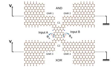
On Fig. 1, a central NGM is chemically bonded to 4 ultra-short 3 phenyls
55
in length and 2in width graphene nano-ribbon (GNR1 to GNR4). The core of
the NGM molecule was designed starting from a coronene molecule extended asymmetrically by phenyl rings to be able to distinguish an AND and an XOR functionality by its MO weight at the measuring point. Four different
conju-gated boards were tested not to extend too much this central NGM.Each GNR
60
is connected to independent semi-infinite graphene electrode whose electronic
band structure is well defined using periodic boundary conditions[30]. The
cen-tral NGM is 2D crystal oriented in the same direction as the graphene electrodes to beneficiate from a complete homo electronic structure between the NGM and
its measuring graphene electrodes. Nano-graphene molecules have already been
synthesized[25]. The Fig. 1 NGM circuit may be nanoscale fabricated for its
in-terconnection parts using a high precision He+scattering [26] and using scanning tunneling microscope (STM) single atom vertical manipulations for the atomic
scale part as already demonstrated at the surface of 2D MoS2 materials[27]. In
Fig. 1, the A and B nitro group inputs were chemically bonded to the NGM
70
for distributing the logical inputs between the XOR and AND part of the QHC
circuitwithout requiring ancillary internal or external molecular wires as
com-monly performed in standard electronic Boolean logic circuits. In electronics, the output of a given gate along the circuit is generally required to distribute its output signal at many locations of the circuit at the same time. Our present
75
molecule QHC design can be considered as a practical implementation of the formal QHC 1/2-adder[16] where it was shown how to position the logical inputs along the QHC quantum graph to avoid this cascading problem. Two fluorine
atoms were also added to the NGM to optimize, as presented in Fig. 4, the
distribution of the frontier molecular orbitals over the NGM depending on the
80
logical input configuration as discussed later. With respect to the graphene
electrode plane, a planar nitro is encoding for a “0” binary logical input and a
perpendicular one for a “1” logical input. This encoding was chosen because of
thenon-zero switching energy certainly required to input a logical “1” on the
NGM by STM rotating a single NO2 group, as it was already demonstrated for
85
a single ter-butyl group [28],the native nitro configuration being planar[29]. A
nitro group is a small but very efficient electron acceptor group, very active in
interacting with a conjugated molecule while co-planar with it[30, 31].
3. The Calculation Technique
Through the Fig. 1 QHC circuit and using Landauer formula[32, 33], the
90
current intensity I was calculated between any two graphene electrodes and
when applying a bias voltage V using :
I = e π¯h
Z Ef+eV
Ef
where Ef is the Fermi energy of a given graphene electrode and T (E) =
Trace(t(E)t†(E)), the electronic transparency between those two graphene
elec-trodes. t(E) is the top left block of the multi-channel elastic scattering matrix
95
describing the scattering process through the central NGM. The complete
multi-channel scattering matrix was calculated exactly using the elastic scattering
quantum chemistry (ESQC) method[16, 34, 35]. A full valence semi-empirical
Hamiltonian was used in ESQC to describe the central molecule along with
its 4 short GNR molecular wires and the graphene electrodes. This
Hamilto-100
nian was constructed with the full valence extended H¨uckel molecular orbitals
(EHMO) basis set using Hoffmann parameters[36, 37] for all the C, N, O, F, and
H atoms. A discussion about the Hoffmann parameters preferred over C´erda
parameters[38, 39] can be found in [30] for graphene. Using those EHMO
param-eters, the calculated graphene electrode band structure shows a relative energy
105
position of the Dirac cone crossing point at E = Ef = −10.53 eV.
4. The functioning of the nano-graphene QHC 1/2 adder
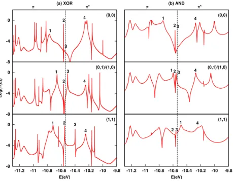
In Fig. 2, the calculated T(E) spectra for the XOR and AND outputs are
presented as a function of the A and B logical input configurations. The cross
“leakage” T(E) spectra between one XOR and one AND graphene electrodes,
110
respectively, through the NGM were also calculated and according to equation
1 lead to a less than 0.01 µA tunneling current intensity for a 0.1 V bias voltage
as compared with the direct XOR and AND outputs. This is the maximum
calculated leakage current from one XOR to one AND graphene electrodes and for only the (1,1) input configuration. A 0.01µA current intensity on the AND
115
for (1, 1) is not very noticeable as compared to the 2µA measured output cur-rent for this input configuration. All the others cross leakage curcur-rent are one order of magnitude lower than 0.01µA at 0.1 V for all the other logical input
configurations. The T (E) spectra are showing up some π and π∗resonances
to-gether with destructive interference patternsi.e. very pronounced s in the T(E)
120
eV for the AND (0, 1)/(1, 0) configurations. The functioning of the Fig. 1 QHC
1/2 adder is based on the quantum level repulsion effect and on an optimized
energy positioning of those tunneling destructive interferences relative to the graphene Fermi energy. As also demonstrated recently with a formal Boolean
125
Hamiltonian, having two outputs for the same QHC system and measured in
the same energy range requires that the weight of the molecular orbitals at
mea-surement points (here C1 and C2) be quite exclusive as a function of the input
configuration[16].
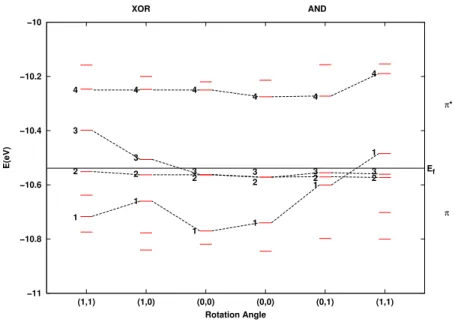
Let us first start with the level repulsion effect. Among all the π and π∗
130
molecular orbitals of the central NGM and in an energy range 2 eV around the
Fermi energy, only a few are effectively contributing to the 1/2 adder
function-ing because many have no molecular weight at the C1 and C2 chemical bondfunction-ing
sites of the graphene electrodes. We have identified on Fig. 2, the 4 main “cal-culating” molecular states of the central NGM i.e. the T(E) spectra resonances
135
contributing the most to the 1/2 adder functioning. They have been labeled 1
to 4 for mono-electronic quantum states |1i to |4i (For completion and in the
Suppl. Mat. 5, they are also labeled on the corresponding complete spectrum
of this central NGM alone). For clarity, Fig. 3 is only showing up the energy
position of those 4 states in a quantum level correlation diagram. There is a
140
clear level repulsion effect in action on state |1i shifted up in energy by about 0.3
eV and on state |3i by about 0.2 eV by going from a parallel to a perpendicular
nitro conformationsfor AND and XOR respectively.
Based on this level repulsion effect, the functioning of the Fig. 1 1/2 adder QHC gate is also relaying on the control by the nitro angles of the T (E)
con-145
structive and destructive interference patterns. Notice that, those patterns also
depend on the chemical structure of contact C1 and C2. For a (0, 0) logical
input i.e. for two planar nitro’s, there is a very pronounced T (E) destructive
interference between states |1i and |4i at E = −10.49 eV for the XOR T (E) and
at E = −10.51 eV for the AND T (E). Located near the Fermi energy and at
150
low positive bias voltage, this will leads to a very low output current according
the AND. Notice that, the two very sharp resonances located just below the
Fermi energy are coming from states |1i and |3i which are only weakly coupled
to the graphene electrodes for (0, 0). They will not contribute to the XOR and
155
AND logical outputs in this case.
The (0, 0) input destructive interference patterns are drasticallychanged by
rotation ofthe nitro group one after the other from a planar to a
perpendicu-lar conformation (See Suppl. Mat. 6 for the detail T(E) interference pattern
changes following the progressive rotation of the two nitro groups). For the (0, 1)
160
and (1, 0) input configurations, the (0, 0) XOR central destructive interference
observed previously at E = −10.49 eV is now shifted below the Fermi energy
and state |3i leads now to a very sharp constructive resonance positioned up the
Fermi energy at E = −10.50 eV. This results from the restoration of the
elec-tronic coupling between state |3i and the two GNR3 and GNR4 nano-contacts
165
after reaching a perpendicular conformation for only one nitro group having
the effect of reintroducing an electronic density expansion of |3i at contact C2
(see also below Fig. 4). The resonance from state |2i is still very sharp and
will not contribute to the tunneling current because it is deeply attenuated by
the central destructive interference located at E = −10.55 eV. Also for (0, 1)
170
and (1, 0), the AND central destructive interference is shifted up and above the
Fermi energy at E = −10.35 eV. Here, state |3i is still leading to a very sharp
resonance below the Fermi energy. State |3i will not contribute to the AND
tunneling current output.
For the (1, 1) input configuration, the XOR central destructive interference
175
is still located below the Fermi energy and state |2i resonance remains below the
Fermi energy. More important, the resonance coming from |3i is still very sharp
and now shifted up further away from the Fermi energy. This means that at
low bias voltage and according to equation 1, it will not contribute to the XOR
tunneling current. Also for (1, 1), the AND destructive interference between |1i
180
and |4i which was located for (0, 1) and (1, 0) at E = −13.35 eV is now no more
existing. The state |1i resonance has now reached E = −10.49 eV with a large
equation 1, this will lead to the AND output functioning.
According to the T(E) spectra in Fig. 2, both the XOR and AND output
185
status must be measured in an energy range about 0.1 eV up the Fermi energy. As a consequence, the chemical structure of the C1 and C2 contacts have been
designed differently to be able to distinguish between the XOR and AND
out-put because they are resonating almost at the same energy. The effect of this
different design between the C1 and C2 contacts can be observed around the
190
state |4i resonances by comparing the structure of the corresponding resonance
massif for the XOR and the AND. It was demonstrated in Hosoki et al. [27] that
when measuring at the same energy the 2 different logical outputs on the same
QHC system (here the XOR and the AND), one need a very abrupt change of
the weight of the corresponding orbitals as a function of the logical input to
195
be able to spatially distinguish 2 outputs at the same energy. As presented in Fig. 4, this is exactly what was achieved with the Fig. 1 design thanks also to
the substitution of2 hydrogen atoms by 2 fluorine atomson the central NGM.
By representing states |1i and |3i corresponding molecular orbital normalized
weight distribution on the NGM, it is clear that only the input configuration
200
(1, 1) is leading to a large orbital weight for |1i at C1 for the AND. Only input
configurations (0, 1) and (1, 0) are doing the same for |3i at C2. This exclusive
distribution of the molecular orbital spatial weight determines the good
func-tioning of our 1/2 adder QHC gate. It is exactly the chemical implantation of
the formal Boolean Hamiltonian studied in Dridi et. al [16].
205
5. Discussion
Using the Fig. 2 T(E) spectra in equation 1 to calculate the 0.1 V low
voltage tunneling current intensity passing through the central NGM at C1 and
C2, the 1/2 adder Boolean truth table is presented in Table 1. According to the
standard C. Shannon like design[40], a Boolean 1/2 adder is normally requiring
210
the interconnection of a minimum of 4 transistors and a dedicated distribution
circuit nodes. The presented 232 atoms nano-graphene calculating molecule
has no transistors nor apparent internal molecular wires like circuitry. Among
the 168 π and π∗ quantum states of the Fig. 1 central nano-graphene molecule,
215
mainly 4 states are “calculating” as presented in Fig. 3. The NGM quantum
states |1i and |3i are shifted up because of the rotation of 2 strong electron
acceptor groups. Those are classical mechanical inputs which cancertainly be
activated by scanning probe techniques but has not been experimented yet.
State |4i is very important to create the (0, 0) central destructive interference
220
and state |2i to moderate the (1, 1) XOR output current to ensure a low output
current for this input configuration. Nearby in energy to those 4 states, a
few more are moderating the level repulsion acting on |1i and |3i to limit, for
example, the shifting up of the resonances |1i and |3i while rotating the nitro
groups. All the other NGM quantum states can be considered as structural
225
states ensuring the chemical stability of the central nano-graphene molecule.
Importantly the XOR and AND output current intensities are quite large. First because the tunneling electrons have not to be transferred through the complete NGM molecular structure to deliver each output status. Second because the measuring pads are homo electronic with the central calculating nano-230
graphene, a way to optimize the contact conductance at C1 and C2.
Our nano-graphene QHC 1/2-adder demonstrates how a small molecular nanostructure can performed a rather complex logic function: a binary addition with a carry without using an extended molecular system but more impor-tant without requiring any power gain inside the calculating board. The
non-235
necessity of a power gain comes from the fact that the output status of the gate are measured without passing a current through to the entire molecule. Con-trary to previous proposed QHC 1/2- adder design [20], it results from a local measurement. This new QHC design opens the search for more complex and monolithic QHC intramolecular logic gates based on intramolecular quantum
240
Acknowledgement
SS thanks the MANA-NIMS Theory-Experiment Fusion Research Program
and the NIMS computation facilities. CJ thanks the WPI MANA program for
financial support and the constant encouragements of Pr. M. Aono during this
245
work.
References
[1] C. Joachim, J. K. Gimzewski, A. Aviram, Electronics using
hybrid-molecular and mono-hybrid-molecular devices, Nature 408 (2000) 541–548.
[2] W. X. Zhang, Voltage-driven spintronic logic gates in graphene
nanorib-250
bons, Scientific Reports 4 (2014) 6320–1–6320–4.
[3] C. P. Collier, E. W. Wong, M. Belohradsk, F. M. Raymo, J. F.
Stod-dart, P. J. Kuekes, R. S. Williams, J. R. Heath, Electronically configurable
molecular-based logic gates, Science 285 (1999) 391–394.
[4] C. P. Collier, G. Mattersteig, E. W. Wong, Y. Luo, K. Beverly, J. Sampaio,
255
F. M. Raymo, J. F. Stoddart, J. R. Heath, A [2]catenane-based solid state
electronically reconfigurable switch, Science 289 (2000) 1172–1175.
[5] R. M. Metzger, All about
(n-hexadecylquinolin-4-ium-1-yl)methylidenetricyanoquinodimethanide, a unimolecular rectifier of
electrical current, J. Mater. Chem. 10 (2000) 55–62.
260
[6] R. M. Metzger, Electrical rectification by a molecule:the advent of
uni-molecular electronic devices, Acc. Chem. Res. 32 (1999) 950–957.
[7] C. Joachim, J. Gimzewski, An electromechanical amplifier using a single
molecule, Chem. Phys. Lett. 265 (1997) 353–357.
[8] S. Ami, C. Joachim, Logic gates and memory cellsbased on single c60
elec-265
[9] R. Staddler, S. Ami, M. Forshow, C. Joachim, A memory/adder model
based on single c60 molecular transistors, Nanotechnology 12 (2001) 350–
357.
[10] J. Ellenbogen, J. Love, Architectures for molecular electronic computers.
270
i. logic structures and an adder designed from molecular electronic diodes,
Proc. IEEE 88 (2000) 386–426.
[11] N. Jlidat, M. Hliwa, C. Joachim, A semi-classical xor logic gate integrated
in a single molecule, Chem. Phys. Lett. 451 (2008) 270–275.
[12] L. Lafferentz, F. Ample, H. Yu, S. Hercht, C. Joachim, L. Grill,
Conduc-275
tance of a single conjugated polymer as a continuous function of its length,
Science 323 (2009) 1193.
[13] N. Renaud, M. Hliwa, C. Joachim, Quantum design rules for single molecule logic gates, Phys. Chem. Chem. Phys. 13 (2011) 14404–14416.
[14] N. Renaud, C. Joachim, Design and stability of nor and nand logic gates
280
constructed with three quantum state, Phys. Rev. A 78 (2008) 062316–1–
062316–10.
[15] O. Faizy, G. Dridi, C. Joachim, Parallel quantum circuit in a tunnel
junc-tion, Sci. Rep. 6 (2016) 30198–1–30198–10.
[16] G. Dridi, R. Julien, M. Hliwa, C. Joachim, The mathematics of a quantum
285
hamiltonian computing half adder boolean logic gate, Nanotechnology 26
(2015) 344003.
[17] W.-H. Soe, C. Manzano, N. Renaud, P. de Mendoza, A. D. Sarkar, F.
Am-ple, M. Hliwa, A. M. Echavarren, N. Chandrasekhar, C. Joachim,
Manipu-lating molecular quantum states with classical metal atom inputs:
Demon-290
stration of a single molecule nor logic gate, ACS Nano 5 (2011) 1436–1440.
[18] N. Renaud, M. Ito, W. Shangguan, M. Saeys, M. Hliwa, C. Joachim, A
norand quantum running gate molecule, Chem. Phys. Lett. 472 (2009) 74–
[19] I. Duchemin, C. Joachim, A quantum digital half adder inside a single
295
molecule, Chem. Phys. Lett. 406 (2005) 167–172.
[20] I. Duchemin, N. Renaud, C. Joachim, An intramolecular digital 1/2-adder with tunneling current drive and read-outs, Chem. Phys. Lett. 452 (2008)
269–274.
[21] M. Nielsen, I. L. Chuang, Quantum Computation and Quantum
Informa-300
tion, Cambridge University Press, London, 2000.
[22] A. K. Geim, K. S. Novoselov, The rise of graphene, Nat. Mater. 6 (2007)
183–191.
[23] K. S. Novoselov, A. K. Geim, S. V. Morozov, D. Jiang, Y. Zhang, S. V.
Dubonos, I. V. Grigorieva, A. A. Firsov, Electric field effect in atomically
305
thin carbon films, Science 306 (2004) 666–669.
[24] K. S. Novoselov, A. K. Geim, S. V. Morozov, D. Jiang, M. I. Katsnelson,
I. V. Grigorieva, S. V. Dubonos, A. A. Firsov, Two-dimensional gas of
massless dirac fermions in graphene, Nature 438 (2005) 197–200.
[25] R. Dorel, C. Manzano, M. Grisolia, W. Soe, C. Joachim, A. M. Echavaren,
310
Tetrabenzocircumpyrene: a nanographene fragment with an embedded
peripentacene core, Chem. Comm. 51 (2015) 6932–6935.
[26] S. Nakaharai, T. Iijima, S. Ogawa, S. Suzuki, S.-L. Li, K. Tsukagoshi,
S. Sato, N. Yokoyama, Conduction tuning of graphene based on defect-induced localization, ACS Nano 7 (2013) 5694–5700.
315
[27] S. Hosoki, S. Hosaka, T. Hasegawa, Surface modification of mos2using an
stm, Appl. Surf. Sci. 60 (1992) 643–647.
[28] C. Loppacher, M. Barmmerlin, M. Guggisberg, O. Pfeiffer, E. Meyer,
R. Luthi, R. Schlitler, J. K. Gimzewski, H. Tang, C. Joachim, Direct
deter-mination of the energy required to operate a single molecule switch, Phys.
320
[29] A. Domenicano, G. Schultz, I. Hargittai, M. Colapietro, G. Portalone,
P. George, C. W. Bock, Molecular structure of nitrobenzene in the
pla-nar and orthogonal conformations, Struct. Chem. 1 (1990) 107–122.
[30] S. Srivastava, H. Kino, C. Joachim, Contact conductance of a graphene
325
nanoribbons with its graphene nano-electrodes, Nanoscale 8 (2016) 9265–
9271.
[31] C. Patoux, C. Coudret, J. Launay, C. Joachim, A. Gourdon, Topological
effects on intramolecular electron transfer via quantum interference,
Inor-ganic Chemistry 36 (1997) 5037–5049.
330
[32] M. Buttiker, Y. Imry, R. Landauer, S. Pinhas, Generalized many-channel
conductance formula with application to small rings, Phys. Rev. B 31 (1985)
6207–6215.
[33] A. D. Stone, A. Szafer, What is measured when you measure a
resistance?-the landauer formula revisited, IBM J. Res. Dev. 32 (1988) 384–413.
335
[34] P. Doumergue, L. Pizzagalli, C. Joachim, A. Altibelli, A. Baratoff,
Con-ductance of a finite missing hydrogen atomic line on si(001)-(2x1)-h, Phys.
Rev. B 59 (1999) 15910–15916.
[35] K. S. Yong, D. M. Otalvaro, I. Duchemin, M. Saeys, C. Joachim,
Calcula-tion of the conductance of a finite atomic line of sulfur vacancies created on
340
a molybdenum disulfide surface, Phys. Rev. B 77 (2008) 205429–1–205429– 9.
[36] R. Hoffmann, An extended h¨uckel theory. i. hydrocarbons, J. Chem. Phys.
39 (1963) 1397–1412.
[37] M. Wolfsberg, L. J. Helmholz, The spectra and electronic structure of the
345
tetrahedral ions mno−4, cro−−4 , and clo−4, J. Chem. Phys. 20 (1952) 837–843.
[38] J. Cerd´a, F. Soria, Accurate and transferable extended h¨uckel-type
[39] D. Kienle, J. Cerd´a, A. W. Ghosh, Extended h¨uckel theory for band
struc-ture, chemistry, and transport. i. carbon nanotubes, J. of Appl. Phys. 100
350
(2006) 043714–1–043714–9.
[40] F. Carter, The molecular device computer: Point of departure for large
Input A Input B XOR AND C1 C2 GNR 1 GNR 2 GNR 4 GNR 3 o o B A
Figure 1: The atomic structure of the designed QHC 1/2 adder nano-graphene molecular logic gate with its 4 ultra-short GNR interconnecting molecular wires (GNR1 to GNR4) and its 4 graphene electrodes. The AND is measured at contact C1 and the XOR at contact C2.
Contacts C1 and C2 are made of 2 phenyl rings each for the tunneling current to be measured between GNR1 and GNR2 for C1 and between GNR3 and GNR4 for C2. The graphene electrodes are semi-infinite to work with the grapheneelectronicband structurereproduced here using lateral cyclic boundary conditions. The two fluorine atoms are shown in blue whereas the two rotating nitro groups are shown in red. The presented geometry is for the nitro-groups in a planar configuration encoding for a (0, 0) logical input.
-8 -4 0 (a) XOR π π* (0,0) 1 2 3 4 -8 -4 0 Log(T(E)) (0,1)/(1,0) 1 2 3 4 -8 -4 0 -11.2 -11 -10.8 -10.6 -10.4 -10.2 -10 -9.8 E(eV) (1,1) 1 2 3 4 (b) AND π π* (0,0) 1 2 3 4 (0,1)/(1,0) 1 2 3 4 -11.2 -11 -10.8 -10.6 -10.4 -10.2 -10 -9.8 E(eV) (1,1) 1 2 3 4
Figure 2: The ESQC calculated T (E) electronic transmission coefficients for (a) the XOR and (b) the AND logical outputs as a function of the logical input configurations. For the [-11.3 eV, -11.0 eV], [-10.0, -9.8 eV] XOR energy intervals and for the [-11.3 eV, -10.9 eV], [-10.1 eV, -9.8 eV] AND energy intervals, the T(E) remain unchanged while the resonances are moving in energy around the graphene Fermi energy. A zoom-in of this last part is also presented in Suppl. Mat. Fig. 6. For (0, 0), the destructive interference between |1i and |4i is ensuring a zero logical output current intensity. The level repulsion effect controlled by the nitro rotations is pushing up |1i and |3i for respectively the AND and the XOR. This is changing the T (E) interference patterns leading to the adder functioning. States |2i for the XOR and |2i, |3i for the AND are controlling the repulsion effect without playing a large role in the output current intensities.
−11 −10.8 −10.6 −10.4 −10.2 −10 (1,1) (1,0) (0,0) (0,0) (0,1) (1,1) E(eV) Rotation Angle XOR AND π* π Ef 1 2 3 4 1 2 3 4 1 2 3 4 1 2 3 4 1 2 3 4 1 2 3 4
Figure 3: The energy level correlation diagram as a function of the logical input configuration for the XOR (left) and the AND (right) starting from the (0, 0) input (center). From a spectroscopy point of view, the nitro rotations are controlling the repulsion of |3i for the XOR and |1i for the AND. While interacting with the graphene electrodes through the ultrashort GNR molecular wires and as presented in Fig. 2, the destructive interference between |1i and |4i will complete the Boolean calculating behavior of the central nano-graphene molecule. The π∗ |4i is not repelled during the nitro rotation while |1i and |3i are moving up in energy towards |4i. This energy level correlation was extracted from the complete mono-electronic energy spectrum around the graphene Fermi Level presented in Suppl. Mat. 5. Notice for (0, 0) the spectra difference between the XOR and the AND coming from the optimization of the molecular orbital distribution at the XOR and AND C2 and C1 contact points.
XOR (0,0) (0,1)/(1,0) (1,1) (a) (b) (c) (c) (a) (b) (d) (e) (f) AND XOR
Figure 4: The change of the molecular orbital (MO) distribution of |1i for the AND and |3i for the XOR as a function of the nitro rotational input configurations. The central nano-graphene molecule and its C1 and C2 contact structure were designed in such a way that there is a maximum MOspatialweight at C1 for the AND and a maximum MOspatialweight at C2 for the XOR.For the AND output, rotating only one of the two nitro groups from a perpendicular to a planar configuration rapidly depopulates the |1i MO at C1. The same at C2 for the XOR going from (0, 1), (1, 0) to (0, 0) or (1, 1). This MO manipulation permits to measure the XOR and AND logical output status for exactly the same bias voltage. Blue circles are indicating the C1 and C2 contact position to appreciate the MO manipulation. Accordingly, the AND logical output is better defined than the XOR one for this current design (see also Table 1).
−11 −10.8 −10.6 −10.4 −10.2 −10 (1,1) (1,0) (0,0) (0,0) (0,1) (1,1) E(eV) Rotation Angle XOR AND π* π Ef 1 2 3 4 1 2 3 4 1 2 3 4 1 2 3 4 1 2 3 4 1 2 3 4 Figure 5: *
Supplementary Figure 1: The complete mono-electronic energy spectrum around the graphene Fermi Level in the relative [−11.0 eV: −10.0 eV] energy
range as a function of the logical input configurations. The Fig. 3 extracted
“calculating” π and π∗ energy levels are also indicated with the same numbering
than in Fig. 3. Many π and π∗ are not directly participating to the 1/2 adder
logic gate functioning because they are not electronic coupled to C1 and C2.
They are indirectly contributing by moderating the energy level position shift
−6 −3 0 (0,0) −−> (0,1) LogT(E) E(eV) E(eV) XOR θ=0° θ=30° θ=45° θ=60° θ=75° θ=90° 1 2 3 4 −6 −3 0 1 2 3 4 −6 −3 0 1 2 3 4 −6 −3 0 1 2 3 4 −6 −3 0 1 2 3 4 −6 −3 0 −10.7 −10.6 −10.5 −10.4 −10.3 1 2 3 4 (0,0) −−> (1,1) 1 2 3 4 1 2 3 4 1 2 3 4 1 2 3 4 1 2 3 4 −10.7 −10.6 −10.5 −10.4 −10.3 1 2 3 4 −6 −3 0 (0,0) −−> (0,1) LogT(E) E(eV) E(eV) AND θ=0° θ=30° θ=45° θ=60° θ=75° θ=90° 1 2 3 4 −6 −3 0 1 2 3 4 −6 −3 0 1 2 3 4 −6 −3 0 1 2 3 4 −6 −3 0 1 2 3 4 −6 −3 0 −10.7 −10.6 −10.5 −10.4 −10.3 1 2 3 4 (0,0) −−> (1,1) 1 2 3 4 1 2 3 4 1 2 3 4 1 2 3 4 1 2 3 4 −10.7 −10.6 −10.5 −10.4 −10.3 1 2 3 4 Figure 6: *
Supplementary Figure 2: The progressive transformation of the T (E) spectra as
a function of the nitro rotation angles 0◦, 30◦, 45◦, 60◦, 75◦and 90◦degrees in a
small energy range around the graphene Fermi energy corresponding according
to Fig. 2 only to the energy position of the “calculating” states |1i to |4i. (a)
is for XOR and (b) for AND logical output. This small energy range helps to
appreciate how 0.1 eV up the Fermi energy, equation 1 is leading to the output 20
Input (A) Input (B) Rotational Input (θA ) Rotational Input (θB ) Curren t Output (X OR) (µ A) Curren t Output (AND) (µ A) Output (X OR) Output (AND) 0 0 0 ◦ 0 ◦ 1 .7 × 10 − 6 0 .1 × 10 − 4 0 0 0 1 0 ◦ 90 ◦ 0 .062 0 .74 × 10 − 4 1 0 1 0 90 ◦ 0 ◦ 0 .062 0 .74 × 10 − 4 1 0 1 1 90 ◦ 90 ◦ 8 .7 × 10 − 4 2 .01 0 1 T able 1: A summary tab le presen ti ng the Bo olean logical p erformance of the Fig. 1 QHC 1 / 2 adder. The 1 / 2 adder Bo olean truth table is recalled going from the 2 left input to the 2 ri g h t output logical configurations. The nitro rotation angle enco ding is also recalled. The X OR and AND logical output curren t in tensities w e re calculated using 1 fo r the same +0 .1 V bias v oltage. The Fig. 1 molecule is functioning lik e an 1 / 2 adder Bo olean logic gate with a v ery large ON/OFF ratio for b oth the X OR and the AND. As an ticipated according to Fig. 4, the X OR logical ”1” o utput curren t is a bit small in in te nsit y as compared to the AND one with almost o ne quan tum of conductance at C1.