HAL Id: hal-00989884
https://hal.archives-ouvertes.fr/hal-00989884
Submitted on 23 Apr 2018
HAL is a multi-disciplinary open access
archive for the deposit and dissemination of
sci-entific research documents, whether they are
pub-lished or not. The documents may come from
teaching and research institutions in France or
abroad, or from public or private research centers.
L’archive ouverte pluridisciplinaire HAL, est
destinée au dépôt et à la diffusion de documents
scientifiques de niveau recherche, publiés ou non,
émanant des établissements d’enseignement et de
recherche français ou étrangers, des laboratoires
publics ou privés.
Reversible optical doping of graphene
Antoine Tiberj, Miguel Rubio-Roy, Matthieu Paillet, Jean-Roch Huntzinger,
Perine Landois, Mirko Mikolasek, Sylvie Contreras, Jean-Louis Sauvajol, Erik
Dujardin, Ahmed Azmi Zahab
To cite this version:
Antoine Tiberj, Miguel Rubio-Roy, Matthieu Paillet, Jean-Roch Huntzinger, Perine Landois, et al..
Reversible optical doping of graphene. Scientific Reports, Nature Publishing Group, 2013, 3 (1),
�10.1038/srep02355�. �hal-00989884�
Reversible optical doping of graphene
A. Tiberj1,2, M. Rubio-Roy3, M. Paillet1,2, J. -R. Huntzinger1,2, P. Landois1,2, M. Mikolasek1,2, S. Contreras1,2,
J. -L. Sauvajol1,2, E. Dujardin3& A. -A. Zahab1,2
1Universite´ Montpellier 2, Laboratoire Charles Coulomb UMR 5221, F-34095, Montpellier, France,2CNRS, Laboratoire Charles Coulomb UMR 5221, F-34095, Montpellier, France and,3CEMES-CNRS, Universite´ de Toulouse, 29 rue Jeanne Marvig, Toulouse 31055, France.
The ultimate surface exposure provided by graphene monolayer makes it the ideal sensor platform but also exposes its intrinsic properties to any environmental perturbations. In this work, we demonstrate that the charge carrier density of graphene exfoliated on a SiO2/Si substrate can be finely and reversibly tuned
between hole and electron doping with visible photons. This photo-induced doping happens under moderate laser power conditions but is significantly affected by the substrate cleaning method. In particular, it requires hydrophilic substrates and vanishes for suspended graphene. These findings suggest that optically gated graphene devices operating with a sub-second time scale can be envisioned and that Raman spectroscopy is not always as non-invasive as generally assumed.
O
ptical and electronic properties of graphene can be modulated by continuously tuning the charge carrier density using electrostatic gating1–6, electrochemical doping7or charge transfer by adsorption of molecularspecies8–23. Besides electronic transport, the doping of graphene has a marked effect on the fundamental
electron-phonon interactions, like the breakdown of the adiabatic Born-Oppenheimer approximation1–4,
the interplay between adiabatic and non-adiabatic effects23or the interference between all the quantum pathways
involved in inelastic light scattering5. These effects have been conveniently investigated by Raman spectroscopy,
which is also sensitive to the number of layers24, their stacking ordering25–28, the nature and density of defects29–31
and the in-plane strain variations32,33. As a consequence, Raman spectroscopy of active modes in graphene, like the
G and 2D bands, is being considered as a high-throughput technique to characterize graphene and to probe the inelastic light scattering phenomena. Moreover, several groups24,34,35have reported that no significant spectral
changes were observed by collecting Raman spectra of graphene exfoliated on SiO2/Si substrate, with a laser power
Plaserranging from 0.04 to 4 mW. Therefore, Raman spectroscopy is considered as non-invasive when performed
with Plaserin the mW range.
Yet, the non-invasive character of Raman spectroscopy has been questioned by the reports of possible photo-induced effects and some authors recommended to use more cautious experimental conditions (laser power limited to 70 mW36or Ar annealing34). Laser irradiation has even been shown to induce irreversible damages of
graphene37,38. Here, we report that the charge carrier density of exfoliated graphene lying on a hydrophilic SiO
2/Si
substrate can be finely and reversibly tuned optically with visible photons. The influence of the laser power and the surface chemistry of the SiO2/Si substrate on the optical doping of exfoliated graphene in air is examined. Our
results also imply that Raman spectroscopy of graphene performed with usual experimental conditions (1 mW under a 1003 objective) can be invasive as it directly alters the charge carrier density.
Results
In a first series of experiments, Raman spectra of exfoliated graphene excited with a 532 nm laser are collected as a function of the incident laser power, Plaser, at a fixed location. The results obtained for three different types of
samples are compared. F1 was exfoliated on a hydrophilic SiO2/Si substrate, F2 on a less hydrophilic substrate and
F3 was suspended over a trench etched into the substrate (see methods). The quality of the samples is preserved during the whole experiments, as evidenced by the absence of the D band (see Supplementary Fig. S1c). All Raman spectra are fitted by Lorentzian functions to extract the position of the G band (vG), the full width at half
maximum (FWHM) of the G band (CG), the 2D band position (v2D) and the ratio between the integrated
intensities of the 2D and G bands (A2D/AG).
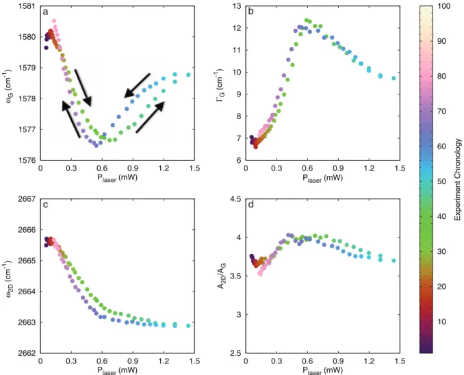
For the sample F1, Plaseris increased from 0.05 mW up to 1.5 mW and decreased back to 0.05 mW, as shown in
Figure 1. The G band at 1580 cm21for P
laser50.05 mW downshifts to reach a minimum value 1576.5 cm21for
Plaser50.5–0.6 mW. With the further increase of Plaser, it upshifts up to 1579 cm21(Fig. 1a). Correspondingly,
CGrises from 7 cm21up to 12 cm21for Plaser50.5–0.6 mW and then decreases to 10 cm21(Fig. 1b). In the same
SUBJECT AREAS: ELECTRONIC PROPERTIES AND DEVICES RAMAN SPECTROSCOPY CHARACTERIZATION AND ANALYTICAL TECHNIQUES OPTICAL PROPERTIES AND DEVICES Received 16 April 2013 Accepted 17 July 2013 Published 5 August 2013 Correspondence and requests for materials should be addressed to A.T. (Antoine.Tiberj@ univ-montp2.fr)
conditions, the 2D band continuously downshifts from 2666 cm21
down to 2663 cm21(Fig. 1c). The A
2D/AGratio displays a maximum
for Plaseraround 0.5–0.6 mW (Fig. 1d). The comparison of the
con-comitant evolution of vG, v2D, CG and A2D/AGwith electrostatic
gating results1–4indicates that the graphene doping is modified upon
light irradiation. In particular, the coincidence of the maxima of CG
and of A2D/AGwith the minimum of vGis a signature of neutral
graphene. The doping type is determined from the evolution of v2D3,4: a larger upshift for p-doping (below 0.5–0.6 mW) than for
low-level n-doping (above 0.5–0.6 mW). Interestingly, the changes are observed to be mostly reversible when Plaseris decreased back to
its initial value (Fig. 1). The doping of graphene deposited on a hydrophilic SiO2/Si substrate can be continuously and reversibly
tuned from the initial p-doping to quasi-neutral and eventually n-doping with moderate laser power. From the shifts and widths of the G band3,4, the inital doping of F1 was estimated to be p < 4 3
1012cm22at 0.05 mW. For P
laser 51.44 mW, the carrier density
was estimated to be n < 3 3 1012cm22. Similar observations were
made with different laser wavelengths: 488 nm, 514 nm and 660 nm (see Supplementary Figs. S3, S4, S5, and S6).
We now examine the influence of the underlying substrate by comparing these results to the ones obtained on sample F2 deposited on a less hydrophilic substrate and to sample F3 suspended over a trench etched into the substrate. The relative variations of the 2D and
G band positions as a function of Plaserare collected in Figure 2. This
particular representation disentangles doping and strain effects33. We
clearly observe three different behaviors in the plots presented on Figure 2. When the doping of graphene is continuously tuned from p-type to n-type, the 2D versus G positions presents the particular v-shape shown in Figure 2a. The G band consistently upshifts with an increasing charge carrier density (for both electrons and holes). The 2D band downshifts monotonically as the doping varies from p to n. Figure 2b displays the 2D vs G behavior for a flake lying on a less hydrophilic substrate. The G and 2D bands continuously upshift as Plaserincreases. The small upshift of the 2D band is expected for low
level n-type doping3,4,23. Here, C
Gis maximum for the lowest incident
power and continuously decreases with the increasing laser power, and so does the A2D/AGratio (see Supplementary Fig. S7 and S9).
Considered together, these variations indicate that this supported graphene is close to neutral for the lowest Plaserand becomes n-doped
as Plaseris increased (for Plaser52.6 mW, n < 4–5 3 1012cm22from
refs. 3 and 4). Once again, these doping variations are reversible when Plaseris decreased back. For the suspended graphene flake, F3, the
high values of CG(14 cm21) and A2D/AGratio (9.5) remain constant
through the entire power sweep (Supplementary Fig. S8). This indi-cates that F3 remains neutral as the laser power increases in agree-ment with S. Berciaud et al.35Thus, the small shifts of v
Gand v2D
(Fig. 2c) cannot be ascribed to any doping level variation.
1576 1577 1578 1579 1580 1581 0 0.3 0.6 0.9 1.2 1.5 a Plaser (mW) ωG (cm -1 ) 2662 2663 2664 2665 2666 2667 0 0.3 0.6 0.9 1.2 1.5 c Plaser (mW) ω2D (cm -1 ) 6 7 8 9 10 11 12 13 0 0.3 0.6 0.9 1.2 1.5 b Plaser (mW) ΓG (cm -1 ) 2.5 3 3.5 4 4.5 0 0.3 0.6 0.9 1.2 1.5 d Plaser (mW) A2D /A G Ex p eriment Chronolo gy 10 20 30 40 50 60 70 80 90 100
Figure 1|Reversible evolution of Raman spectra as a function of the incident laser power Plaserfor the graphene flake F1. (a) the G band position vG,
(b) the G band FWHM CG, (c) the 2D band position v2Dand (d) the integrated intensities ratio A2D/AG. The graphene flake F1 is exfoliated on a
hydrophilic substrate. Plaseris increased from 0.05 mW up to 1.5 mW and decreased back to 0.05 mW as shown by the arrows in (a). The color code of
each point corresponds to the chronological order in which the measurements have been carried out as depicted on the right hand side color bar (for the corresponding time see Supplementary Fig. S2).
We can now wonder whether these laser-induced doping varia-tions are uniform across the graphene surface. To this end, Raman mapping was performed at different laser powers on graphene exfo-liated onto a hydrophilic substrate and partially suspended over a pre-patterned trench (sample F4, see optical microscopy image in supplementary Fig. S1b where the mapped area is shown). Maps of the vG, CG, v2Dand A2D/AGare displayed on Figure 3 for seven Plaser
ranging from 0.1 mW to 3 mW. The constant position of the G and 2D bands across the whole supported area of the sample indicates that the strain and doping are homogeneous, therefore allowing to single out the influence of optical doping by the varying laser power. When the laser power is increased from 0.1 mW to 1.5 mW, the G band, initially at 1584 cm21 (C
G 5 7.5 cm21) shifts down to
1582 cm21 (C
G 512 cm21). Further increase of the laser power
inverts the effect and the G band upshifts back to 1583.5 cm21(C
G
decreases down to 9.5 cm21). For the same power sweep, the 2D band
continuously downshifts from 2676 to 2672 cm21. Similarly, the
A2D/AG ratio increases from 4.7 for Plaser 5 0.1 mW, to 5.1 for
Plaserbetween 0.5 and 1.5 mW, and then decreases back to 4.7 for
higher laser powers. These observations confirm that graphene sup-ported on hydrophilic SiO2evolves continuously from p-type to
n-type doped graphene when the laser power is increased.
Interestingly, the irradiation of the suspended graphene yields a very different behavior. Indeed, Figure 3 shows that both G and 2D bands downshift from 1581.5 to 1578.5 cm21 and from 2673 to
2663.5 cm21respectively as the laser power is increased. However,
CGand the A2D/AGratio remain constant (13 cm21and 5.9
respect-ively). Therefore the doping level remains unchanged through the entire power sweep and the downshifts of the 2D and G bands are ascribed to classical laser-induced heating effects that are also observed on sample F3 (see Supplementary Fig. S8, S11 and S12).
A careful examination of the signals recorded on the graphene edges and on the trench contour reveals that the optical doping is less effective in these specific locations. In particular, the doping
2662 2663 2664 2665 2666 2667 1576 1577 1578 1579 1580 1581 a F1 p i n ωG (cm -1) ω2D (cm -1) 2675 2676 2677 2678 2679 2680 1583 1584 1585 1586 1587 1588 b F2 i n ωG (cm -1) ω2D (cm -1) 2659 2660 2661 2662 2663 2664 1575 1576 1577 1578 1579 1580 c F3 i ωG (cm -1) ω2D (cm -1) Plaser (mW) 0 0.5 1 1.5 2 2.5 3
Figure 2|Comparison of the relative evolutions of the 2D band position (v2D) versus the G band position (vG) as a function of Plaserfor three graphene
flakes (F1, F2 and F3). F2 was exfoliated on a less hydrophilic SiO2/Si substrate than F1. F3 was suspended over a trench etched into the substrate.
The color code of each point corresponds to the incident laser power Plaseras displayed on the right hand side color bar. (a) F1 is p-doped at low Plaser, it
becomes quasi-neutral around 0.5 mW and n-doped for higher Plaser. (b) F2 is initially quasi-neutral and becomes n-doped with the increasing
Plaser. (c) The suspended graphene flake, F3, is neutral and stays neutral with the increasing Plaser. The measured shifts for F3 are only due to laser heating
effects. The different G band and 2D band positions (vG, v2D) of the different graphene samples (F1, F2, F3) in their quasi-neutral state are attributed to
strain fluctuations from one sample to the other.
2 μm 2 μm 0.1 mW 0.5 mW 1.0 mW 1.5 mW 2.0 mW 2.5 mW A2D / A G 4 5 6 ω2D (cm -1 ) 2664 2668 2672 2676 ΓG (cm -1 ) 8 10 12 14 3.0 mW ωG (cm -1 ) 1580 1582 1584
Figure 3|Raman maps measured for 7 different laser powers on sample F4. The rows correspond from top to bottom to the G band position vG, the
G band FWHM CG, the 2D band position v2D, and the integrated intensities ratio A2D/AG. The graphene flake is covering an etched pool of the
substrate that has a capsule shape and is visible on the right hand side of each map. The black upper left corners correspond to bare SiO2/Si surfaces. A
never reaches n-type even for the highest Plaser. We attribute this local
effect to the supplementary p-doping near graphene edges which has already been observed by Raman spectroscopy39,40.
Discussion
The absence of doping upon irradiation of suspended graphene clearly shows that the substrate contributes to the mechanism involved in the optical doping of graphene. We thus investigated the influence of substrate cleaning procedures on the efficiency of the optical doping. For highly hydroxylated (hydrophilic) substrates, freshly cleaned by O2plasma and/or piranha treatments prior to
graphene deposition, we observe the ambipolar behavior with a dop-ing evolvdop-ing from p-type to n-type upon increasdop-ing laser power. Our results confirm that graphene exfoliated on a hydrophilic substrate is p-doped41,42in contrast to the quasi-intrinsic state of suspended
gra-phene35. Across the different samples studied here, we found that the
Plaserfor which graphene is neutralized falls in the range 0.5–2 mW.
These values depend on the laser power density (laser spot size, see Supplementary Fig. S14) and graphene absorption (laser wavelength and SiO2thickness, see Supplementary Figs. S3, S4, S5, and S6). The
density of hydroxyl groups can be reduced by performing a thermal annealing of the samples under argon before graphene deposition. In this case, graphene was observed to be initially quasi-neutral and n-type doping was obtained upon illuminating the sample with increas-ing Plaser. Finally, when graphene is transferred onto substrates used
as-received without any cleaning, the doping of some flakes remain constant for all the entire Plaserrange (not shown). Therefore, the
absence of any significant spectral changes previously observed24
might be accounted for by the deposition of graphene on as-received substrates. Finally, it should be pointed out that the optical doping is not specific to graphene micromechanically exfoliated onto SiO2/Si
substrates but similarly occurs for graphene deposited on standard glass (not shown).
It thus appears that the starting value of the graphene doping level is directly linked to the substrate preparation. Cleaning procedures that render the substrate hydrophilic tend to result in more p-doped supported graphene, in agreement with previous studies43–47, which
also demonstrated the involvement of adsorbed water in the p-dop-ing of graphene by atmospheric oxygen36,42,45,47,48. Irreversible or slow
modulation of charge carrier density was demonstrated by changing the atmosphere36,42or by illuminating graphene with UV or visible
light36,37,49. In the latter cases, the invoked mechanisms relied on
dopant removal and more specifically oxygen derivatives. The char-acteristic times of such phenomena were found to be in the range of minutes36,49 or even hours37. Other authors have probed the
dynamics of charge transfer between the H2O/O2redox couple and
graphene by electrical measurements alone or combined with Raman spectroscopy. It was shown that the equilibrium is established after minutes48or hours42.
Our study shows that the charge carrier density can be conveni-ently tuned by adjusting the incident laser power even without a gating electrode. This effect does not involve the chemical modifica-tion of graphene since no D band emerges upon extended irradiamodifica-tion. By contrast with previous reports36,37,49, this laser-induced doping is
reversible with a characteristic time that was preliminarily evaluated to be less than 1 s (see Supplementary Fig. S15), i.e. orders of mag-nitude faster. This suggests that this phenomenon, although related to similar environmental effects, involves a different mechanism. O2
and H2O are playing a key role as illustrated by the weak dependency
of vGon Plaserfound after adsorbates removal by Ar annealing at
150uC of graphene lying on O2plasma treated SiO2/Si substrates34.
The transfer of ‘‘hot’’ electrons from optically excited graphene to the H2O/O2redox couple or O
{
2 superoxide anion proposed in reference
36 could only increase the hole doping in graphene upon visible light exposure, which is not supported by our observations. To get more insight on the underlying mechanism of the observed effect, we have
measured the evolution of the G-band Stokes/AntiStokes integrated intensity ratio as a function of Plaser(see Supplementary Fig. S11). We
were thus able to establish that, for graphene lying on a substrate, its local temperature increases by about 100uC/mW. This behavior was found to be similar for all the substrates tested (hydrophilic or less hydrophilic, 285 nm or 90 nm of SiO2). Considering the occurence
of a possible thermoelectric effect, the thermoelectric voltage that can build up in our experiments is expected to be of the order of few mV/ mW50, i.e. negligible when compared to the Fermi level shifts
mea-sured around 200 meV/mW. Furthermore, since the Seebeck coef-ficient is 0 for intrinsic graphene and since its sign changes with graphene doping type, the thermoelectric effect will tend to make the laser-exposed (hot) region evolve toward lower doping concen-tration. This is incompatible with our observations that the laser induces a doping type reversal for F1 (switching from p-type to n-type) and a n-type doping for F2, that was initially intrinsic. We thus tentatively attribute the observed effect to a local and reversible per-turbation of the chemical equilibrium between graphene, the sub-strate and the atmosphere by laser-induced heating. The fast dynamics and the reversibility of the effect cannot be related to dopant removal but can be compatible with a temporary destabiliza-tion of O{
2 species. Noteworthy, graphene lying on SiO2/Si exposed
to H2O alone, with only traces of O2, has been shown to be n-doped42.
Similarly, water significantly reduces hole doping of graphene depos-ited on mica51. The elucidation of the laser-assisted charge carrier
density tuning mechanism deserves further investigations which are beyond the scope of this paper.
In conclusion, we have shown that a low power visible laser light can be used to reversibly tune the charge carrier density of graphene lying on a substrate, with subsecond characteristic time. This effect is highly sensitive to the substrate hydrophilicity and completely sup-pressed in suspended graphene. The continuous tuning of the doping in graphene from p-type to n-type has been achieved on O2plasma
treated SiO2/Si substrates. The observed phenomenon is attributed to
a local and reversible perturbation of the chemical equilibrium estab-lished between graphene, the substrate and the atmosphere by laser-induced heating.
One technical implication of our study for the entire scientific community using Raman spectroscopy of graphene as a routine characterization technique is that it should be considered as poten-tially invasive as far as electronic properties are concerned. In par-ticular, the laser induced-modification of graphene doping could account for recent discrepancies between Raman and electrical trans-port measurements45. It would be interesting to extend the present
work to graphene on metals47and on silicon carbide52to assess how
carefully Raman experiments on graphene must be performed. On another hand, the ability to tune the charge carrier density with visible photons opens a wide set of opportunities to develop optically gated graphene electronic devices and a new approach to graphene optoelectronics. Finally, this effect should allow to study the interplay between graphene properties and the environment and to trigger laser-assisted functionalization of graphene leading to more advanced devices53,54.
Methods
Sample fabrication.Four samples (F1 through F4) were prepared. They consisted of a 500 mm thick highly p-doped monocrystalline Si (100) substrate, with a thermal oxide layer of 290 6 5 nm (in F1 and F3, oxide grown in O2; in F2 and F4, oxide grown in H2O) and a square matrix of metallic marks every 200 mm to ease the identification of graphene flakes. Samples F3 and F4 were further processed by etching matrices of 5 31 mm trenches with depths of 160 nm (F3) and 480 nm (F4) in between the metallic marks with a CF4ICP-RIE process.
Cleaning of F1 and F3 was performed by sonication in organic solvents (N-methyl-2-pyrrolidone, acetone and isopropanol; VLSI quality), immersion in piranha bath (H2SO4/H2O2351) during 3 hours and Ar/O2(351) plasma cleaning in a Fischione 1020 for 20 min. On the other hand, F2 and F4 were cleaned by sonication in organic solvents and O2plasma cleaning in a PVA TePLA 300 at 800 W for 15 min. In addition, sample F2 was annealed during 1 hour at 400uC in a 300 sccm Ar flow at atmospheric pressure.
The contact angles of deionised water on three Si (100) substrates with a 290 6 5 nm layer of thermal oxide (grown in H2O atmosphere) have been measured by the sessile drop method. Sample CA1 was only rinsed in water and dried in a N2flux to eliminate silicon particles resulting from cleaving, sample CA2 was cleaned using the same procedure as for F1 and F3 (i.e. piranha plus light O2plasma), and sample CA3 was cleaned as F2 and F4 (i.e. strong O2plasma). The resulting advancing quasi-static contact angles were 60 6 1u for CA1, unmeasurable or below 10u for CA2 and 18 6 1u for CA3.
Finally, graphene was deposited on all samples by exfoliation from kish graphite with the scotch tape method55.
Micro-Raman spectroscopy.Raman spectra were recorded using an Acton spectrometer fitted with a Pylon CCD detector and a 600 grooves/mm grating (, 2.5 cm21between each CCD pixel). The samples were excited with a 532 nm
(2.33 eV) CW frequency doubled Nd:Yag laser through a x100 objective (N.A. 0.9). The FWHM of the focused laser spot is 400 6 20 nm. At 1 mW laser power, the power density impinging on the sample is thus about 800 kW cm22(8 mW mm22).
Optimized focus conditions have been checked for each measurement. The samples are mounted on a three-axis piezoelectric stage to ensure the precise positioning and focusing of the laser spot. The maps were recorded with a 0.2 mm step in X (0.4 mm in Y) to probe the suspended graphene independently with a minimum of 2 to 3 points in the middle of the pool. The laser power was tuned with a variable neutral density filter controlled by a servomotor. The laser power was continuously measured by a calibrated photodiode put behind the beamsplitter. The whole experimental setup (spectrometer, piezoelectric stage, photodiodes, servomotor) were controlled by a dedicated and home-made Labview application. During laser power sweep or Raman mapping experiments, the acquisition times are varying from few seconds (2–5 s) at the highest power up to 30–60 s at the lowest power. The laser power sweep experiments typically last 20–60 min.
The results were reproduced on 8 hydrophilic samples (including F1 and F4, 3 others on 285 nm SiO2/Si and 3 on 90 nm SiO2/Si), 5 less hydrophilic substrates (including F2 and 4 on as-received SiO2/Si substrates) and 3 suspended graphene flakes (including F3 and the suspended part of F4). All the flakes have been measured on different locations and the measurements have been repeated several times. On most of the samples Raman maps at different laser powers have also been measured.
1. Pisana, S. et al. Breakdown of the adiabatic Born-Oppenheimer approximation in graphene. Nat Mater 6, 198–201 (2007).
2. Yan, J., Zhang, Y., Kim, P. & Pinczuk, A. Electric field effect tuning of electron-phonon coupling in graphene. Phys. Rev. Lett. 98, 166802 (2007).
3. Das, A. et al. Monitoring dopants by Raman scattering in an electrochemically top-gated graphene transistor. Nat Nanotechnol 3, 210–5 (2008).
4. Das, A. et al. Phonon renormalization in doped bilayer graphene. Phys. Rev. B 79, 155417 (2009).
5. Chen, C.-F. et al. Controlling inelastic light scattering quantum pathways in graphene. Nature 471, 617–620 (2011).
6. Mafra, D. L. et al. Using gate-modulated Raman scattering and electron-phonon interactions to probe single-layer graphene: a different approach to assign phonon combination modes. Phys. Rev. B 86, 195434 (2012).
7. Kalbac, M. et al. The influence of strong electron and hole doping on the Raman intensity of chemical vapor-deposition graphene. ACS Nano 4, 6055–6063 (2010). 8. Jung, N. et al. Charge transfer chemical doping of few layer graphenes: charge
distribution and band gap formation. Nano Letters 9, 4133–4137 (2009). 9. Zhan, D. et al. FeCl3-based few-layer graphene intercalation compounds: single
linear dispersion electronic band structure and strong charge transfer doping. Advanced Functional Materials 20, 3504–3509 (2010).
10. Bruna, M. & Borini, S. Observation of Raman G-band splitting in top-doped few-layer graphene. Phys. Rev. B 81, 125421 (2010).
11. Alzina, F. et al. Probing the electron-phonon coupling in ozone-doped graphene by Raman spectroscopy. Phys. Rev. B 82, 075422 (2010).
12. Zhao, W., Tan, P., Zhang, J. & Liu, J. Charge transfer and optical phonon mixing in few-layer graphene chemically doped with sulfuric acid. Phys. Rev. B 82, 245423 (2010).
13. Zhao, W., Tan, P. H., Liu, J. & Ferrari, A. C. Intercalation of few-layer graphite flakes with FeCl3: Raman determination of Fermi level, layer by layer decoupling, and stability. Journal of the American Chemical Society 133, 5941–5946 (2011). 14. Late, D. J. et al. Molecular charge-transfer interaction with single-layer graphene.
Journal of Experimental Nanoscience 6, 641–651 (2011).
15. Jung, N. et al. Optical reflectivity and Raman scattering in few-layer-thick graphene highly doped by K and Rb. ACS Nano 5, 5708–5716 (2011). 16. Zhang, Z., Huang, H., Yang, X. & Zang, L. Tailoring electronic properties of
graphene by p–p stacking with aromatic molecules. The Journal of Physical Chemistry Letters 2, 2897–2905 (2011).
17. Medina, H., Lin, Y.-C., Obergfell, D. & Chiu, P.-W. Tuning of charge densities in graphene by molecule doping. Advanced Functional Materials 21, 2687–2692 (2011).
18. Bruna, M. & Borini, S. Raman signature of electron-electron correlation in chemically doped few-layer graphene. Phys. Rev. B 83, 241401 (2011). 19. Howard, C. A., Dean, M. P. M. & Withers, F. Phonons in potassium-doped
graphene: the effects of electron-phonon interactions, dimensionality, and adatom ordering. Phys. Rev. B 84, 241404 (2011).
20. Singh, A. K. et al. Molecular n-doping of chemical vapor deposition grown graphene. J. Mater. Chem. 22, 15168–15174 (2012).
21. Crowther, A. C., Ghassaei, A., Jung, N. & Brus, L. E. Strong charge-transfer doping of 1 to 10 layer graphene by NO2. ACS Nano 6, 1865–1875 (2012).
22. Peimyoo, N., Yu, T., Shang, J., Cong, C. & Yang, H. Thickness-dependent azobenzene doping in mono- and few-layer graphene. Carbon 50, 201–208 (2012).
23. Parret, R. et al. In situ Raman probing of graphene over a broad doping range upon Rubidium vapor exposure. ACS Nano 7, 165–173 (2013).
24. Ferrari, A. C. et al. Raman spectrum of graphene and graphene layers. Phys. Rev. Lett. 97, 187401 (2006).
25. Poncharal, P., Ayari, A., Michel, T. & Sauvajol, J.-L. Effect of rotational stacking faults on the Raman spectra of folded graphene. Phys. Rev. B 79, 195417 (2009). 26. Lui, C. H. et al. Imaging stacking order in few-layer graphene. Nano Letters 11,
164–169 (2011).
27. Havener, R. W., Zhuang, H., Brown, L., Hennig, R. G. & Park, J. Angle-resolved Raman imaging of interlayer rotations and interactions in twisted bilayer graphene. Nano Letters 12, 3162–3167 (2012).
28. Kim, K. et al. Raman spectroscopy study of rotated double-layer graphene: misorientation-angle dependence of electronic structure. Phys. Rev. Lett. 108, 246103 (2012).
29. Martins Ferreira, E. H. et al. Evolution of the Raman spectra from single-, few-, and many-layer graphene with increasing disorder. Phys. Rev. B 82, 125429 (2010).
30. Venezuela, P., Lazzeri, M. & Mauri, F. Theory of double-resonant Raman spectra in graphene: intensity and line shape of defect-induced and two-phonon bands. Phys. Rev. B 84, 035433 (2011).
31. Eckmann, A. et al. Probing the nature of defects in graphene by Raman spectroscopy. Nano Letters 12, 3925–3930 (2012).
32. Mohiuddin, T. M. G. et al. Uniaxial strain in graphene by Raman spectroscopy: G peak splitting, Gru¨neisen parameters, and sample orientation. Phys. Rev. B 79, 205433 (2009).
33. Lee, J. E., Ahn, G., Shim, J., Lee, Y. S. & Ryu, S. Optical separation of mechanical strain from charge doping in graphene. Nat Commun 3, 1024 (2012). 34. Hulman, M., Halusˇka, M., Scalia, G., Obergfell, D. & Roth, S. Effects of charge
impurities and laser energy on Raman spectra of graphene. Nano Letters 8, 3594–3597 (2008).
35. Berciaud, S., Ryu, S., Brus, L. E. & Heinz, T. F. Probing the intrinsic properties of exfoliated graphene: Raman spectroscopy of free-standing monolayers. Nano Letters 9, 346–352 (2009).
36. Ryu, S. et al. Atmospheric Oxygen binding and hole doping in deformed graphene on a SiO2substrate. Nano Letters 10, 4944–4951 (2010).
37. Krauss, B. et al. Laser-induced disassembly of a graphene single crystal into a nanocrystalline network. Phys. Rev. B 79, 165428 (2009).
38. Mitoma, N., Nouchi, R. & Tanigaki, K. Photo-oxidation of graphene in the presence of water. The Journal of Physical Chemistry C 117, 1453–1456 (2013). 39. Zhang, W. & Li, L.-J. Observation of phonon anomaly at the armchair edge of
single-layer graphene in air. ACS Nano 5, 3347–3353 (2011).
40. Casiraghi, C. et al. Raman spectroscopy of graphene edges. Nano Letters 9, 1433–1441 (2009).
41. Casiraghi, C. Doping dependence of the Raman peaks intensity of graphene close to the Dirac point. Phys. Rev. B 80, 233407 (2009).
42. Levesque, P. L. et al. Probing charge transfer at surfaces using graphene transistors. Nano Letters 11, 132–137 (2011).
43. Lafkioti, M. et al. Graphene on a hydrophobic substrate: doping reduction and hysteresis suppression under ambient conditions. Nano Letters 10, 1149–1153 (2010).
44. Wang, R. et al. Control of carrier type and density in exfoliated graphene by interface engineering. ACS Nano 5, 408–412 (2011).
45. Nagashio, K., Yamashita, T., Nishimura, T., Kita, K. & Toriumi, A. Electrical transport properties of graphene on SiO2with specific surface structures. Journal of Applied Physics 110, 024513 (2011).
46. Lee, W. H. et al. Control of graphene field-effect transistors by interfacial hydrophobic self-assembled monolayers. Advanced Materials 23, 3460–3464 (2011).
47. Shin, D.-W. et al. A facile route to recover intrinsic graphene over large scale. ACS Nano 6, 7781–7788 (2012).
48. Xu, H., Chen, Y., Zhang, J. & Zhang, H. Investigating the mechanism of hysteresis effect in graphene electrical field device fabricated on SiO2substrates using Raman spectroscopy. Small 8, 2833–2840 (2012).
49. Luo, Z., Pinto, N. J., Davila, Y. & Johnson, A. T. C. Controlled doping of graphene using ultraviolet irradiation. Applied Physics Letters 100, 253108 (2012). 50. Zuev, Y. M., Chang, W. & Kim, P. Thermoelectric and magnetothermoelectric
transport measurements of graphene. Phys. Rev. Lett. 102, 096807 (2009). 51. Shim, J. et al. Water-gated charge doping of graphene induced by mica substrates.
Nano Letters 12, 648–654 (2012).
52. Sidorov, A. N. et al. Charge transfer equilibria in ambient-exposed epitaxial graphene on (0001–) 6H-SiC. Journal of Applied Physics 111, 113706 (2012). 53. Wang, Q. H. et al. Understanding and controlling the substrate effect on graphene
electron-transfer chemistry via reactivity imprint lithography. Nat Chem 4, 724–732 (2012).
54. Georgakilas, V. et al. Functionalization of graphene: covalent and non-covalent approaches, derivatives and applications. Chemical Reviews 112, 6156–6214 (2012).
55. Novoselov, K. et al. Electric field effect in atomically thin carbon films. Science 306, 666–669 (2004).
Acknowledgments
This work was supported by the french ANR (Grafonics project ANR-10-NANO-0004) and has been done in the framework of the GDRI GNT 3217 ‘‘Graphene and Nanotubes: Science and Applications’’. MR-R acknowledges Beatriu de Pino´s Marie Curie fellowship BP-0433 from AGAUR. A. Miranda is acknowledged for contributing to the design of substrates with trench arrays.
Author contributions
All authors (A.T., M.R.-R., M.P., J.-R.H., P.L., M.M., S.C., J.-L.S., E.D., A.-A.Z.) contributed extensively to the work presented in this paper.
Additional information
Supplementary informationaccompanies this paper at http://www.nature.com/ scientificreports
Competing financial interests:The authors declare no competing financial interests. How to cite this article:Tiberj, A. et al. Reversible optical doping of graphene. Sci. Rep. 3, 2355; DOI:10.1038/srep02355 (2013).
This work is licensed under a Creative Commons
Attribution-NonCommercial-NoDerivs 3.0 Unported license. To view a copy of this license, visit http://creativecommons.org/licenses/by-nc-nd/3.0