Deposition of Colloidal Quantum Dots by
Microcontact Printing for LED Display Technology
by
LeeAnn Kim
Submitted to the Department of Electrical Engineering and Computer
Science
in partial fulfillment of the requirements for the degree of
Masters of Engineering in Electrical Engineering and Computer
Science
at the
MASSACHUSETTS INSTITUTE OF TECHNOLOGY
February 2006
@
Massachusetts Institute of Technology 2006. All rights reserved.
Author.
... . . f ....Electrical Engineering and Comp. uter Science...Department of Electrical Engineering and Computer Science
January 2006
/I
Certified by...
/A Vladimir Bulovi6
Associate Professor, KDD Career Development Chair
SThesis Supervisor
A ccepted by ...
.:
: ..
,
·.
....
... ...
·
--
•Arthur
C. Smith
Chairman, Department Committee on Graduate Students
ARCHIVES
MASSACHUSETTS iMTmrTE.
OF TECHNOLOGY
AUG 14 2006
Deposition of Colloidal Quantum Dots by Microcontact
Printing for LED Display Technology
by
LeeAnn Kim
Submitted to the Department of Electrical Engineering and Computer Science on January 2006, in partial fulfillment of the
requirements for the degree of
Master of Engineering in Electrical Engineering and Computer Science
Abstract
This thesis demonstrates a new deposition method of colloidal quantum dots within a quantum dot organic light-emitting diode (QD-LED). A monolayer of quantum dots is microcontact printed as small as 20 4m lines as well as millimeter scale planes, and the resulting devices show quantum efficiencies as high as 1.2% and color saturation superior to previous QD-LEDs'. Through a modification of the polydimethylsiloxane (PDMS) stamp with a parylene-C coating, quantum dots solvated in chloroform were successfully inked and stamped onto various substrates, including different molecular organic layers. The ability to control the placement and the pattern of the quantum dots independently from underlying organic layers provides a new level of performance in QD-LEDs, increasing the possibility of QD-LED displays.
Thesis Supervisor: Vladimir Bulovid
Acknowledgments
I would like to thank everyone I have worked with in LOOE. Vladimir BuloviP has been a supportive and creative advisor and I am lucky to have meandered my way into his lab. I am indebted to Seth Coe-Sullivan for being the mentor who guided me through the first year of research in a completely new field to me. Some of the work shown here is his work, and is a result of how meticulous a scientist he is.
I have a special thank you for Polina Anikeeva. All of the tribulations of working with quantum dots, she went through with me. More importantly, she is a spunky, intelligent woman I respect and I've learned a lot from her. Some of the work here is also hers.
I thank both Scott Bradley and Gerry Chen for being very good officemates
-fun to talk to, good to collaborate on homework with. Conor Madigan for his hu-mor, braininess (neuroticism), and procastinations. John Kymissis for his all around knowledge of anything practical. Ivan Nausieda for TRL help and having character. I'd like to thank Jen Yu for also being a woman I really respect and who has tons of character (marry me!). Additionally, Yaakov Tischler with his enthusiasm, John Ho by being the nice guy, Vanessa Wood with her energy and Ethan Howe with his singing have made it a pleasure to work with this lab. And I'd like to mention Ryan Tabone for suffering stamping with me and being a good listener.
I'd like to thank Alexi Arango for many things, as much within the lab as without. Finally, I'd like to thank my friends. The best brother, Andrew. The best person on earth sister, SueAnn. And my mother and father, Eunjoo and Ducksoo Kim, for their love and supporting me all the way.
Contents
1 Introduction 15
2 Displays 17
2.1 Human Visual Perception ... . . . . 17
2.1.1 Color ... ... .. 17
2.1.2 Spatial Response: Resolution . ... . 21
2.1.3 Temporal Response: Refresh Rate . ... . 22
2.2 Present Technology ... ... 22 2.2.1 CRT ... ... ... ... 22 2.2.2 LCD ... ... .... ... ... 23 3 QD-LED Background 25 3.1 LED ... ... ... ... 25 3.2 OLED ... ... ... ... 26 3.3 QD-LED ... ... ... ... 27 3.3.1 Quantum Dots ... ... 27
3.3.2 Hybrid Inorganic/Organic Device . ... 29
3.3.3 Deposition of Monolayer QD Film . ... . 31
4 Printing and Patterning Background 35 4.1 Traditional Methods ... ... ... . 35
4.1.1 Lithography ... ... . 36
4.1.2 Relief and Intaglio ... .. . . 37 7
4.1.3 Silkscreen ... 4.2 Soft Lithography ... 4.2.1 Background ... 4.2.2 Microcontact Printing 4.2.3 Microtransfer Molding 4.2.4 PDMS ... 5 Stamped QD Films
5.1 Background: Phase Separation . . . . 5.2 Microtransfer Molding (Micromolding) . 5.3 Improving Surface Kinetics of the Stamp
5.3.1 Surface Wetting . . . . 5.3.2 Surface Energy ...
5.3.3 Low Surface Energy of PDMS . .
5.3.4 Improving Interfacial Energy . . . 5.4 Microcontact Printing ...
6 Device
6.1 Device Performance . . . . 6.1.1 I-V and Quantum Efficiency . . . 6.1.2 Color . . . . 6.2 Patterned Devices . . . . 7 Conclusion 45 . . . . . 45 . . . . . 46 . . . . . 48 . . . . . 48 . . . . .. 5 1 . . . . . 54 . . . . . 54 . . . . 56 63 63 63 65 67 79
List of Figures
2-1 Electromagnetic spectrum. [1] ... ... 18
2-2 CIE diagram which maps any XY coordinate calculated from a spectral distribution onto a distinct perceived color. Approximation of the color regions are shown and not a representation of the true color. ... 19
2-3 Multiplying each sensitivity curve above with the spectral distribution of the light source, integrating the results and normalizing all three values to add to 1, will give the X, Y and Z values corresponding to CIE coordinates. It should be noted that these curves are not the same as the actual sensitivity curves of the cones. They have been modified
for practical modelling reasons. ... 20
2-4 Sinusoidal pattern used to determine the spatial limit of the human eye. [2] . . . .. . 21
2-5 Schematic of a cathode-ray tube, the bulky standard television display. [3] 23
2-6 Schematic of the liquid crystal display. [4] . ... 24
3-1 A heterojunction organic device, which contains two organic layers, of which at least one exclusively transports a single type of charge. This
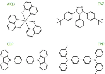
3-2 Typical small-molecule organics. Tris-(8-hydroxyquinoline) aluminum known as Alq3. 3,5-Bis(4-tert-butyl-phenyl)-4-phenyl-[1,2,4]triazole known as TAZ. 4,4'-Bis(carbazol-9-yl)biphenyl known as CBP. N,N'-Bis(3-methylphenyl)-N,N'-bis-(phenyl)-benzidine known as TPD. CBP and TPD are hole transporters and AlQ3 is an electron transporter, while
TAZ acts as a hole blocker. The AlQ3 is often also the luminescent layer. 27 3-3 Absorption spetra of CdSe QDs, size tuned from 12 to 115 A. [5] . . . 28 3-4 a) Structure of core-shell quantum dot, with organic capping. b)
Var-ious cappings for quantum dots, such as oleic acid, trioctylphosphine oxide, and pyridine. The most common capping on the quantum dots
for this work are TOPO... ... 29
3-5 An OLED with a single monolayer of well-ordered quantum dots placed at the interface between the hole transporting layer and the hole
block-ing layer... ... 30
3-6 Thermal evaporation chamber, in which current runs through a boat holding the desired material to be deposited. As the resistive boat heats up, the material sublimes and condenses when it hits the substrate above. 31 3-7 Spincasting procedure and phase separation principles form the
well-ordered quantum dot film atop TPD. . ... 32
3-8 AFM of monolayer of well-packed quantum dot atop organic molecule T P D .. . . . . .. . . . .. .. 33 4-1 Photolithography which is the mainstay of the microelectronics
indus-try is used for patterning silicon as well as other semiconductors and
metals. ... . . . ... ... . 36
4-2 Relief and intaglio printing. ... 37
4-3 Shadowmasking to pattern thermally evaporated organic layers. ... 38
4-4 Procedure for casting patterned PDMS stamps from silicon masters.. 40
4-5 PDMS conformally contacts substrates on both the micro and macro
4-6 Examples of microprinted structures. [6] . ... 41
4-7 Examples of micromolded structures [6]. . ... 42
4-8 PDMS molecular structure[6]. ... 43
4-9 Curing mechanism of PDMS and resulting cross-linked elastomer. [7] 44 5-1 Printed quantum dot film from spincasting on a flat PDMS stamp. 47 5-2 Photoluminescence optical microscope photo of a film printed by spin-casting on a smooth surface of PDMS. Nonuniformity is visible on the m icron scale. ... . 48
5-3 AFM of molded quantum dots in a period pattern of circles. ... 49
5-4 AFM of the silicon masters from which the stamps were made... 49
5-5 Contact angle of a chloroform droplet on PDMS ... 50
5-6 Contact angle of a water droplet on PDMS as a reference point. . .. 50
5-7 Intermolecular forces balance out in the bulk of a liquid. But at the surface, lack of neighboring molecules cause an imbalance and greater forces between the molecules present. . ... . . 51
5-8 The lower the contact angle, the better the liquid is said to wet the substrate. . .. . . . .. 52
5-9 Figure of the different surface areas. ... ... 53
5-10 Oxygen plasma and UV ozone treatments make the surface of PDMS have a higher surface energy because of the chemically reactive OH groups.. . . . ... . . 55
5-11 Photoluminescence optical microscope photo of a film printed by spin-casting on a an oxygen plasma treated PDMS surface. Nonuniformity is visible on the micron scale . . . . . 56
5-12 Contact angle of a chloroform droplet on parylened PDMS. ... . 57
5-13 Molecular structure of parylene-C. ... .. 57
5-14 Microcontact printed film of CdSe quantum dots on CBP. . ... 59
5-15 Partial monolayer microcontact print of QDs on CBP ... . 59 5-16 Partial monolayer microcontact printed film of quantum dots on TPD. 60
5-17 Partial monolayer microcontact printed film of quantum dots on Silver. 60
5-18 Microcontact printing of 60pm large circles. . ... 61
5-19 Close-up AFM of the circle. ... 61
6-1 Device with microcontact printed red QD film, showing good large area uniformity and coverage on the scale of the device. The blue spot in the lower corner shows a defect in the stamped QD film, allowing the
organic TPD emission to be seen. ... 64
6-2 IV curves for LEDs that contain stamped QD films, with colors
corre-sponding to that of QD emissions ... 65
6-3 Quantum efficiency curves for LEDs that contain stamped QD films, colors corresponding to that of QD emissions. Phase separated QE
curves shown as dotted lines ... 66
6-4 Spectra curves for devices that contain stamped QD films. ... . 67 6-5 CIE coordinate comparison between stamped and spun devices, and in
relation to the NTSC triangle ... 68
6-6 Electroluminescence of a patterned green QD-LED device correspond-ing to the AFM shown in Fig. 5-18 Device is 1mm in diameter.... .. 69 6-7 AFM of the QD circles patterns, offset to show the area between circles. 69 6-8 Deformation of patterned PDMS that resulted in the QD film shown
in Fig. 6-7 due to elastomeric quality of the stamp. . ... 70 6-9 1mm diameter device showing red quantum dots patterned in stripes.
Organic emission visible at a higher operating current, in the
right-hand photo . ... . ... . 71
6-10 A 10 pm line pattern corresponds to a resolution of about 850 dpi for a three color system. The numerous defects are associated with various problems of packaging and isolation from abient conditions. ... 72 6-11 Green quantum dot lines printed on red quantum dot lines. ... . 73
6-12 Electroluminescence spectra of the device shown in Fig. 6-11. The TPD peak ceneters roughly around 415 nm, the green at 525 nm, and
the red at 615nm ... ... 74
6-13 AFM of a line of green quantum dots on top of a line of red quantum
dots. ... .. 75
6-14 Photoluminescence of red quantum dot lines, showing the pronounced edge effect .. . . . .... . . . .. . 75 6-15 First three bottom layers in the device being operated in Fig. 6-16 and
Fig. 6-18. . . . .. . . . .. . . .. . . .. . 76 6-16 Lines of red quantum dots printed atop a full-plane green quantum
dot film. An area where the PDMS did not contact the substrate when printing the green QDs shows the red QD emission as well as the organic. However, in all other areas, the luminescence of the red dots
is much reduced. ... 77
6-17 Cartoon showing that it would seem relaxation and luminescence is en-ergetically favored to occur on the red QD film. Instead green emission
is favored. ... 77
6-18 The same device as Fig. 6-16 except the green QD coverage is com-plete. The corresponding spectrum of this device is shown in Fig. 6-19 showing indeed there is very little red emission. . ... . . 78 6-19 Spectrum of the device shown in Fig. 6-18, which shows minimal red
Chapter 1
Introduction
An organic light-emitting diode, also known as an OLED, is an emerging display technology. As information continues to become densified, manipulated, and traded at rates faster than ever, the visual medium has become critical and technologically sophisticated. From televisions to computers, music players and cameras, it is difficult to avoid displays. There always seems to be a demand for displays that trump the current best. More color, more light, better detail. Recently, OLEDs that incorpo-rated a new type of material, called quantum dots (QDs), demonstincorpo-rated the potential to improve OLED display performance.
OLEDs consist of organic layers that transport electrons from the cathode and holes from the anode, to create excited state electron-hole pairs called excitons. These excitons relax on a molecular site and emit light. When quantum dots are included in the organic layers, some of the exciton relaxation occur on the dots, resulting in light characteristic of the quantum dot. Emission from quantum dots is notable, in particular because its color-tunability and color purity far exceed that of organic molecules. A recent demonstration of a new QD-LED device architecture showed the possibility of having most of the light emission occur from the quantum dots, as opposed to from the organics. The placement of a monolayer of quantum dots, at the correct interface between two organic layers, results in an efficient and superior color device. However, the method employed to generate such a monolayer does not allow for the patterning of pixels required for displays. It also introduces impurities
through solvent exposure.
This thesis continues the work of QD-LEDs by developing a device-compatible quantum dot deposition technology. It explores the possibility of microcontact print-ing as a way to pattern the quantum dot monolayer film and protect the underlyprint-ing organic layer from degradation. A brief discussion is presented on other patterning techniques that are used in both the traditional printing field and within the organic field. The issue of obtaining a well-formed monolayer film by microcontact printing is then addressed and, through use of surface control, the desired film is achieved and patterned into devices.
Chapter 2
Displays
The purpose of an electronic display is to communicate information to people through images. Its design is therefore determined by how a viewer receives and interprets optical signals. We begin with a discussion on how colors are perceived, and the spatial and temporal acuity of the human visual system.
We then discuss two of the most dominant display technologies that are currently in use, the cathode ray tube (CRT) and the liquid crystal display (LCD).
2.1
Human Visual Perception
2.1.1
Color
The visible part of the electromagnetic wave spectrum covers from 770 nm to 380 nm, red to blue. It is a very narrow slice of the EM specrum, to which human eye receptors have a special sensitivity. The eye is made up of two types of light receptor cells - cones and rodes - which lie on the retina, the innermost layer of the eyeball. The rods are luminosity sensors, and relay only grayscale information about
luminance levels. Cones can differentiate between different wavelengths of light, for the perception of color. There are three different subtypes of cones: short-wavelength cells peak around 440 nm, medium at 540 nm, and long at 565 nm. These cones work together to interpret a spectral distribution in form of a perceived color [2].
0(I- n m I10- 1 nm1 10-4 nm 10--' nm t1-' nm I nm 10 nm I00 nmn 10 111nm = I pmi 10 pm 100 Pim 10i)mm = I cm it) cm 100 cm = I m 10 m 1001 m 100l) ti = I km (10 km 100 km Violet Bluc Green Yellow Orangc Red radiatlon ) waves
I
0.91
Aooroxirnate Color Reaoons on
4low
Snrn
o
0 0.1 0.2 0,3 0.4 0.5 0.6 0.7 0.8 X
Figure 2-2: CIE diagram which maps any XY coordinate calculated from a
spec-tral distribution onto a distinct perceived color. Approximation of the color regions are shown and not a representation of the true color.
Different spectral distributions can be perceived as exactly the same color. For instance, the combination of a red and green light will produce the sensation "yellow", as would a spectrally pure monochrome light with a wavelength of 600 nm. In 1931, the Committee International de l'Eclairage developed a useful model for the spectral sensitivity of the cones (Fig. 2-3). By using these curves and the spectral distribution of light entering the eyes, a set of three values are obtained that uniquely define the color interpreted by the eye-brain system. The CIE chromaticity diagram charts these coordinates (Fig. 2-2).
The edge of the CIE diagram represents pure colors. These edges can only be attained by single wavelength electromagnetic radiation, and their combination can give any color within the horseshoe shaped boundary of the chart they define. If three points are chosen on the CIE diagram, the colors within the triangle defined will be producible by a weighted mixture of those three colors corresponding to the corners. The conclusion is then that the more saturated the colors of the corners are,
r-_ t tj
1.8- 1.6- 1.4- 1.2- 1.0- 0.8- 0.6- 0.4- 0.2-0.0 0.2
-Z
SI * I * I * I * I 300 400 500 600 700 800 Wavelength [nm]Figure 2-3: Multiplying each sensitivity curve above with the spectral distribution
of the light source, integrating the results and normalizing all three values to add to 1, will give the X, Y and Z values corresponding to CIE coordinates. It should be noted that these curves are not the same as the actual sensitivity curves of the cones. They have been modified for practical modelling reasons.
Figure 2-4: Sinusoidal pattern used to determine the spatial limit of the human
eye. [2]
the wider the range of attainable colors. A saturated light source is characterized by a very narrow linewidth emission spectrum.
2.1.2
Spatial Response: Resolution
The ability to discern details is called visual acuity, and it is often measured by determining the smallest distance in which change of luminance or color is detectable by the human eye. It is undersirable for a viewer to be able to discern pixilation of an image on a display screen. The illusion of spatial continuity that mimics how people see the actual world is important to users of electronic displays, for practical and emotional reasons. If given a sinusoidal pattern of alternating dark and light lines (Fig. 2-4, the human eye will be at the limit of visual acuity at the frequency those lines indistinguishably merge. Visual acuity peaks at approximately 10-30 cycles per visual degree, and is generally assumed to reach a limit around 50-60 cycles per visual degree. This upper limit translates to roughly 300-600 dots per inch, or around 85pm
- 42pm large pixels (where a pixel is three subpixels of red, green, and blue). To make a display with a resolution that exceeds this specification would provide no gain because of the physiological limit of the eye.
2.1.3
Temporal Response: Refresh Rate
Human eyes take in information at a finite rate. Even though it seems like we view the world in a continuous fashion, in actuality the eye takes in discrete "snapshots" which the brain processes into one continuous motion. This is because it takes time for receptors to respond, signals to be sent to the brain, and the receptors to reset in preparation for the next set of signals. This property of the human visual system allows quick succession of frames to be seen as one fluid motion, and an electronic display only needs to show a succession of still frames at a fast enough rate to emulate smooth motion. However, the rate varies because the eye is sensitive to change in illumination intensities, so movies played in a dark theatre are played at 24 frames/s, while televisions refresh at a rate of 50 or 60 images per second. If this rate is too slow, not only does the motion look unrealistic, but the luminance also appears inconstant resulting in a "flicker" effect. To avoid this flicker, a display needs to refresh in the range of 60-85 cycles per second.
2.2
Present Technology
2.2.1
CRT
The cathode ray tube technology is more than 100 years old. It is the cheapest display form and still maintains a prevalent position. One of the last widely used application of the vacuum tube, the CRT works by shooting an energetic beam of electrons at a screen of different colored phosphors. This beam can be bent and directed at different parts of the screen, illuminating any one point of the complete image. The standard scheme to produce a whole image is to have the beam scan each horizontal line, starting from the top and moving to the bottom. Done quickly enough, the viewer sees one complete frame, and if the frames are updated quickly enough, one fluid motion.
The advantages of the CRT are that it is a mature and cost competitive technology. In almost all areas, including color, viewing angles, resolution, brightness, and speed,
ight itput
Figure 2-5: Schematic of a cathode-ray tube, the bulky standard television dis-play. [3]
the CRT performs very solidly. However, its size has been a primary drawback that has motivated the unrelenting development and refinement of flat-panel displays. Because of the vacuum tube, a CRT display is bulky in terms of depth, and also heavy. It is not readily portable nor easily insertable into many applications that require a display.
2.2.2
LCD
The liquid crystal display (LCD) uses the property that liquid crystals can exist in different phases, some more ordered than others depending on temperature, and can be made to align through a field effect. By applying a voltage across the liquid crystal, the light that reaches the viewer can be modulated between off and on, sometimes with the additional use of a polarizing sheet. One scheme is shown in Fig. 2-6. For color LCDs, the light that passes through the liquid crystals is then passed through red, green, and blue filters.
LCDs are the dominant flat-panel display at the moment. They appear in many different applications, most familiarly in laptops and digital camera viewfinders. How-ever, they show weaknesses in several areas that have prevented penetration into large surface area and video applicaitons. Viewing angles are narrow compared to other display technologies. Color range is underwhelming, and power efficiency is lowered because of the use of filters. Switching speeds between off and on states are in the
Figure 2-6: Schematic of the liquid crystal display. [4]
milliseconds due to LC effects as well as the crystals themselves requiring time to respond. For high-quality video, LCD's slow response time produces artifacts such as blurring and choppiness. Finally because of the layered complexity, manufacturing of LCDs is hard to make cost effective.
Chapter 3
QD-LED Background
Alternatives to CRTs and LCDs, the two dominant display technologies, exist. An example is the plasma display, which is an expensive, high definition, thin-form alter-native to the CRT television screen. Another example, the subject of this work, is the organic light-emitting diode (OLED). In this section, we discuss the more traditional inorganic light emitting diode (LED), the newer organic LED, and then a variation upon the organic form that uses quantum dots.
3.1
LED
The inorganic light-emitting diode, simply referred to as an LED, emits light by passing current through an emissive layer. Recently, LEDs have been showing up in direct-viewing applications such as traffic lights and indicator lights, but not as much in full-color displays for television and monitors. One of the main reasons for this is the cost of fabricating LEDs. The most simplistic version is a dual single-crystal semiconductor epitaxially grown to form a p-n junction. High quality epitaxial growth is an expensive, slow process. However, it is an inherently thin form device. In addition, LEDs have superior viewing angles and better power usage because of the lack of filters that absorb some of the light emissions. Yet, due to fabrication requirements, superior LED efficiencies, colors, and viewing angles are not enough to compete with the popularity of LCDs.
3.2
OLED
Organic light-emitting diodes could address this missing element of easy, cheap manu-facturability while maintaing the potential for superior color and brightness, contrast, power efficiency, as well as fast time responses, wide viewing angles, and simplified manufaturability [8]. Organic semiconductors were recognized as potential electro-luminescent lumophores over fifty years ago. But problems such as instability and low-carrier mobilities made organic light-emitters elusive [9]. The earliest reports of electroluminescence (EL) from organic materials used very thick films of anthracene and had operating voltages in the hundreds of volts [10] [11]. It took another twenty years until Ching Tang demonstrated a reasonable device that operated at less than 10V through the use of a new device structure [12][13]. With the demonstration of polymer organic devices by Burroughes et al. [14] a few years later, the work touched off the field of organic LEDs.
ITO Glass
Figure 3-1: A heterojunction organic device, which contains two organic layers,
of which at least one exclusively transports a single type of charge. This effectively determines where excitons are formed.
Tang's OLED consisted of a heterojunction of two relatively thin organic layers, one capable of transporting only one type of charge. Present day OLEDs, which still make use of this multi-junction architecture, continue to make improvements in quantum efficiences, color, and lifetime. While they are viewed as a serious alter-native to other light technologies, to date they have appeared mostly in smal-scale,
short lifetime applications, such as camera displays and cellphone indicators and dis-plays. They have yet to achieve performance numbers that are convincing of their competitiveness in the large-display industry.
TAZ
CBP TPD
/
Figure 3-2: Typical small-molecule organics. Tris-(8-hydroxyquinoline) aluminum
known as Alq3. 3,5-Bis(4-tert-butyl-phenyl)-4-phenyl-[1,2,4]triazole known as TAZ.
4,4'-Bis(carbazol-9-yl)biphenyl known as CBP. N,N'-Bis(3-methylphenyl)-N,N'-bis-(phenyl)-benzidine known as TPD. CBP and TPD are hole transporters and AlQ3
is an electron transporter, while TAZ acts as a hole blocker. The AlQ3 is often also
the luminescent layer.
3.3
QD-LED
3.3.1
Quantum Dots
Quantum dots are nanoscale semiconductor spheres that exhibit properties deviating from that of the bulk due to quantum confinement. As a nanocrystal shrinks in size and becomes smaller than the bulk exciton diameter, the HOMO and LUMO gap widens and the emission is blue-shifted. Precise control over the wavelength of emission is given by a straightforward selection of crystallite size [15], while using the same basic synthetic procedure. Because of the discretization of the density of
states at the band edge, emission becomes narrowed due to quantum confinement. A typical photoluminescence FWHM is 30nm or less. This spectral narrowing is important because it is an indication of the color purity of emitted light. As shown before with the CIE diagram, the more saturated the set of base mixing colors, the more extensive the full palette is.
C
a
300 350 400 450 500 550 600 650 700 750
Wavelength (nm)
Figure 3-3: Absorption spetra of CdSe QDs, size tuned from 12 to 115
A.
[5]The quantum dots that are used in this work are colloidally grown core/shell quantum dots with a passivating organic capping group. At the surface of the quan-tum dot, the crystallinity of the semiconductor is interrupted because of the lack of the appropriate number of neighboring molecules. The surface states act as traps that provide for nonradiative recombination, which lowers the efficiency of the dots. By epitaxially growing a shell layer of a wider bandgap semiconductor material, the quantum dot surface can be passivated [16]. A prime example is a CdS coated CdSe quantum dot [17]. The final layer of organic capping allows the quantum dots to be solvated in organic solvents, and therefore processable much in the same manner as
organic molecules. The organic cappings also prevent aggregation and precipitation of the quantum dots. Some common organic cappings include oleic acid, pyridine, trioctylphosphine oxide, and thiols.
a.)
'0·~;
X
b.) (H2C)7H3C (CH2)7COOH I \ H H Oleic Acid N Pyridine TOPOFigure 3-4: a) Structure of core-shell quantum dot, with organic capping. b) Various cappings for quantum dots, such as oleic acid, trioctylphosphine oxide, and pyridine. The most common capping on the quantum dots for this work are TOPO.
Using CdSe QD as an example, the colors that can be attained by tuning range from 1.7 eV which corresponds to the bulk, and a wavelength in the far red of 730 nm, to 2.75 eV which corresponds to a blue wavelength of 450 nm [5]. Capable of accessing this wide range of colors, exhibiting narrow linewidths, and being made up of inorganic materials that are potentially more stable against oxidation compared to organic molecules, the quantum dot may be the ideal, alternative lumophore to enhance OLED performance.
3.3.2
Hybrid Inorganic/Organic Device
OLEDs that contain quantum dots as the lumophore are referred to as QD-LEDs. In 1994, Vicki Colvin et al. fabricated a hybrid polymer/QD-LED displaying prominent
QD electroluminescence characteristics with external efficiences between 0.001% and 0.01% [18]. In 2002, Seth Coe et al. demonstrated a QD-LED with a peak quantum efficiency of 0.52% [19], and have continued to improve the efficiencies. Those devices incorporate only a monolayer of quantum dots as the luminescent layer inbetween organic layers. They show high brightness and small spectral FWHM, and the tech-nique for making such devices was shown to be applicable to a wide range of particle materials, dimensions, and shapes [20]. These improvements were attained by a de-vice architecture in which the quantum dots were physically isolated to a well-ordered monolayer between the organic layers.
T-er of Quantum Dots
ITO
I I Glass
Electron Transport Layer
Hole Blocking Layer
-Hole Transport Layer
-
et-th +
Figure 3-5: An OLED with a single monolayer of well-ordered quantum dots placed at the interface between the hole transporting layer and the hole blocking layer.
The monolayer sandwich structure drastically improves the QD-LED quantum efficiency because charge transport isn't hindered by highly resistive quantum dots. The organic semiconductors act as the hole and electron transport layers, electron-hole pairs called excitons form near or on the quantum dot, and then those excitons
relax within the dots resulting in radiative emission. In this manner, the ratio of quantum dot emission to organic emission is dramatically increased allowing for the device light output to be almost solely defined by the quantum dot.
3.3.3
Deposition of Monolayer QD Film
Small molecule organic film deposition is most commonly done by thermal evapora-tion techniques in high vacuum environments. In contrast, deposievapora-tions of polymeric molecules use methods such as dip-coating or spin-casting out of solution. Both types of organics and respective deposition methods present advantages and disadvantages, but for quantum dots, thermal evaporation is not an option because of their size, weight, and composition. Before the monolayer device, QD-LED devices were made by spin-casting a thick layer of quantum dots on top of a polymer layer such as
PPV [18][21].
vra n ilm -hmhm r
Figure 3-6: Thermal evaporation chamber, in which current runs through a boat holding the desired material to be deposited. As the resistive boat heats up, the material sublimes and condenses when it hits the substrate above.
The monolayer films are formed by spin-casting quantum dots, while also utilizing the principle of phase separation. A chloroform solution of small molecule organic and quantum dots are spin-cast at appropriate concentration and spin parameters,
resulting in the quantum dots rising above the layer of small molecule organics in a neat hexagonally close packed film.
I1. solution of quantum dots/TPD/chloroform
2. dropped onto a substrate, which is then spun
3 spinning dries the solution as weli as spreads it our and phase separates the quantum dots trorn TPD
4. leaving behind a thin film of TPD layered below a thin film of quantum dot
spin
C
i, ..- JFigure 3-7: Spincasting procedure and phase separation principles form the
well-ordered quantum dot film atop TPD.
Figure 3-8: AFM of monolayer of well-packed quantum dot atop organic molecule TPD.
50nm
I
Chapter 4
Printing and Patterning
Background
A QD-LED display requires devices that are small enough to meet the requirements of the human visual system, and these devices must be placed next to each other in a precise and regular layout. Just like the optical lithographic methods in the mi-croelectronics industry that produces chips of tiny components with high throughput and precision, these displays need a patterning technique. Ultimately, this work will focus on a microcontact printing method to achieve patterning capability.
This section gives background on traditional printing and patterning methods. We then review the concepts of microcontact printing and microtransfer molding, since these two patterning techniques are further discussed in the experimental chapter.
4.1
Traditional Methods
The invention of printing is an important milestone in the history of civilization. It is a communication technology that mass reproduces and distributes ideas over distance and time. Printing techniques have traditionally fallen into four main categories: relief, intaglio, lithography, and silkscreen. Modern advances have created other that do not fit comfortably into these categories of stamp and substrate, including those of electrophotography (xerography) and ink-jet printing [22].
4.1.1
Lithography
It is interesting to start with lithography because of its familiarity to the semicon-ductor industry. A planographic (flat-surfaced) process, the image is set on a level surface without incisions and contour changes [23]. In the original instantiation of lithography, the image was drawn on a smooth-faced stone in a greasy substance and then the whole stone was dampened with water. The ink rolled onto this stone had an affinity for the greased areas while simultaneously repulsed by the areas covered only by water. In this way a copy of the image in ink could then be transferred to a piece of paper.
expose photoresist to light through mask
Photoresist latent image in photoresist
Substrate
Remove photoresist Etch substrate Remove photoresist
1
II-
I.
Figure 4-1: Photolithography which is the mainstay of the microelectronics in-dustry is used for patterning silicon as well as other semiconductors and metals.
Lithography in microelectronic device manufacturing is planographic but different in that the image is placed onto the surface (usually that of photoresist) by illumi-nation by light through a mask. The image resides latently in the photoresist, which has reacted to the exposure of light. Subsequently, the photoresist is developed and washed away, leaving either the positive or negative image of the mask. Once this photolithography is performed, the exposed underlying substrate may be selectively
etched due to the protection of the patterned photoresist.
4.1.2
Relief and Intaglio
In contrast, relief and intaglio printing rely on raised and sunken surfaces. Relief printing uses a template in which the desired image extends out from the surface. This template is inked and then pressed against the paper, or desired substrate, and only the extruded areas leave an imprint. Intaglio is the exact reverse, in which the image is dug into the template, etched chemically or physically. These recesses are filled with ink, while the flat surface stays clear of ink, so upon transfer the image is defined by the grooves [23].
Relief Intaglio
nK
resulting prints
Figure 4-2: Relief and intaglio printing.
4.1.3
Silkscreen
Silkscreen is the method by which ink is pushed through a screen, blocked in places by a stencil in the screen. This method is noteworthy here in that it is similar in principle to shadowmasking. Small-molecules organics, as opposed to polymers, are deposited by thermal evaporation and can be patterned by placing a "stencil" between
i--I=
the source and the substrate. The stencil is called a shadowmask, and is usually made of metal, placed in contact mode with the substrate.
CkhS A M. a 1
Substrate with patterned
organic material
Figure 4-3: Shadowmasking to pattern thermally evaporated organic layers.
4.2
Soft Lithography
4.2.1
Background
Optical lithography, or photolithography, is the most essential, fundamental technique of microfabrication. Almost all integrated circuits are fabricated using photolithogra-phy. Nevertheless, there are limitations to photolithography, such as being expensive, poorly suited for nonplanar surfaces, and applicable mainly to just photoresists also motivate the exploration of something like microcontact printing [24]. In our case, the need to work with nontraditional materials is a central reason for pursuing novel methods.
G.M. Whitesides' group started the field of soft lithography in 1993 [25] and de-veloped much of it. For a while, the voiced merits of soft lithography were seated in the idea that photolithography would reach a fundamental barrier in attainable
a owV as
resolution at around 100nm, unacceptable for an industry that was following the ex-ponential rate of Moore's law [24]. But forecasts for the end of photolithography have repeatedly turned out to be premature. Shorter wavelengths and clever resolution-enhancement techniques have addressed the physical limits set by diffraction, and probably will continue to do so. Regardless, soft lithography has found applicability in numerous ways and its development and use continue unabated.
4.2.2
Microcontact Printing
Soft lithography is so named because it is a set of microfabrication methods that share the feature of using a patterned elastomer as a stamp, mold, or mask. Mi-crocontact printing was the forerunner, and is considered the most representative of the set [26]. Relief patterns are formed in an elastomeric stamp, commonly made out of the material polydimethylsiloxane (PDMS). This is often done by creating a template in a silicon wafer, called a master, which can be reused indefinitely for re-peated castings of PDMS (Fig. 4-4). The stamp is then coated with the material to be transferred by various inking techniques, such as immersion or "ink pad"-like pickup. When the stamp is pressed against the substrate, only the relief features come in contact, thereby selectively depositing the ink in those regions. Because the elastomer is significantly deformable, this contact is "conformal" despite
nonplanari-ties of the surface, [24] both on macroscopic and microscopic scales. Often the ink is an SAM (self-assembled monolayer) that can act as a chemical resist on top of a gold substrate, which then undergoes the usual etching steps.
4.2.3
Microtransfer Molding
Other techniques included under the umbrella of soft lithography are variations of molding with the patterned elastomer, such as replica molding, microtransfer molding, micromolding in capillaries, and solvent-assisted micromolding [6]. Molding is the soft lithographic analogue to intaglio methods of traditional printing. In microtransfer molding, the ink material is applied to the stamp where it collects in the depressed
Silicon Master and cure
Pour PDMS onto master
PDMS elastomer stamp
Figure 4-4: Procedure for casting patterned PDMS stamps from silicon masters.
Figure 4-5: PDMS conformally contacts substrates on both the micro and macro level.
P~lI rirpd Pr)MS nff
Figure 4-6: Examples of microprinted structures. [6]
features. The excess liquid can be removed by scraping with a flat elastomer block or blowing off with nitrogen, and the final image on the substrate is the complementary of microcontact printing.
Figure 4-7: Examples of micromolded structures [6].
4.2.4
PDMS
Many different elastomers have been used in soft lithography. These include polyurethanes, polymides, and cross-linked Novolac resin (phenol formaldehyde polymer) [24], but the most commonly used on is poly(dimethylsiloxane).
PDMS contains an inorganic siloxane backbone and organic methyl groups at-tached to the silicon. Because of its low glass temperature, it is a liquid at room
CH3
•CH
Figure 4-8: PDMS molecular structure[6].
temperature but can be cured into a solid by cross-linking [24]. PDMS has a low interfacial free energy, so many polymers and fluids will not have an affinity to its surface, and it is rather chemically inert. This is both a useful quality in terms of release from template masters and for durability issues, since solvents do not attack the material. However, it is also a problem for the inking step as will be seen in the experimental section.
PDMS is attainable as a commercial kit from Dow Corning, known as Sylgard 184. The liquid silicon rubber base, vinyl-terminated PDMS, and the curing agent, a mixture of platinum complex and copolymers of methylhydrosiloxane and dimethyl-siloxane, are mixed together to form the solid, cross-linked elastomer [6].
base
CH3 CH3
Si-
I
O-SiI
CH3 CH3n-60
curing agent (includes Pt catalyst)
CH3 R H3 H3C--i- -0 - iCH 3 IHI R is usually CH3 OH3 OH3 OH3 sometimes H L m m-10 / CH3 H3C H3 Si H3C H-Si-CH 3
/
H3C-Si-CH 3 \o H3C-Si---CH3 H-Si\ H3\
S HC-Si-CH 3Pt-based catalyst H3C-SioCH3
H3C-Si---CH 3
\O
O Si H2C Si H 3
H CHO HzC
Chapter 5
Stamped QD Films
There are two reasons for pursuing stamping of quantum dot films: improving the quality of deposition and enabling patterning. Last chapter, we discussed the two methods of microcontact printing and microtransfer molding (micromolding) for pat-terning. In this section, we discuss why we seek a new method to deposit quantum dots. Then we show that quantum dot solutions do not work well with PDMS, unless the PDMS is given a surface treatment.
5.1
Background: Phase Separation
The phase separation method for forming monolayers of quantum dots significantly improves the device performance over that of any other previous demonstration of a QD-LED. However, the spin-cast method is unoptimal because it necessarily couples the deposition of the underlying organic layer and the quantum dot layer. This con-strains the organic material to be solvent compatible with quantum dots. In addition, the purity of the organic layer is compromised in this technique due to contact with impure solvents. A major advantage of thermal evporation is the high purity of ma-terials that can be deposited solvent-free. In the phase separation method, the small molecule organic comes in contact with the organic solvent, since the QD/organic molecules are spin-cast out of solution.
capability for defining patterns. And a QD film cannot be patterned using standard techniques. Lithography with photoresist is unsuitable because quantum dots are a unique material set. They are often inhomogeneous balls composed of more than one semiconductor material as well as an organic capping. It would be difficult to devise an etch recipe that could remove exposed quantum dots after a photoresist exposure in a consistent, controllable manner. Removing the photoresist afterwards without destroying the underlying quantum dot layer would also be an issue. A QD film is not one dense solid that is automatically attached to the underlying bulk, like most other semiconductor films used in lithography. It is more like a loose spread of particles lying on top of a surface and therefore easily damaged if an overlying layer of resist were to be pulled off it.
One other consideration is that in a QD-LED, the quantum dots often lie on top of small molecule organics which are highly susceptible to solvent exposure necessary in lithographic processes. In patterning an all-organic device, the sensitivity to sol-vent degradation is bypassed since patterning simply requires vapor phase deposition through a shadowmask. This technique is unusable for quantum dot patterning, be-cause size and composition prevent growth techniques like thermal evaporation and sputtering, therefore precluding shadowmasking as an option.
5.2
Microtransfer Molding (Micromolding)
When the quantum dot/chloroform solution is inked onto patterned PDMS, the quan-tum dots end up exclusively in the trenches of the stamp. Therefore, the patterned film that results from stamping the PDMS onto a substrate is that of microtransfer molding (or micromolding). An interesting observation is that micromolding occurs because the quantum dot solution does not wet the PDMS well.
The easiest way to show the poor wetting is dropcasting on a flat, unpatterned PDMS stamp. The solution does not spread evenly on the surface, but rather balls up. As solvent evaporates away, the balled up solution shrinks into a smaller ball. The surface tension at the edge of the shrinking droplet is strong enough to pull
in quantum dots along with the solution, leaving nothing behind on the PDMS. This continues until the solvent is fully evaporated, leaving behind very concentrated clumps of quantum dots in localized areas. Spincasting spreads the dots out more evenly across the micron scale (Fig. 5-1 & Fig. 5-2), but produces a film that lacks the smoothness of a film deposited with the phase separation technique.
0 1.00 pm 0 1.00 pm
Data type Height Data type Phase
Z range 50.00 nm Z range 50.00 o
1154-la-spinink-fl.000
Figure 5-1: Printed quantum dot film from spincasting on a flat PDMS stamp.
The surface tension dynamics of the drying chloroform/dot droplet is more useful with patterned stamps. As the solvent edge moves across the PDMS substrate, it pulls the dots along until they fall into a trench. Because of this action, the crude technique of dropping solution onto patterned PDMS can give remarkably well defined patterns of dots (Fig. 5-3). However, micromolding does not easily lend itself to monolayer formation. The amount of quantum dots that falls into a hole is not controllable, and prevents consistency from clump to clump. By creating a PDMS stamp with recesses that are precisely the depth of the quantum dot diameter, a uniform, monolayer pattern could in princple be achieved. However, the crux of quantum dot technology is the size-tunability, so for any given solution of quantum dots of a specific size, a
Figure 5-2: Photoluminescence optical microscope photo of a film printed by spincasting on a smooth surface of PDMS. Nonuniformity is visible on the micron
scale.
new master tailored to it would need to be fabricated.
5.3
Improving Surface Kinetics of the Stamp
5.3.1
Surface Wetting
Microcontact printing would be a better solution, because it would not depend on the depth of the features in the stamp. If the spreading properties of the chloroform/dot solution could be improved, a monolayer film could be formed on the relief features of a stamp by spincasting the solution. To improve spreading properties, an examination into the basics of wetting and surface energies is helpful.
A drop of a chloroform/dot solution forms a high contact angle when placed on the PDMS stamp (Fig. 5-5). The tendancy for the solution to ball because of unfavorale interfacial energies translates to poor spreading properties. This in turn degrades the quality of the printed ink film.
0 4.00 pm 0 4.00 pm Data type Height Data type Phase
Z range 50.00 nm Z range 60.00 0
Figure 5-3: AFM of molded quantum dots in a period pattern of circles.
4.00 pm 0
Data type Height Data type Phase
z range 93.55 nm Z range 50.00 0
4.00 pm
021104-pattern1.000
Figure 5-5: Contact angle of a chloroform droplet on PDMS.
5.3.2
Surface Energy
Wetting properties are determined by surface or interfacial energies. When a drop of liquid is formed, surface tension is responsible for its curvature. The amount of surface tension depends on the excess energy available due to unbalanced interatomic forces on molecules at the boundary. Within the bulk of the liquid, the molecules are naturally bonded in optimal formation that balances forces out. At the boundary, this optimal formation is not possible due to missing neighbor molecules. To achieve equilibrium, the excess, unbalanced cohesive forces must exert more strongly on the remaining neighbor molecules still there, creating surface tension.
Surface
Figure 5-7: Intermolecular forces balance out in the bulk of a liquid. But at the surface, lack of neighboring molecules cause an imbalance and greater forces between the molecules present.
Sometimes if the liquid is placed on a solid, the attractive forces between the liquid molecule and the solid molecule can overcome the forces between the liquid molecules. The degree to which this adhesion occurs controls the wettability of specific solid by a specific liquid.
The relationship of the liquid drop on the solid is given by the Young-Dupre Equation [27]
Qr':-Q
ýb
:I9 Qý
4Q
"Ysv -
7SSL
=7LVCOSO
(5.1) Ysv is the surface tension of the solid, -YLV is the surface tension of the liquid, 7SL is the solid-liquid interfacial tension, and theta is the contact angle. Rewriting the equationcos0 = 7sv - 7SL (5.2)
,YLV
Differentiation between wettability and unwettability is commonly assigned to 900. If the contact angle is anywhere from 0O to 900, the liquid is said to wet the substrate, and not to wet the substrate if the contact angle is between 900 and 1800.
>90" =90" <900
Figure 5-8: The lower the contact angle, the better the liquid is said to wet the substrate.
Since the units of gamma are [energy/area], a "change in energy" equation of a droplet wetting the surface of a solid can be written as
6E = YLV 6AL + "YSL -6As - Ysv - 6As (5.3)
6As and 6AL are the change in surface area of the solid exposed to vapor and the change in surface area of the liquid. This equation describes the event of increased liquid surface area and liquid-solid interface surface area and decreased solid surface area due to the spreading of the liquid (Fig. 5-9). In a simplistic approximation of a flat droplet, AL and As are approximately equal. Therefore,
(5.4)
6E
= ~LV + 'SL - YSV 6As
Area of drop that wets better minus
the area of original drop
Area of solid Also, area of solid no exposed to air longer exposed to air
Area of original drop
I
Substrate
Figure 5-9: Figure of the different surface areas.
For the wetting to be able to occur spontaneously, the change in energy must be negative indicating a relaxation in the system. This means the right-hand side
yLV + YSL - ~SV < O0
(5.5)
This inequality indicates that wetting is aided by lower liquid surface energies (low surface tensions), low interfacial forces between the solid and liquid, and high solid surface energies. In examining the initial Eqn. 5.1, striving for a low contact angle also yields the same result. A low contact angle means cos 9 is as close to positive one as possible. To ensure a positive right-hand side, 'ysy should be large, while "YSL small. And to achieve the highest possible value towards one, the denominator "yLV should be small [28] [29]. In other words, better surface wetting occurs with higher surface tension of the solid, lower solid-liquid interfacial tension and smaller surface
tension of the liquid.
5.3.3
Low Surface Energy of PDMS
One of the reasons often cited for PDMS being an excellent material for microcontact printing is its low surface energy. This translates to easy release from a master template, as well as chemical inertness with respect to solvents it comes in contact with. As Dow Corning, the major commercializer of PDMS, states as to what makes silicones special [30]:
The organic portion in poly(dimethylsiloxane) or PDMS - by far the most common silicone polymer - is the methyl group. The surface energy of any substance is a direct manifestation of the intermolecular forces between molecules. In the case of the methyl group, these forces are almost the weakest possible (only aliphatic fluorocarbon groups are lower).
The inorganic siloxane backbone is the most flexible polymer backbone available. This allows the methyl groups to be arranged and presented to their effect. Consequently, PDMS provides one of the lowest-energy surfaces known. This results in a low-surface-energy polymer that can be bettered only by more expensive fluorocarbon polymers.
The surface free energy of PDMS is listed as 22 mJ/m 2, roughly the same as the critical surface tension value of methy groups (22-24 mJ/m2) [31].
5.3.4
Improving Interfacial Energy
From the elementary understanding of wetting presented above, there are a few ways to atempt improved wetting. One way is to increase Ysv, which means changing PDMS for a material with a higher surface energy. However, because of the con-venience, benefits and familiarity of PDMS as the most widely commercialized and standard elastomer, the option of substituting for alternative elastomers is unattrac-tive. Another option is to reduce yLv by finding a liquid solvent with a lower surface
tension. But many of the common solvents have values similar to chloroform, as seen in Table 5.1. Solvent Acetic Acid Acetone Benzene Chloroform Ethyl Alcohol Ether Hexane Isopropyl Alcohol Toluene Water
Surface Tension (dynes/cm) 28 24 29 27 24 17 18 22 29 73
Table 5.1: Surface tension of various common solvents at room temperature.
An attempt to use hexane, which also solvates quantum dots, shows that perhaps the amount of gain to be had by substituting different solvents with rather similar surface energies is small, and resulting films are similar to that of spincasting with chloroform.
In deciding to keep the elastomer material and the solvent type unchanged, the remaining option is to use surface modifications. A common technique with PDMS is to use UV ozone or oxygen plasma, which has been shown to turn the surface hydrophilic.
OH OH OH OH OH OH OH
I I I I I I I
Figure 5-10: Oxygen plasma and UV ozone treatments make the surface of PDMS have a higher surface energy because of the chemically reactive OH groups.
Wetting appears to improve on PDMS treated by oxygen plasma. However, the printed film are disappointing (Fig. 5-11. This may be due to physical changes in addition to chemical ones. After being treated, the top surface of PDMS exhibits a brittle, silica-like layer, as well as signs of roughening. The poor film quality may be
attributable to the loss of conformability of the glassy elastomer, in addition to lack of planar uniformity.
Figure 5-11: Photoluminescence optical microscope photo of a film printed by spincasting on a an oxygen plasma treated PDMS surface. Nonuniformity is visible on the micron scale.
An adhesion layer made up of a completely separate material turns out to work better. Parylene is a thermoplastic polymer that is deposited by vapor deposition, resulting in a soft, conformal coating. Although it is also considered a hydrophobic, low surface energy material, parylene-C includes a chlorine atom at every phenyl group, and is therefore a slightly more polar variant. It is possible that parylene-C is more attractive to the chloroform solution, effectively increasing 7SL, which allows for a smaller contact angle and better wetting (Fig. 5-12 while still retaining a pliable, smooth surface.
5.4
Microcontact Printing
By parylene-C coating the surface of the PDMS stamp, microcontact printing of quantum dots out of a chloroform/dot solution is possible because of improved surface wetting. The solution of quantum dots is spincast on the parylened PDMS surface,
Figure 5-12: Contact angle of a chloroform droplet on parylened PDMS.
CI
-- C
C--H2 H2
-n
and because of good spreading, a neat monolayer of quantum dots forms everywhere. AFMs of unpatterned stamped films and patterned stamped films show well-ordered, near monolayer QD films. With parylene coated stamps, printing quantum dots is possible on ITO and a variety of organics (Figs. 5-14, 5-15, 5-16). Printing on a silver film has also been demonstrated, although it is more difficult to get a well-ordered full monolayer (Fig. 6.2). It appears the flatter and smoother the substrate, the better the print quality. Figs. 5-18 & 5-19 show a patterned circle of quantum dots on TPD. Other successful pattern prints are shown in the following chapter on devices.
1.00 pm 0
Data type Height Data type Phase Z range 15.00 nm Z range 50.00 0
1.00 pm
Figure 5-14: Microcontact printed film of CdSe quantum dots on CBP.
1.00 pm 0 1.Uu pm
Data type Height Data type Phase Z range 15.00 nm Z range 50.00 0
1.00 pm 0
Data type Height Data type Phase
Z range 20.00 nm Z range 50.00 0
1.00 pm
Figure 5-16: Partial monolayer microcontact printed film of quantum dots on TPD.
2.00 pm 0
Data type Height Data type Phase Z range 30.00 nm Z range 50.00 o
2.00 pm
Figure 5-17: Partial monolayer microcontact printed film of quantum dots on Silver.
60.0 pm 0
Data type Height Data type Phase
Z range 50.00 nm Z range 50.00 0
Figure 5-18: Microcontact printing of 60p~m large circles.
20.0 pm 0
Data type Height Data type Phase
Z range 50.00 nm Z range 50.00 0
Figure 5-19: Close-up AFM of the circle.
60.0 pm


![Figure 2-6: Schematic of the liquid crystal display. [4]](https://thumb-eu.123doks.com/thumbv2/123doknet/14676186.558003/24.918.256.665.126.421/figure-schematic-liquid-crystal-display.webp)
![Figure 3-3: Absorption spetra of CdSe QDs, size tuned from 12 to 115 A. [5]](https://thumb-eu.123doks.com/thumbv2/123doknet/14676186.558003/28.918.319.593.292.716/figure-absorption-spetra-cdse-qds-size-tuned.webp)


![Figure 4-9: Curing mechanism of PDMS and resulting cross-linked elastomer. [7]](https://thumb-eu.123doks.com/thumbv2/123doknet/14676186.558003/44.918.213.702.333.826/figure-curing-mechanism-pdms-resulting-cross-linked-elastomer.webp)
