HAL Id: hal-01218835
https://hal.archives-ouvertes.fr/hal-01218835
Submitted on 21 Oct 2015
HAL is a multi-disciplinary open access
archive for the deposit and dissemination of
sci-entific research documents, whether they are
pub-lished or not. The documents may come from
teaching and research institutions in France or
abroad, or from public or private research centers.
L’archive ouverte pluridisciplinaire HAL, est
destinée au dépôt et à la diffusion de documents
scientifiques de niveau recherche, publiés ou non,
émanant des établissements d’enseignement et de
recherche français ou étrangers, des laboratoires
publics ou privés.
Field Peak for High-Voltage Diamond Schottky Diode
Houssam Arbess, Karine Isoird, Saleem Hamady, Moustafa Zerarka,
Dominique Planson
To cite this version:
Houssam Arbess, Karine Isoird, Saleem Hamady, Moustafa Zerarka, Dominique Planson. Original
Field Plate to Decrease the Maximum Electric Field Peak for High-Voltage Diamond Schottky Diode.
IEEE Transactions on Electron Devices, Institute of Electrical and Electronics Engineers, 2015, 62
(9), pp. 2945-2951. �10.1109/TED.2015.2456073�. �hal-01218835�
Abstract—Diamond is a promising material for future high
voltage applications because of its high critical electric field. This property leads to new constraints on the used termination structure, especially in terms of electric field value. For this reason, new termination architectures based on field plate are proposed for diamond Schottky diodes. Using finite element simulations with Sentaurus TCAD (technology computer-aided design) software, a new field plate structure has been proposed. Simple variations in the classic field plate architecture were sufficient to increase the breakdown voltage from 1632 V to 2141 V at 700 K, but not to reduce the electric field value at the edges of field plate. Several termination topologies have been proposed to solve this problem. Parametric simulations were used to optimize the geometrical termination structure in order to reduce the electric field peak value at its edge while maintaining high breakdown voltage. The new solutions have helped reducing the maximum electric field from 57 MV/cm down to 22.7 MV/cm.
Keywords — Diamond, Field plate architecture, junction
termination, TCAD simulation, Schottky diode
I. INTRODUCTION
iamond is a promising material for future high power and high temperature electronic applications, when its outstanding physical properties can be fully exploited. It exhibits an extremely wide bandgap, very high carrier mobility, high breakdown field strength and the highest thermal conductivity of any semiconductor material [1]–[5].
This study was conducted in the framework of the topic "simulation, design and realization of high voltage and high temperature power devices" of the LIA (International Laboratory) WIDE-Lab (Wide bandgap technologies for Integration of energy efficient Devices), composed by two French laboratories LAAS and Ampere affiliated at CNRS, and IBM/CNM CSIC laboratory. This work was supported by French FUI project DIAMONIX2
Houssam ARBESS, Karine ISOIRD and Moustafa ZERARKA are with the Université de Toulouse, UPS and the LAAS-CNRS laboratory 31031 Toulouse, France (email: [email protected], [email protected], [email protected])
Saleem HAMADY is with the Lebanese university, Beirut Lebanon, université de Toulouse, and the LAAS-CNRS laboratory 31031 Toulouse France (email: [email protected])
Dominique PLANSON is with the Université de Lyon, INSA de Lyon and AMPERE-CNRS Laboratory, F-69621 Villeurbanne, France (email: [email protected])
.
Since the N-type doping diamond is not yet optimized, the
diamond MOS transistor (Metal-Oxide-Semiconductor
transistor) or PIN diode are not yet available. Most of the work focuses on the improvement of the Schottky diode.
Several junction terminations have been explored for Schottky diodes in wide bandgap semiconductors. Some of the more common ones are the guard ring [6], [7] the metal field plates [8], [9], the resistive field plate (RESP) [10], and the junction-termination extension (JTE) [11].
The first thing that must be done for the high voltage components is the development of junction termination structures. It will allow the semiconductor devices to reach their full potential, mainly in terms of breakdown voltage. Since diamond has a huge critical electric field, the junction termination structure strongly impacts on the performance of the power devices fabricated using this material.
Many ideas have been proposed to improve the efficiency of terminations concerning the breakdown voltage [8], [12]– [15]. In this paper, a new field plate architecture was proposed for a diamond Schottky diode to enhance its breakdown voltage while decreasing the maximum value of the electric field at the edge of its junction termination. All termination structures have one or two electric field peaks. In classic semiconductor devices, the used dielectrics for the field plate termination structures have a critical electric field equals or much larger than that of semiconductors, so the termination's efficiency does not affected by this phenomenon. This is not the case in diamond power devices as the critical field of the used dielectric is smaller than that of this material. Therefore, at a certain voltage during operation, the electric field will reach the critical value of the dielectric before reaching that of diamond. With this problem, it is necessary to design new termination architectures that reduce the electric field in the termination dielectric. The aim of this paper is to present an approach able to design several solutions, which allow reducing the electric field peak value.
II. CONTEXT AND AIM OF THE STUDY
The studied structure at LAAS-CNRS laboratory was a diamond pseudo vertical Schottky diode with a field plate as a termination (Fig. 1). This structure consisted of two diamond layers, the first is a 7 µm P+ heavily doped with a doping
Original field plate to decrease the maximum
electric field peak for high voltage diamond
Schottky diode
Houssam ARBESS, Karine ISOIRD, Saleem HAMADY, Moustafa ZERARKA and
Dominique PLANSON
concentration of 31020 cm-3 and the other is a 7 um P- layer with a doping concentration of 8.1015 cm-3. To study the breakdown voltage of this structure and to optimize the values of different technological parameters, Sentaurus TCAD simulation tool (Technology Computer Aided Design) has been used. The used physical model to calculate the breakdown voltage is the default Van Overstraeten's model [16]–[18]. The used diamond parameter values are given in the paper of Rashid et al [19]. The carrier mobility, maximum electric field and other parameters are detailed in the thesis report of Thion [20].
First of all, an ideal Schottky diode was simulated, This means a one-dimension simulation without boundary conditions. Fig. 2 presents the simulated breakdown voltage of a one-dimension diamond Schottky diode versus the doping concentration and the thickness of the P- layer at 700K. In the case of 8.1015 cm-3 as a doping concentration of P- and a thickness of 7 um in the P- region, a breakdown voltage of 2288 is obtained.
Fig. 1: Cross-section of the simulated pseudo vertical diamond Schottky diode. Half structure.
Fig. 2: Calculated breakdown voltage of an ideal Schottky diode (1D
simulation) versus the doping concentration for different thicknesses of P
-layer (W).
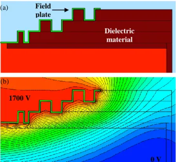
A Field plate termination was used for this structure in order to obtain a maximum breakdown voltage. The optimized field plate length and thickness are 10 um and 0.7 um respectively. The used dielectric in this optimization is the silicon oxide SiO2 [20]. With these parameters, a breakdown
voltage equals 1638 V was obtained. However the maximum electric field located at the end of field plate is 19.5 MV/cm at 700 K.
All results shown in this paper were extracted at 700 K due
to convergence problems at lower temperatures. Other simulations have been performed to evaluate the variation of the electric field peak with temperature. The results show a negligible difference.
III. NEW FIELD PLATE ARCHITECTURE
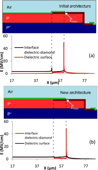
A new idea was proposed in order to increase the breakdown voltage. It is to keep the whole electrode flat, with no corners, and replace the diamond below the field plate region with an optimized thickness of a dielectric material (Fig. 3). Indeed, the presence of corners in the path of the potential strengthens the electric field. In the first architecture, the dielectric is located on the diamond surface, creating a corner in the electrode. At this corner the electric field is stronger in the diamond and then, for the same external voltage, the impact ionization of the first structure is greater than the second one. Consequently, the breakdown voltage of the new structure is higher than the previously proposed one (Fig. 1).
The chosen position, length for the field plate and thickness of the dielectric were respectively 51 µm, 10 µm and 1 µm. With these parameters, the obtained breakdown voltage was equal to 2141 V.
Fig. 3: New field plate architecture for diamond Schottky diode.
The new field plate's architecture required a Reactive Ion Etching (RIE) of diamond with an appropriate thickness, followed by the dielectric deposition (Fig. 4), aluminum wet etch, and finally, the metal deposition for the Schottky contact. Although the dielectric deposition was mastered, it was possible that the thickness of the dielectric is less (Fig. 5 a) or higher (Fig. 5 b) than the one specified.
Fig. 4: Technological process steps to realize the dielectric deposit below the field plate
Electrical simulations were performed in order to study the variation of the field plate efficiency in terms of possible error
1500 2000 2500 3000 3500 4000 4500 5000
0,0E+00 4,0E+15 8,0E+15 1,2E+16 1,6E+16
B re akdo w n vo lta ge (V ) Doping concentration (cm-3) W = 16 µm W = 15 µm W = 14 µm W = 13 µm W = 12 µm W = 11 µm W = 10 µm W = 9 µm W = 8 µm W = 7 µm W = 6 µm W = 5 µm
0 20 40 60 17 37 57 77 E (M V/ cm ) X (µm) Interface dielectric-diamond Dielectric surface
(b)
of the dielectric thickness. Fig. 6 shows this variation. The efficiency decreases by 4% when the error of the dielectric thickness increases from 0 to 0.2 µm. This decrease can be explained by the strengthening of the field plate peak in the semiconductor. Despite this decrease, the efficiency of this field plate topology remains greater than the efficiency of the conventional structure.
Fig. 5: Expected technological difficulties during manufacture of the diodes (a) Dielectric thickness less than desired (Wd<0), (b) Dielectric thickness
higher than expected (Wd> 0).
Fig. 6: Variation of the efficiency of the field plate according to Wd (Fig. 5), Positive values correspond to an excess thickness of dielectric and negative
values to a withdrawal of the dielectric
Fig. 7 shows the electric field distributions for both architectures. Its variation was plotted along the horizontal axis passing along the surface of the dielectric and another passing through the dielectric-diamond interface. In the graph at the top (old architecture, Fig. 7(a)), there are two peaks. The first one is located in the diamond at the beginning of the field plate and the second is at its extremity. The electric field focalization in the diamond in the initial architecture increases the impact ionization and as a result, the breakdown voltage decreases. The graph at the bottom (Fig. 7(b)) shows one peak of the electric field at the extremity of the field plate.
Using a very refine mesh in the maximum electric filed zone (distance between two points equals 10 nm), an electric field equal to 49 MV/cm and 48.5 MV/cm was reported for the initial and new architecture respectively. This electric field peak is situated at the edge of the field plate. Those values are much higher than the maximum electric field stand by high quality of dielectrics, like silicon oxide (10 MV/cm) and silicon nitride (between 5 and 7 MV/cm). In this case, the dielectric breaks for a voltage much lower than the ideal
breakdown voltage and therefore, the field plate does not play its role.
Fig. 7: Electric field distribution at 1700 V (a) in the initial architecture and (b) the new one.
IV. ELECTRIC FIELD OPTIMIZATION
Looking at the experimental results, the average breakdown voltage was 400 V (Fig. 8) [20]. One of the responsible reasons for this failure may be the break of the dielectric. The material impurity can be also another reason for this small break down voltage. Indeed, the material impurities become traps (charge donor or charge receiver), which change the repartition of the equipotential lines and therefore a possible premature breakdown. This paper has focalized for the first reason.
To improve the efficiency of the termination, the dielectric can be changed as Ikeda [8]. He has used Al2O3 as a dielectric
under the field plate, unfortunately, it won't be enough although the high permittivity of the aluminum oxide (Ɛ ≈ 9). Therefore, the goal now is to change the field plate structure in order to minimize the electric field at its edge.
As previously shown in this paper, the maximum electric field is located at the corner. Thus, increasing the number of corners along the potential's lines distribution reduces the
90 91 92 93 94 95 -0,2 -0,1 0 0,1 0,2 Ef fi ci e nc y (% ) Wd (µm) 0 20 40 60 17 37 57 77 E (M V/ cm ) X (µm) Interface dielectric-diamond
Dielectric surface
(a)
(a)
(b)
Wd <0 Wd >0
Emax
electric field value near the edge of the field plate (distribution of peaks). Three architectures may be able to solve this problem.
a- The pillars dielectric form. That means, making the oxide in pillars form until the end of the electrode, which increases the number of corners along the path of the potential as shown in Fig. 9 (a).
b- The graduated dielectric form Fig. 9 (b). c- Mixed dielectric form Fig. 9 (c).
Fig. 8: Experimental electrical characteristics for several reverse-biased diamond Schottky diodes[20].
Fig. 9: Cross section of 3 innovative junction termination structures: (a) pillars oxide form, (b) graduated oxide form, (c) mixed dielectric form.
A. Pillars dielectric form
Using this form, the termination efficiency depends on many parameters: the pillar height, the pillar width, the number of pillars and finally the contact length of the last pillar as shown in Fig. 10. Using this dielectric form, we kept constant the field plate length. The last oxide pillar attains a contact length of 1 micron (CL) (Fig. 10). The pillars width and the distance between pillars equal 2 µm.
Fig. 10: Pillars oxide form.
Fig. 11: Maximum electric field at 1700 V according to pillar height for the pillars field plate form.
Fig. 12: Electric field values at the oxide-oxide interface and the oxide surface for pillars height equal to 1.6 µm at 1700 V and using silicon oxide as a
dielectric. 20 25 30 35 40 45 50 55 60 0 0,4 0,8 1,2 1,6 2 M axi m um e le ct ri c fi e ld (M V /cm ) Pillars height (µm) SiO2 Al2O3 0 5 10 15 20 25 30 35 40 50,5 55,5 60,5 65,5 E (M V /cm ) X (µm) Interface oxide-oxide Oxide surface
Fig. 11 shows the variation of the maximum electric field as a function of the pillars height using two dielectric materials (silicon oxide and aluminum oxide). Increasing the pillars height from 0 to 1.6 µm slightly decreases the breakdown voltage of 25 V, and also the maximum electric field decreases from 37 MV/cm down to 30 MV/cm at 1700 V and down to 30 MV/cm using aluminum oxide as a dielectric material. The field plate overlap on the last pillar plays its role also. Passing from 1 µm as in the previous case to a value of 0.3 µm, the maximum electric field decreases from 37 MV/cm down to 27 MV/cm using silicon oxide as a dielectric. This choice remains very difficult due to photolithography precision. Fig. 12 shows at 1700 V, the electric field variation at the oxide-oxide interface (bb' axis, Fig. 10) and the oxide-oxide surface (aa' axis Fig. 10) for pillars height equal to 1.6 µm. The electric field peaks are located at the corners as the figure shows.
B. Graduated dielectric form
The second proposed field plate structure is the graduated form, where the equipotential lines met three corners before exiting from the device (Fig. 13). Three geometrical parameters play a role in optimizing the architecture: the step oxide height, the number of steps and the field plate overlap on the last step. Only three steps were assumed for the sake of technology process. This oxide form has been previously used by Brezeanu [13] to increase the breakdown voltage and not to minimize the electric field peak in the dielectric. Another work was patented in 1983 [21] use this form in order to reduce curvature of electric field within the body of the semiconductor device underlying the electrode.
Fig. 14 (a) illustrates the electric field distribution in the structure at the protection oxide zone (field plate). Fig. 13 (b) shows a cross sectional view of the electric field for each graduation and at the oxide surface. The electric field peaks at each corner can be seen in this figure. The observed values are larger than those obtained for termination structure with pillars form.
Fig. 13: (a) Graduated oxide form, (b) distribution of electrostatic equipotential lines in the structure termination.
Fig. 15 shows the maximum electric field as a function of the step height using two dielectric materials (silicon oxide and aluminum oxide). The decrease of the breakdown voltage was greater than that of the first architecture (pillars oxide
form) since the total thickness of the oxide was greater. The breakdown voltage therefore decreased from 2141 down to 2080 V (60 V of decreases). At 1700 V the maximum electric field decreased from 53 MV/cm to 33 MV/cm using silicon oxide and from 45 MV/cm to 27 MV/cm using aluminum oxide as a dielectric material. Even though this decrease is important, the electric field does not achieve the required value lower than10 MV/cm for silicon oxide and 8 MV/cm for aluminum oxide.
Fig. 14: (a) electric field distribution in the structure (field plate) (b) cross sectional view of the electric field for each graduation and at the oxide
surface.
Fig. 15: Maximum electric field variation as a function of step height and dielectric material.
C. Mixed dielectric form
The third idea was to combine the two previously proposed solutions. This new idea was so-called mixed dielectric form as shown in Fig. 16. The aim of this form was to maximize the corners number in the path of the equipotential lines without increasing the number of technological steps.
Simulation shows that the maximum electric field at 1700 V equal to 29 MV/cm using the silicon oxide as a dielectric material and 22.7 MV/cm using the aluminum oxide. Fig. 16 a shows the electric field distribution at 1700 V where the electric field peak appear in each corner, that means as soon as there was a tightening of electrostatic potential lines. Using this form the breakdown voltage retains its initial value 2141 V.
Fig. 17 shows a cross sectional view along the horizontal axis through each graduation of the field plate and the surface of the dielectric. This figure shows that, for each curve there are several electric field peaks, which correspond to the number of corners on the electrostatic potential path.
0 5 10 15 20 25 30 50,6 52,6 54,6 56,6 58,6 60,6 62,6 E (M V /cm ) X (µm)
(b)
1700 V (a) (a) (b) 0 V 20 25 30 35 40 45 50 55 60 0 0,4 0,8 1,2 1,6 2 M ax e le ct ri c fi e ld (M V /cm )Oxide step height (µm) SiO2 Al2O3
Fig. 16: (a) Mixed dielectric form of field plate of Schottky diode (b) distribution of equipotential lines in the structure termination at 1700V.
Fig. 17: (a) Electric field distribution above the field plate. (b) Cross sectional view of the electric field along horizontal axis passing through each graduation and on the oxide surface with oxide step thickness equals to
1.6 µm
.
V. CONCLUSION
New field plate shapes for diamond Schottky diode were proposed. The breakdown voltage was improved from 1632 V to 2141 V using the same technological parameters.
The maximum electric field in the field plate induces a new problem since it is larger than the critical field of the used dielectric. To solve this problem, three solutions were proposed. The first one is to define the field plate in a pillars form, the second is to change the field plate to graduated form and the last is a mixed oxide form in order to increase the corners numbers. By using the final solution and changing the dielectric material (from silicon oxide to aluminum oxide) a maximum electric field equal to 22.7 MV/cm was obtained.
Despite the achieved decrease of the electric field peak, this lower value is however higher than the dielectric critical field of the used dielectrics, however, more work is underway in order to more optimize the termination structure.
VI. ACKNOWLEDGEMENTS
This study was conducted in the framework of the topic "simulation, design and realization of high voltage and high temperature power devices" of the LIA (International Laboratory) WIDE-Lab (Wide bandgap technologies for Integration of energy efficient Devices), composed by two French laboratories LAAS and Ampere affiliated at CNRS, and IBM/CNM CSIC laboratory. This work was supported by French FUI project DIAMONIX2
VII. REFERENCES
[1] J.E. Butler, M.W. Geis, K.E. Krohn, J. Lawless, S. Deneault, T.M. Lyszczarz, D. Flechtner, R. Wright, Semiconductor Science and Technology 18 (3) (2003) S67–S71. .
[2] B. Dischler and C. Wild, Low-pressure synthetic diamond: manufacturing and applications, vol. 11. Springer Heidelberg, 1998.
[3] A. T. Collins, S. C. Lawson, G. Davies, and H. Kanda, « Indirect energy gap of 13 diamond », Phys. Rev. Lett., vol. 65, no 7, p. 891‑894.
[4] G. S. Gildenblat, S. A. Grot, and A. Badzian, « The electrical properties and device applications of homoepitaxial and polycrystalline diamond films », Proc. IEEE, vol. 79, no 5, p. 647‑668, 1991.
[5] M. Levinshtein, Handbook Series on Semiconductor Parameters. World Scientific.
[6] S. K. Gupta, N. Pradhan, C. Shekhar, and J. Akhtar, « Design, Fabrication, and Characterization of Ni/4H-SiC (0001) Schottky Diodes Array Equipped With Field Plate and Floating Guard Ring Edge Termination Structures », IEEE Trans. Semicond. Manuf., vol. 25, no 4, p. 664‑672, 2012.
[7] K. Ueno, T. Urushidani, K. Hashimoto, and Y. Seki, « The guard-ring termination for the high-voltage SiC Schottky barrier diodes », IEEE Electron Device Lett., vol. 16, no 7, p. 331‑332, 1995.
[8] K. Ikeda, H. Umezawa, N. Tatsumi, K. Ramanujam, and S. Shikata, « Fabrication of a field plate structure for diamond Schottky barrier diodes », Diam. Relat. Mater., vol. 18, no 2‑3, p. 292‑295, févr. 2009.
[9] M. C. Tarplee, V. P. Madangarli, Q. Zhang, and T. S. Sudarshan, « Design rules for field plate edge termination in SiC Schottky diodes », IEEE Trans. Electron Devices, vol. 48, no 12, p. 2659‑2664, 2001.
[10] M. Bhatnagar, H. Nakanishi, S. Bothra, P. K. McLarty, and B. J. Baliga, « Edge terminations for SiC high voltage Schottky rectifiers », in , Proceedings of the 5th International Symposium on Power Semiconductor Devices and ICs, 1993. ISPSD ’93, 1993, p. 89‑94.
[11] D. Alok and B. J. Baliga, « SiC device edge termination using finite area argon implantation », IEEE Trans. Electron Devices, vol. 44, no 6, p. 1013‑1017, 1997.
[12] K. Ikeda, H. Umezawa, and S. Shikata, « Edge termination techniques for p-type diamond Schottky barrier diodes », Diam. Relat. Mater., vol. 17, no 4‑5, p. 809‑812, april. 2008.
[13] M. Brezeanu, M. Avram, S. J. Rashid, G. A. J. Amaratunga, T. Butler, N. L. Rupesinghe, F. Udrea, A. Tajani, M. Dixon, D. J. Twitchen, A. Garraway, D. Chamund, P. Taylor, and G.
0 5 10 15 20 25 30 50 55 60 65 70 75 80 E (M V /cm ) X (µm) First graduation Second graduation Third graduation Oxide surface
(b)
(a) Field plate Dielectric material 1700 V Field plate (a) 0 V (b)Brezeanu, « Termination Structures for Diamond Schottky Barrier Diodes », in IEEE International Symposium on Power Semiconductor Devices and IC’s, 2006. ISPSD 2006, 2006, p. 1 ‑4.
[14] H. Umezawa, M. Nagase, Y. Kato, and S. Shikata, « Diamond Vertical Schottky Barrier Diode with Al<sub>2</sub>O<sub>3</sub> Field Plate », Mater. Sci. Forum, vol. 717‑720, p. 1319‑1321, may 2012.
[15] G. Brezeanu, M. Brezeanu, C. Boianceanu, F. Udrea, G. A. J. Amaratunga, and P. Godignon, « Impact of High-k Dielectrics on Breakdown Performances of SiC and Diamond Schottky Diodes », Mater. Sci. Forum, vol. 600‑603, p. 983‑986, 2009. [16] « Sentaurus user guide A-2008.09 ». .
[17] A. G. Chynoweth, « Ionization Rates for Electrons and Holes in Silicon », Phys. Rev., vol. 109, no 5, p. 1537‑1540, march 1958.
[18] R. Van Overstraeten and H. De Man, « Measurement of the ionization rates in diffused silicon p-n junctions », Solid-State Electron., vol. 13, no 5, p. 583‑608, may 1970.
[19] S. J. Rashid, A. Tajani, L. Coulbeck, M. Brezeanu, A. Garraway, T. Butler, N. L. Rupesinghe, D. J. Twitchen, G. A. J. Amaratunga, F. Udrea, P. Taylor, M. Dixon, and J. Isberg, « Modelling of single-crystal diamond Schottky diodes for high-voltage applications », Diam. Relat. Mater., vol. 15, no
2‑3, p. 317‑323, feb. 2006.
[20] F. Thion, « Conception de protections périphériques applicables aux diodes Schottky réalisées sur diamant monocristallin », Ph.D. Thesis, INSA de Lyon, 2012.
[21] T. Herman and A. Lidow, « Composite metal and polysilicon field plate structure for high voltage semiconductor devices », Patent, US 4399449 A, 1983.