HAL Id: tel-02064267
https://tel.archives-ouvertes.fr/tel-02064267
Submitted on 11 Mar 2019HAL is a multi-disciplinary open access archive for the deposit and dissemination of sci-entific research documents, whether they are pub-lished or not. The documents may come from teaching and research institutions in France or abroad, or from public or private research centers.
L’archive ouverte pluridisciplinaire HAL, est destinée au dépôt et à la diffusion de documents scientifiques de niveau recherche, publiés ou non, émanant des établissements d’enseignement et de recherche français ou étrangers, des laboratoires publics ou privés.
The atomic struture of inversion domains and grain
boundaries in wurtzite semonconductors : an
investigation by atomistic modelling and high resolution
transmission electron microscopy
Siqian Li
To cite this version:
Siqian Li. The atomic struture of inversion domains and grain boundaries in wurtzite semonconduc-tors : an investigation by atomistic modelling and high resolution transmission electron microscopy. Other [cond-mat.other]. Normandie Université, 2018. English. �NNT : 2018NORMC252�. �tel-02064267�
THÈSE
Pour obtenir le diplôme de doctorat
Spécialité PHYSIQUE
Préparée au sein de l'Université de Caen Normandie
Τhe atοmic struture οf inversiοn dοmains and grain bοundaries in
wurtzite semοncοnductοrs : an investigatiοn by atοmistic
mοdelling and high resοlutiοn transmissiοn electrοn micrοscοpy
Présentée et soutenue par
Siqian LI
Thèse soutenue publiquement le 04/12/2018 devant le jury composé de
M. JOEL DOUIN Directeur de recherche, CEMES Rapporteur du jury
M. ABDELKRIM REDJAIMIA Professeur des universités, UNIVERSITÉ LORRAINE Rapporteur du jury M. JUN CHEN Professeur des universités, UNIVERSITE CAEN NORMANDIE Membre du jury Mme LUCIA REINING Directeur de recherche, ECOLE POLYTECHNIQUE Président du jury M. PIERRE RUTERANA Directeur de recherche au CNRS, 14 ENSI de Caen Directeur de thèse Mme MAGALI MORALES Maître de conférences HDR, UNIVERSITE CAEN NORMANDIE Co-directeur de thèse
Thèse dirigée par PIERRE RUTERANA et MAGALI MORALES, Centre de recherche sur les ions, les matériaux et la photonique (Caen)
Acknowledgments
This thesis has been carried out at CIMAP Laboratory (Centre de recherche sur les Ions, les Matériaux et la Photonique), it was supported by the china scholarship council (CSC) for financial support under the file number 201508420147. My greatest thanks belong to my supervisors Drs.
Pierre Ruterana and Magali Morales for the countless fruitful discussions, suggestions and supports
during this research.
I would like to thank the members of jury: especially M. Joel Douin and M. Abdelkrim Redjaimia who accepted to review my work and Mrs. Lucia Reining, as well as M. Jun Chen for their valuable comments and suggestions.
Special thanks are due to my collaborators, Prof. Hadiç Morkoç, Dr. Barkat Ullah and Dr. Vitaliy
Avrutin who grew the ZnO/GaN heterostructures. I would like to thank Prof. Slawomir Kret
(institute of Physics, Polish Academy of Science (IP-PAS), Warsaw Poland) who hosted me for high-resolution analytical transmission electron microscopy training, along with Dr. Lei Huaping (Heifei Institute of Physics Science, Chinese Academy of Science CAS, Hefei) who kindly introduced me to the first-principles methods with Vienna ab initio simulation package. I am very thankful to Prof.
Jun Chen and Dr. Viwanou Hounkpati who supported and discussed with me about the technical
questions on theoretical calculations.
My gratitude goes to all the PM2E group members: Dr. Albert Minj for his kind help and patient explanations; Dr. Hichem Ben Ammar, Nicolas Chery, Farah Bouazzaoui and Marie-Pierre
Chauvat who brought a lot of happy times and support all along these three years.
Besides, I would like to thank all the following people who always offer me help and support me to overcome the difficulties. My Master degree’s advisor: Prof. Zhang Jun who always encourages and inspires me. Prof. Guosheng Shao and Dr. Zhuo Wang who hosted me for a visit and guided me for my further studies.
I am grateful to the PSIME graduate school for support of my visits out of the University of Caen Normandie. And also, I acknowledge the extensive use of the computer resources of CRIANN "Centre Regional Informatique et d’Applications Numériques de Normandie” under project No. 2016009.
Structure atomique des domaines d’inversion et joints de grains
dans les semiconducteurs wurtzites : Modélisation atomistique
et microscopie électronique haute résolution
Les semiconducteurs nitrures d’éléments III (AlN, GaN, InN) et le ZnO de structure wurtzite sont des matériaux d'une grande importance pour les applications optoélectroniques en raison de leurs larges bandes directes qui couvrent la plus large gamme de longueurs d’onde d’émission pour une seule famille de matériaux de l’ultraviolet lointain (6.2 eV) au proche infrarouge (0.65 eV) en ce qui concerne les nitrures. Ils sont donc très attendus pour de très nombreuses applications en optoélectronique et microélectronique. Ils sont le sujet de recherches très intenses pour optimiser la qualité des couches minces, et donc les investigations portent sur tous les aspects : les mécanismes de croissance, les propriétés structurales comme l'élasticité, la polarité, les défauts cristallins, etc. ... En effet, dans ces couches minces obtenues par épitaxie sur divers substrats, les défauts de croissance vont jouer un rôle important sur les propriétés du matériau et les performances de dispositifs. Au cours de ce travail, nous avons étudié particulièrement deux types de défauts plans: l’inversion de polarité dans le plan (0001), et les joints de grain de rotation autour de l’axe [0001]. Nous avons ainsi pu déterminer la structure atomique la plus stable dans ce plan d’inversion pour les composés wurtzite et l’hétérostructure ZnO/GaN et ensuite celle des joints, grâce à deux approches complémentaires menées en parallèles: l’investigation au microscope électronique haute résolution et la modélisation atomistique par des techniques ab initio. Ceci nous a permis non seulement de connaître la structure intime, mais aussi de mettre en évidence les propriétés électroniques correspondantes.
Le manuscrit de cette thèse contient six chapitres:
Le chapitre 1 examine les propriétés structurelles et électroniques fondamentales des composés des nitrures et de ZnO, en passant d’abord en revue la structure wurtzite, ses propriétés élastiques, et la polarité induite. Dans ce chapitre, nous avons aussi décrit brièvement les techniques de croissance des matériaux analysés, ainsi que les principaux défauts rencontrés dans les couches minces correspondantes.
Le chapitre 2 rappelle la théorie de la densité fonctionnelle et introduit les principales approximations qui ont permis d’aborder de façon raisonnable la résolution de l’équation de Schrödinger, jusqu’aux programmes de résolution pratiques que nous avons utilisés dans ce travail.
Dans le chapitre 3, nous présentons les résultats obtenus sur la structure du plan d’inversion (0001) dans ZnO et les nitrures d’éléments III. Il s’agit d’une modélisation entièrement théorique où nous avons analysé la stabilité structurale, les propriétés de liaison chimique ainsi que la structure électronique.
Le chapitre 4 propose une corrélation entre les analyses de la structure atomique par microscopie haute résolution et la modélisation ab initio de l’inversion de polarité à l’hétérointerface ZnO/GaN. Ainsi, la configuration la plus stable du point de vue énergétique a été déterminée, et imposée par la polarité Ga du substrat GaN, il est montré que cette inversion dans une monocouche se forme sur une couche métallique contrairement à ce qui avait été rapporté auparavant.
Dans le chapitre 5, nous discutons des résultats originaux obtenus sur des joints de grains de rotation autour de l’axe [0001] qui est la direction de croissance des couches étudiées. Plus particulièrement en utilisant le dépôt en phase vapeur assisté par plasma, nous avons pu obtenir des couches de ZnO polycristallin sur saphir avec seulement deux orientations: en maintenant l’axe [0001] commun, les nano-domaines adjacents avaient leurs axes [112�0] et [101�0] parallèles. Théoriquement, il y avait donc une rotation de 30° ou alors de 90° entre ces domaines. Par microscopie haute résolution, nous avons systématiquement observé la formation des joints de grain de type Ʃ13, de rotation de 32.2° ou 27.8°. Plus intéressant, les interfaces correspondantes étaient systématiquement soit le côté ou alors la diagonale de la cellule unitaire de coïncidence. Ainsi, nous avons eu la possibilité de montrer que le concept d’unités structurales existait dans la structure wurtzite. En effet, pour la première fois, et pour quatre joints de grains, on peut observer exactement les dislocations prévues par la théorie topologique. Plus particulièrement dans ZnO, la structure atomique de la dislocation coin [101�0] avec un cœur spécifique large de 486-atomes est montré comme une unité structurale fondamentale pour ces joints de grain de symétrie wurtzite.
Introduction
Group III-nitrides and ZnO semiconductors are of great importance materials for the optoelectronics applications due to their wide direct band gaps which cover from the ultraviolet to infrared energy range. It has been a subject of intense investigations on their structural properties like elasticity, polar nature et al., growth mechanism such as polarity control, as well as lattice defects. Among these investigations, the structural defects gained from the film epitaxy growth may influence the material property and further degrade the device performances which consequently received a great deal of attentions in this field. With the thesis, we pay more attention to the two kinds of planar defects: (0001) plane inversion domain boundary (IDB) and [0001] tilt grain boundary (GB). The aim of this work is to clarify the interfacial configuration of (0001) plane IDB at ZnO/GaN heterointerface and the core structure of [0001] tilt GB using precise atomic scale STEM measurements and extensive theoretical simulations. Furthermore, based on the determined atomic structures, the electronic properties are studied as well.
The doctoral dissertation is segmented into five chapters:
Chapter 1 reviews the fundamental structural and electronic properties of group III-nitrides and ZnO compounds including wurtzite crystal, elasticity character, and polarization. In addition, several thin film growth techniques and the selected planar defects are introduced as well.
Chapter 2 briefly reviews the development of density functional theory. Some particular approximations and algorithms are introduced. At the end, the advantages of two kinds of ab initio packages used in this thesis are related.
Chapter 3 deals with the investigation of (0001) plane inversion domain boundary in group III-nitrides and ZnO homogeneous compounds. A completely theoretical calculation is presented. Comparison of structural stability, chemical bonding properties as well as the defective state in electronic structure are analyzed in this chapter.
Depending on the theoretical investigations in chapter 3, the (0001) plane IDBsare implemented in more complex interface, ZnO/GaN heterointerface, since the lattice mismatch between the two materials is moderate (1.8%) and successfully achievement of ZnO/GaN heterojunction based devices. Chapter 4 first presents a serial of atomic scale TEM
images to uncover that polarity reversal took place at one monolayer at ZnO/GaN heterointerface. Based on the theoretical studies in chapter 3, eight (0001) plane IDB models are constructed for the ZnO/GaN heterointerface and their thermodynamical stability, chemical bonding as well as electron structure are investigated.
Chapter 5 discusses a study of [0001] tilt GBs in ZnO. High-resolution TEM is used to analyze the core structure of grain boundaries. For the first time, the [101�0] edge dislocation with a specific core of 486-atom ring is shown to be a characteristic structural unit of this grain boundaries of wurtzite symmetry in agreement with early theoretical reports. Furthermore, the defective state on valence band edge is discussed as well.
T
able of contents
Acknowledgements i
Introduction v
Table of Contents vii
Chapter 1 Wurtzite Semiconductors 1
1.1 Crystal Structure and Related Properties 1
1.1.1 Crystal Structure 1
1.1.2 Elastic Strain 3
1.1.3 Polarity Property 4
1.2 Growth Techniques 8
1.2.1 Substrates 8
1.2.2 Plasma-Induced Molecular Beam Epitaxy (PIMBE) 9
1.2.3 Plasma-Assisted Sputtering 10
1.3 Extended Defects 11
1.3.1 Inversion Domain Boundaries (IDBs) 11
1.3.2 Grain Boundaries (GBs) 14
References 17
Chapter 2 Density Functional Theory and Application Techniques 20
2.1 Schrödinger Equation 20
2.2 Born-Oppenheimer Approximation 21
2.3 Density Functional Theory 22
2.3.1 The Hohenberg-Kohn Theorems 23
2.3.2 The Kohn-Sham Equations 24
2.3.3 Exchange-Correlation Functional 25
2.4 Hybridization Functional Method 28
2.5 On-Site Coulomb Repulsion Correction-DFT+U 29
2.6 Computational Methods 30
2.6.1 Simulation Packages 30
2.6.2 Relative Formation Energies 34
2.6.3 Chemical Bonding Properties 35
2.6.4 Electronic Structures 37
References 39
Chapter 3 (0001) Plane Inversion Domain Boundaries in Wurtzite Semiconductors 42
3.1 Introduction 42
3.2 Simulation Method 43
3.3 Energetic Stability 44
3.4 Chemical Bonding and Bader Population Analysis 45
3.5 Electron Structure of IDBs 50
3.5.1 Band Structure 50
3.5.2 Projected Density of States (PDOS) 52
3.6 Conclusion 54
References 55
Chapter 4 Experimental and Theoretical Investigation of the (0001) Plane IDBs at the ZnO/GaN heterointerface 57
4.1 Introduction 57
4.2 Samples 59
4.3 TEM Observation 61
4.4 Theoretical Modeling of (0001) Plane IDBs in ZnO/GaN heterostructure 64
4.6 Chemical Bonding and Bader Population Analysis 69
4.7 Electronic Structure of IDBs 74
4.8 Conclusion 76
References 77
Chapter 5 [0001] Tilt Grain Boundaries in ZnO Semiconductor 82
5.1 Introduction 82
5.2 Topological Analysis of GBs in Wurtzite Symmetry 84
5.3 Methodology 88
5.3.1 Experimental Procedures 88
5.3.2 Computational Details 89
5.4 The Atomic Structure of the [101�0] Edge Dislocation 91
5.4.1 The [101�0] Edge Dislocation in GaN 92
5.4.2 The [101�0] Edge Dislocation in ZnO 94
5.5 Electronic Properties of GBs 103
5.6 Conclusion 105
References 106
Chapter 6 General Conclusion and Perspective 110
6.1 General Conclusion 110
Chapter 1
Wurtzite Semiconductors
The group III-nitrides and ZnO semiconductors have attracted a great deal of attentions due to their prominent properties such as large direct band gaps (GaN, AlN and ZnO) and high exciton binding energy (~60 meV in ZnO) which have applications in optoelectronic and electronic fields. In this chapter, basic properties encompassing crystallography, elastic constants, polarity, electronic properties, crystal growth, as well as crystal defects are briefly introduced.
1.1 Crystal Structure and Related Properties
1.1.1 Crystal Structure
AlN, GaN, InN and ZnO are the most stable in wurtzite (WZ) structure at ambient conditions. In this structure, the atoms occupy tetrahedral sites with each atom bonded to four neighbors of the other atomic species. The respective topology is shown in Figure 1.1 [1]. The unit cell consists of two interpenetrating hexagonal close packed sublattices, in which one of the sublattices is shifted along the c-axis by a relative displacement of u in fractional coordinates (seen in Figure 1.1(a)). In an ideal WZ crystal, the two lattice constants, a and c, are related by 𝑐𝑐
𝑎𝑎=�8 3⁄ = 1.633 and the internal parameter u equals to 3/8=0.375. The side view of Figure 1.1(b) indicates a stacking sequence of -AaBbAaBb- along the [0001] axis.
The dashed lines in side view of Figure 1.1(b) denote the projected positions (A or B sites) along [0001] direction. Due to the different ionicities (ionic radii) of the cations respect to the anions, the group III-nitrides and ZnO exhibit various lattice parameters. Table 1.1 gathers a set of lattice parameters: c/a ratio and u parameter for AlN, GaN, InN and ZnO either from experiments or from theoretical calculations. As can be seen,
the c/a ratios and u parameters slightly vary from the ideal values of 1.633 and 0.375, which depends on the atom sizes.
Figure 1.1. Topology of wurtzite crystal including stick-ball model (a) and side view (b)
presentations. Solid and hollow dots represent the cation and anion. Atomic stacking sequence is shown aside [1].
Table 1.1 Lattice parameters a, c (Å), internal parameter u, as well as c/a ratio of WZ structure
for the group III-nitrides and ZnO semiconductors.
a (Å) c (Å) u c/a AlN 3.112a 4.983a 0.380b 1.601 GaN 3.189a 5.185a 0.376b 1.626 InN 3.545a 5.703a 0.377b 1.609 ZnO 3.250c 5.204c 0.382c 1.602 aFrom [2] bFrom [3] cFrom [4]
1.1.2 Elastic Strain
The elasticity of the solid allows the material to deform under the external force induced by impurities, lattice mismatch etc., and completely recovers its initial state with removal of the stress. The lattice deformation induced by the stress is called strain. The relationship between the stress σ and the strain ε is defined by the generalized Hook’s law [5]:
σ𝑖𝑖𝑖𝑖 =𝐶𝐶𝑖𝑖𝑖𝑖𝑖𝑖𝑖𝑖𝜀𝜀𝑖𝑖𝑖𝑖 (1.1) where 𝐶𝐶𝑖𝑖𝑖𝑖𝑖𝑖𝑖𝑖 is the elastic stiffness coefficient related to stress tensor 𝜎𝜎𝑖𝑖𝑖𝑖 and strain tensor 𝜀𝜀𝑖𝑖𝑖𝑖. With hexagonal symmetry, five independent elastic stiffness constants: 𝐶𝐶11, 𝐶𝐶12, 𝐶𝐶13 , 𝐶𝐶33 and 𝐶𝐶44 are included to simplify the matrix as:
(1.2) where the Voigt notation is employed: 𝑥𝑥𝑥𝑥 → 1, 𝑦𝑦𝑦𝑦 → 2, 𝑧𝑧𝑧𝑧 → 3, 𝑦𝑦𝑧𝑧, 𝑧𝑧𝑦𝑦 → 4, 𝑥𝑥𝑧𝑧, 𝑧𝑧𝑥𝑥 → 5, 𝑥𝑥𝑦𝑦, 𝑦𝑦𝑥𝑥 → 6. In the matrix, x, y, z-axes are parallel to the orthogonal crystal axis [21�1�0], [011�0] and [0001], respectively And 𝐶𝐶66 equals to (𝐶𝐶11− 𝐶𝐶12)/2. In most cases including wurtzite single crystal, the elastic constants are evaluated by measuring the velocity of sound after applying the transverse and longitudinal waves along the c axis and any axis perpendicular to it [5], table 1.2 reports elastic constants taken from the literature.
Table 1.2 Elastic constants of the group III-nitrides and ZnO compounds (GPa).
1.1.3 Polarity
The wurtzite structure (space group: P63mc) does not have a center of symmetry along
the [0001] direction (Fig. 1.2). So that a crystal film grown along this direction is polar. By convention, the positive polarity [0001] has been defined as when the c axis is pointing from the cation to the anion.
Figure 1.2. The polarity lay out in wurtzite, the case of GaN [1].
The polarity of group III-nitrides and ZnO has a marked influence on material growth and electronic properties. For instance, as reported in experiments, the growth of GaN
WZ C11 C12 C13 C33 C44 AlNa 396 137 108 373 116 GaNb 390 145 106 398 105 InNa 223 115 92 224 48 ZnOc 209.7 121.1 105.1 210.9 42.5 aFrom [6] bFrom [7] cFrom [8]
rough on top of the N-face [9]. The results are similar with the growth of ZnO films [10]. As for the influence on electronic properties, the most typical application refers to high electron mobility transistors (HEMTs) in which a two-dimensional electron gas (2DEG) can be obtained at heterointerfaces without the need of doping like in cubic semiconductors [11]. Without considering external fields, the macroscopic polarization is given as a sum of spontaneous polarization 𝑃𝑃𝑆𝑆𝑆𝑆 in equilibrium condition and strain generated piezoelectric polarization 𝑃𝑃𝑆𝑆𝑃𝑃 as:
P = P𝑆𝑆𝑆𝑆+ P𝑆𝑆𝑃𝑃 (1.3) In the following section, the determination and derivation of spontaneous and piezoelectric polarization are briefly introduced.
Spontaneous Polarization
Spontaneous polarization of group III-nitrides and ZnO wurtzite semiconductors directly results from the absence of inversion symmetry along the c axis. Figure 1.3 shows the diagram of dipole moments in wurtzite GaN. Due to the difference of electronegativities between Ga and N atoms, Ga-N bond is polarized with a dipole moment of 𝑃𝑃0 pointing from N to Ga. The asymmetry along the c axis leads to a permanent dipole moment along the [0001] direction, named as spontaneous polarization 𝑃𝑃𝑆𝑆𝑆𝑆. The absolute value of spontaneous polarization is unknown and can only be calculated as a relative value with respect to an “unstrained” material reference like zinc-blend structure. Table 1.3 lists the values of spontaneous polarization from Ref.[12]. It is worth noting that the reference structure must have ideal values of c/a=1.633 and u=0.375. As the real lattice parameters can be distorted through small deviations, the obtained polarization values are sensitive to the lattice parameters used in the calculations.
Figure 1.3. Ball-and-stick diagram of the tetrahedral bonding in wurtzite GaN for Ga- (a) and
N-polarity (b) configuration, respectively. The dipole moments of polarized Ga-N bond are shown.
Piezoelectric Polarization
Apart from the spontaneous polarization, the strain induced or piezoelectric polarization PPE has also important influence on electronic properties of the group
III-nitrides and ZnO compounds. Similar with the elastic stress, in the linear regime, the piezoelectric polarization is approximatively given as a linear function of elastic strain by:
P𝑖𝑖𝑆𝑆𝑃𝑃 =𝑒𝑒𝑖𝑖𝑖𝑖𝑖𝑖𝜀𝜀𝑖𝑖𝑖𝑖 (1.4) In hexagonal symmetry, the three non-vanishing and independent piezoelectric constants are: 𝑒𝑒33, 𝑒𝑒13, 𝑒𝑒15. The piezoelectric polarization components along the three axes can be deduced as:
P1𝑆𝑆𝑃𝑃 =𝑒𝑒15𝜀𝜀5 (1.5) P2𝑆𝑆𝑃𝑃 =𝑒𝑒15𝜀𝜀4 (1.6) P3𝑆𝑆𝑃𝑃 =𝑒𝑒31(𝜀𝜀1+𝜀𝜀2) +𝑒𝑒33𝜀𝜀3 (1.7) The coefficient 𝜀𝜀3 denotes the strain along the c-axis and is expressed as 𝜀𝜀3 = (𝑐𝑐 − 𝑐𝑐0)/𝑐𝑐0. As the in-plane strain in (0001) plane is biaxial, 𝜀𝜀1 =𝜀𝜀2 = (𝑎𝑎 − 𝑎𝑎0)/𝑎𝑎0, 𝑐𝑐0 and 𝑎𝑎0are the equilibrium lattice constants of WZ structure. Based on Berry phase approach
[13], Bernardini and Fiorentini [12] calculated the polarization constants for all group III-nitrides and compared the results with the conventional III-V and II-VI compounds. Table 1.3 collects the calculated spontaneous polarization and the piezoelectric constants for our compounds using the set of lattice parameters from Ref. 12. The spontaneous polarization has negative sign and increases from GaN over InN to AlN. In particular, the piezoelectric response of AlN is comparable to that of ZnO which is reported to possess the highest piezoelectric polarization among the tetrahedrally bonded compounds.
In case of biaxial strain, the lattice parameters a and c in hexagonal symmetry have the relationship: 𝑐𝑐−𝑐𝑐0 𝑐𝑐0 = −2 𝐶𝐶13 𝐶𝐶33 𝑎𝑎−𝑎𝑎0 𝑎𝑎0 (1.8)
The piezoelectric polarization along c axis in Eq.(1.7) is then determined by:
𝑃𝑃3𝑆𝑆𝑃𝑃 = 2𝑎𝑎−𝑎𝑎𝑎𝑎00(𝑒𝑒31− 𝑒𝑒33𝐶𝐶𝐶𝐶1333) (1.9)
From the piezoelectric constants tabulated in Table 1.3, �𝑒𝑒31− 𝑒𝑒33𝐶𝐶𝐶𝐶1333� < 0, therefore, the piezoelectric polarization is negative for tensile strain and positive for compressive strain, respectively.
The polarization induced interfacial sheet charge density is given as the change of polarization between the lower and the upper layer:
𝜎𝜎 = 𝑃𝑃𝐿𝐿𝐿𝐿𝐿𝐿𝐿𝐿𝐿𝐿− 𝑃𝑃𝑈𝑈𝑈𝑈𝑈𝑈𝐿𝐿𝐿𝐿 = (𝑃𝑃𝐿𝐿𝐿𝐿𝐿𝐿𝐿𝐿𝐿𝐿𝑆𝑆𝑆𝑆 +𝑃𝑃𝐿𝐿𝐿𝐿𝐿𝐿𝐿𝐿𝐿𝐿𝑆𝑆𝑃𝑃 )− �𝑃𝑃𝑈𝑈𝑈𝑈𝑈𝑈𝐿𝐿𝐿𝐿𝑆𝑆𝑆𝑆 +𝑃𝑃𝑈𝑈𝑈𝑈𝑈𝑈𝐿𝐿𝐿𝐿𝑆𝑆𝑃𝑃 � (1.10) If the charge density σ is positive , electrons will accumulate at the interface region to form a so-called two-dimensional electron gas (2DEG); but if σ is negative, a
2-dimensional hole gas (2DHG) takes place at the interface.
Table 1.3 Theoretical results of spontaneous polarization and the piezoelectric coefficients for
the group III-nitrides and ZnO. The values are given in (C/m2).
1.2 Growth Techniques
In this section, a few growth methods are reviewed with a particular attention focused on the plasma-induced molecular beam epitaxy (PIMBE) and magnetron sputtering that have been used to grow our samples.
1.2.1 Substrates
The foreign substrates are necessary for obtaining high quality layers in case no bulk material is available at an affordable price. Due mostly to the large availability and symmetry compatibility, as well as moderate thermal expansion mismatch, silicon [14] and silicon carbide (SiC) [15] and sapphire (α-Al2O3) [16] are the most popular
substrates used to grow group III-nitrides and ZnO. Besides, the heteroepitaxy of ZnO on GaN can be used to yield a better performance. The combination of GaN and ZnO is stimulated by the moderate lattice mismatch (~2.1%) between the two materials, but also mainly due to the unavailability of stable and reproducible p-type doping of ZnO. With the growth of p-GaN/n-ZnO heterojunction applications for light emission may
Ref.[12] PSP e33 e31
AlN -0.081 1.46 -0.60 GaN -0.029 0.73 -0.49 InN -0.032 0.97 -0.57 ZnO -0.057 0.89 -0.51
be foreseen [17].
1.2.2 Plasma-Induced Molecular Beam Epitaxy (PIMBE)
MBE is one of the main methods to grow thin films of semiconductors, insulators as well as metals [18]. It offers precise control of growth rate within one monolayer which is interesting for achieving sharp interface for an accurate tuning of the properties. Different from the metalorganic chemical vapour deposition (MOCVD) which operates under the thermodynamical equilibrium and mostly relies on diffusion process, MBE uses impinging beams reaction on the substrate surface [19].
Figure 1.4 shows a diagram of MBE chamber. For group III-nitrides or ZnO film growth, as reported by Moustakas et al. [20], an electron cyclotron resonance (ECR) may be mounted in the metal effusion cell port to evaporate the atoms; Nitrogen flux is provided via a compact plasma source or second ECR. Through the process, the strong triple bond between two nitrogen atoms in N2 is dissociated [21-23] to produce the
chemically reactive nitrogen radicals under reduced pressure. Thus, the group III-nitrides and ZnO grow by the synergetic effects of the evaporation of metal resource from the effusion cell and the plasma produced nonmetal radical flux.
The MBE growth process follows the three steps: 1) surface cleaning. In the used ultrahigh vacuum, the substrate is first exposed to a nitrogen plasma in order to remove the residual impurities. Taking the ZnO/GaN as an example, GaN substrate surface is pre-exposed to a Zn flux to saturate or remove the Ga top atomic layer. 2) Lower temperature nucleation growth. In this case a ZnO nucleation layer of 25 nm thickness is deposited at 300°C. 3) Finally, a high temperature up to 670°C is adopted to perform an epitaxial growth of ZnO. During the film growth stage, by varying the ratio of metal or nonmetal flux, the speed of step flow growth, surface’s morphology, as well as the polarity can be well controlled.
Figure 1.4. Schematics of a molecular beam epitaxy chamber. A Plasma or ECR source is used
to generate chemically active nitrogen atoms [24].
1.2.3 Plasma-Assisted Sputtering
Modern Plasma assisted sputtering is based on a plasma which is generated between a target and the substrate at low pressure using a closed magnetic field at 13.56 MHz. In this process, a pre-sputtering process is needed in order to remove the contamination on the target material surface. A mixture of nitrogen and argon is utilized to serve as the N-resource and sputtering gas. Figure 1.5 schematically exhibits the work principle of magnetron sputtering. The positively charged ions from the plasma are accelerated by an electrical field superimposed on the negatively charged electrode or “target” with a potential range from few hundred to few thousand electron volts, and strike the negative electrode until the atoms are ejected from the target material. Those dislodged metal atoms will condense on the top of the substrate which is in proximity to the sputtering cathode. The substrate holder is rotatable and we could place the substrate above either sputtering source to allow for the sequential deposition required for bilayer and multilayer films. The obtained films by sputtering are in general polycrystalline or columnar, we shall investigate the atomic structure of their boundaries in chapter 5.
Figure 1.5. Diagram of magnetron sputtering system: the source is a target made of the
material to be deposited [24].
1.3 Extended Defects
The materials under study are grown on foreign substrates such as Al2O3 and SiC which
generates a high density of structural defects (up to 1010 cm-2) [25,26] due to the
mismatch of lattice parameters and expansion coefficients. There is a great need for investigating the crystal defects since they can degrade the electronic and mechanical properties of the material, with a highly detrimental effect on device performance. This work focuses on two kinds of planar defects: the (0001) plane inversion domain boundary (IDB) and the [0001] tilt GBs in ZnO through investigation within a close combination of high-resolution TEM observations and theoretical modelling.
1.3.1 Inversion Domain Boundaries (IDBs)
The reports on the polarity control of wurtzite layers along the c axis displays a number of controversial conclusions. For example, Xia et al. [27] have reported that low growth temperature (<500°C) and Ga-rich condition lead to a Ga-polar GaN based on O face ZnO; whereas, N-polar GaN can be achieved on O face ZnO by using high growth temperature and low III/V ratio. However, Ohgaki et al. [28] have pointed out that the polarity inverted GaN epilayer based on O face ZnO mainly comes from the very thin interfacial layer of Ga2O3.
The IDB is a planar interface between two parts of a crystalline material which are connected by a polarity reversal. It was first reported by Aminoff and Broom in wurtzite ZnO [29], however other terms have also been used to name the same defect such as inversion twins [30], antistructure or antiphase boundaries (APB) [31,32]. Up to now extensive atomic structure and properties investigations have been carried out on the {101�0} prismatic IDBs. Four models of {101�0} IDBs have been reported in the literature. Austerman et al. have proposed two models [30] obtained by keeping the anion (cation) sublattice continuous when crossing the boundary, whereas the cation (anion) sublattice switch to an equivalent tetrahedral site for the polarity reversal. The Holt IDB model [33], as shown in Figure 1.6 (a), is a pure inversion operation across the boundary, it exhibits wrong bonds inside the boundary plane. This kind of structure has been reported to be energetically unfavorable [34], it may change to a more stable configuration through a translation of 1/2[0001], as shown in Figure 1.6(b).
Figure 1.6. [112�0] projections of (a) Holt IDB and (b) IDB* models. Large (cation) and small (anion) circles represent the different elements. The wurtzite stacking sequence of -ABAB- is shown on the left side [33].
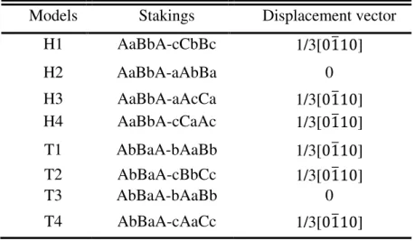
For the (0001) IDB, Kim and Goo [35] have reported a TEM observation on the “pure” (0001) plane IDB structure and proposed eight geometrical models. Their projections along the [112�0] direction are exhibited in Figure 1.7 using their notation, where H stands for head to head and T for tail to tail. As can be seen, H1 and H4 IDBs exhibit similar structural features: a metal atomic layer locates at octahedral position sharing six nearest neighbor nonmetallic atoms at the interface, which in turn bond to the adjacent layer of tetrahedrally coordinated metal atoms. The difference between H1 and H4 IDB comes from the adjacent atomic bi-layer which shifting from Bb location in H1 to Aa in H4. In H2 and H3 IDBs, an aligned metal-nonmetal-metal atomic arrangement is shown: the nonmetal atomic layer at interface bonds to two metal layers with an angle of 180° in deviation of tetrahedral occupation. As for the T IDBs, the interface is made of a nonmetallic atomic layer where each atom is surrounded by six nearest metal atoms occupying tetrahedral sites. The corresponding displacement vectors are given in Table 1.4.
Figure 1.7. Atomic structures of the eight (0001) plane IDBs projected along the [112�0] direction. The green and blue balls represent metal and nonmetal atoms, respectively. The arrows indicate the polarity.
Table 1.4 The stacking sequences and displacement vectors of models in Figure 1.7.
1.3.2 Grain Boundaries (GBs)
A GB is a more complex interface which connects two adjacent crystals of the same material, where the acting symmetry element may be a combination of more than one operation. It always involves a rotation which does not belong to the symmetry group of the crystal. When it results from a pure rotation (Figure 1.8), it can be represented by 𝜃𝜃°[ℎ𝐿𝐿�⃗,𝑘𝑘𝐿𝐿�⃗,𝑙𝑙𝐿𝐿�⃗], (ℎ𝑛𝑛�⃗𝐴𝐴,𝑘𝑘𝑛𝑛�⃗𝐴𝐴,𝑙𝑙𝑛𝑛�⃗𝐴𝐴), the rotation thus takes place around a common axis 𝑜𝑜⃗ = [ℎ𝐿𝐿�⃗,𝑘𝑘𝐿𝐿�⃗,𝑙𝑙𝐿𝐿�⃗] and θ° is the rotation angle. It is simpler to refer to the boundary plane using the coordinates of one of the grains (ℎ𝑛𝑛�⃗𝐴𝐴,𝑘𝑘𝑛𝑛�⃗𝐴𝐴,𝑙𝑙𝑛𝑛�⃗𝐴𝐴).
Depending on the angle between the rotation axis 𝑜𝑜⃗ and the boundary plane normal vector 𝑛𝑛�⃗, grain boundaries are tilt GBs (𝑜𝑜⃗ ⊥ 𝑛𝑛�⃗), twist GBs (𝑜𝑜⃗‖𝑛𝑛�⃗), or of mixed grain type [37]. Moreover, they are also termed as low-angle (<15°) and high-angle (>15°) GBs according to the value of rotation angle θ.
Models Stakings Displacement vector H1 AaBbA-cCbBc 1/3[01�10] H2 AaBbA-aAbBa 0 H3 AaBbA-aAcCa 1/3[01�10] H4 AaBbA-cCaAc 1/3[01�10] T1 AbBaA-bAaBb 1/3[01�10] T2 AbBaA-cBbCc 1/3[01�10] T3 AbBaA-bAaBb 0 T4 AbBaA-cAaCc 1/3[01�10]
Figure 1.8. In a pure rotation grain boundary, xA-zA and xB-zB are the basis vectors of grains A
and B. Boundary plane is determined by its normal vector n. The connecting operation between two grains is a rotation of angle θ around the direction o [36].
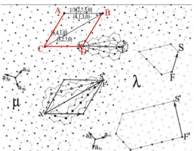
Coincidence-Site Lattice (CSL) Model
The coincidence-site lattice model for the GBs was proposed by Kronberg and Wilson [38] in an attempt to describe the atomic structure of the boundaries. In this formalism, the lattices are artificially interpenetrated and one of them is rotated around the 𝑜𝑜⃗ axis by θ. The results is that for specific angles, sites of the two lattice coincide, which lead to the as-called coincidence-site lattice (CSL). Indeed, it is understandable that the low energy GBs correspond to the highest density coincidence of the two grains and the density of the coincidence site, Σ, was adopted to denominate the grain boundaries as:
Ʃ = 𝑉𝑉𝐿𝐿𝑖𝑖𝑉𝑉𝑉𝑉𝐿𝐿 𝐿𝐿𝑜𝑜 𝑉𝑉𝑛𝑛𝑖𝑖𝑢𝑢𝑐𝑐𝐿𝐿𝑖𝑖𝑖𝑖 𝑖𝑖𝑛𝑛 𝐶𝐶𝑆𝑆𝐿𝐿𝑉𝑉𝐿𝐿𝑖𝑖𝑉𝑉𝑉𝑉𝐿𝐿 𝐿𝐿𝑜𝑜 𝑉𝑉𝑛𝑛𝑖𝑖𝑢𝑢𝑐𝑐𝐿𝐿𝑖𝑖𝑖𝑖 (1.11) Subsequently, the formalism of dichromatic complexes proposed by Pond and Vlachavas [39] is used to determine symmetry operations common to the two grains. In hexagonal symmetry, the rotation angle of θ is identical with (60°-θ) around the tilt axis of [0001]. As can be seen in Figure 1.9, two misoriented grains are designed as black (μ) and white (λ), the coincident sites are clearly visible in the overlap region of two crystals with the periodic unit cell shown by ABDC. Thus, the density of the
coincidence site is given as:
Ʃ =𝑆𝑆𝐴𝐴𝐴𝐴𝐴𝐴𝐴𝐴
𝑆𝑆𝜇𝜇 (1.12)
Using μ as the reference crystal, 𝐴𝐴𝐴𝐴 = −3𝑎𝑎3+𝑎𝑎2 ,𝐴𝐴𝐶𝐶 = 𝑎𝑎3+ 4𝑎𝑎2, thus 𝑆𝑆𝐴𝐴𝐴𝐴𝐴𝐴𝐶𝐶 = 𝐴𝐴𝐴𝐴 × 𝐴𝐴𝐶𝐶 = 13|𝑎𝑎3×𝑎𝑎2|; applying to Eq.(1.12), the Sigma value can be obtained as:
Ʃ = 13|𝑎𝑎3×𝑎𝑎2|
𝑎𝑎3×𝑎𝑎2 = 13 (1.13) Therefore, the grain boundary in Figure 1.9 can also be recognized as Σ13 [0001] tilt GB. The GB is periodic with coincidence sites connected by structural defects [40]. These defects are called the primary dislocations of the grain boundary, they are found through the usual Burgers circuits which enclose one period and travel from μ to λ crystal. When such circuits are mapped into the λ or µ crystal, a unique defect content is obtained which correspond to such a dislocation.
For Σ13 GB in Figure 1.9, for the side of CSL unit cell AB {4�, 1,3,0}, the Burgers circuit is exhibited as SXF (𝐶𝐶𝜇𝜇 = −3𝑎𝑎3+𝑎𝑎2 ,𝐶𝐶𝜆𝜆 =𝑎𝑎3− 3𝑎𝑎2). When mapping this Burgers circuit in λ crystal, an a edge dislocation core with the defect content of -2a1λ
is obtained. Similarly for the diagonal of CSL, unit cell BC {5�, 2,7,0} boundary, the defect content comes out as F'S'=2(a3-a1)λ.
Equipped with the basic topology above, the type and the Burgers vector of the defect content can be directly determined. Their defect core structure can be identified further by high-resolution TEM and atomic modelling.
Figure 1.9. Dichromatic complex of the CSL for Σ13 GB at 32.2°. A superposition of sublattices
μ and λ is shown. The Burgers circuits for the side AB {4�, 1,3,0} and diagonal BC {5�, 2,7,0} boundaries are mapped in crystal λ. The rotation axis is along [0001] direction [40]
References
[1] T. Hanada, Basic Properties of ZnO,GaN, and Related Materials, in: T. Yao and S-K Hong (Eds.), Oxide and Nitride Semiconductors, Springer Verlag, pp.1-18. [2] I. Vurgaftman, J.R. Meyer, J. Appl. Phys. 94, 3675 (2003).
[3] F. Bernardini, V. Fiorentini, D. Vanderbilt, Phys. Rev. B 56, R10024 (1997) [4] H. Karzel, W. Potzel, M. Köfferlein, W. Schiessl, M. Steiner, U. Hiller, G.M.
Kalvius, D.W. Mitchell, T.P. Das, P. Blaha, K. Schwarz and M.P. Pasternak, Physical Review B: Condensed Matter, 53, 11425 (1996).
[5] M. Levy, Introduction to fundamentals of elastic constants, in: M. Levy, H. Bass and R. Stern (Eds.), Handbook of Elastic Properties of Solids, Liquids, and Gases, pp: 1-35.
[6] A.F. Wright, J. Appl. Phys. 82, 2833 (1997).
[7] A. Polian, M. Grimsditch, I. Grzegory, J. Appl. Phys. 79, 3343 (1996). [8] T.B. Bateman, J. Appl. Phys. 33, 3309 (1962).
[9] F.A. Ponce, D.P. Bour, W.T. Young, M. Saunders and J.W. Steeds, Appl. Phys. Lett. 69, 337 (1996).
[10] M.B. Ullah, V. Avrutin, S.Q. Li, S. Das, M. Monavarian, M. Toporkov, Ü. Özgür, P. Ruterana and H. Morkoç, Phys. Status Solidi RRL. 10, 682 (2016).
[11] O Ambacher, B. Foutz, J. Smart, J.R. Shealy, N.G. Wermann, K. Chu, M. Murphy, A.J. Sierakowski, W.J. Schaff and L.F. Eastman, J. Appl. Phys. 87, 334 (2000). [12] F. Bernardini and V. Fiorentini, Phys. Rev. B 56 R10024 (1997).
[13] R.D. King-Smith and D. Vanderbilt, Phys. Rev. B 47, 1651 (1993).
[14] S. Keller, Y. Dora, F. Wu, X. Chen, S. Chowdhury, S.P. DenBaars, J.S. Speck, and U.K. Mishra, Appl. Phys. Lett. 97, 142109 (2010).
[15] S. Keller, N. Fichtenbaum, F. Wu, G. Lee, S.P. DenBaars, J.S. Speck, and U.K. Mishra, Jpn. J. Appl. Phys., Part 2 45, L322 (2006).
[16] S. Keller, N.A. Fichtenbaum, F. Wu, D. Brown, A. Rosales, S.P. DenBaars, J.S. Speck, and U.K. Mishra, J. Appl. Phys. 102, 083546 (2007).
[17] D.J. Rogers, F. Hosseini Teherani, A. Yasan, K. Minder, P. Kung, and M. Razeghi, Appl. Phys. Lett. 88, 141918 (2006)
[18] H. Okumura, M. Shimizu, X. Q. Shen and T. Ide, Current Applied Physics 2, 305-310 (2002).
[19] M.A. Herman and H. Sitter, Molecular Beam Epitaxy, Springer Series in Materials Science ed M B Panish (New York: Springer) 1989
[20] T.D. Moustakas, T. Lei and R.J. Molnar, Physica B 185, 39 (1993). [21] K.R. Jennings and J.W. Linnet, Quart. Rev. 12, 116 (1958).
[22] G.G. Manella, Chem. Rev. 63, 1 (1963).
[23] Brown C R and Winkler C A 1970 Angew. Chem. 82 187. [24] O Ambacher, J. Phys. D: Appl. Phys. 31, 2653 (1998).
[25] H. Angerer, O. Ambacher, R. Dimitrov, T. Metzger, W. Rieger and M. Stutzmann, Mater. Res. Soc. Inter. J. Nit. Semi. Res. 1, 15 (1996).
[26] S.D. Lester, F.A. Ponce, M.G. Craford and D.A. Steigerwald Applied Physics Letters 66, 1249 (1995).
[27] Y. Xia, J. Brault, P. Vennegues, M. Nemoz, M. Teisseire, M. Leroux and J.M. Chauveau, J. Cryst. Growth. 388, 35 (2014).
[29] G. Aminoff, G. Broome, Strukturtheoretische Studien über Zwillinge, Z. Krist. 80, 355 (1931).
[30] S.B. Austerman and W.G. Gehman, J. Mater. Sci., 1, 249 (1966).
[31] H. Blank, P. Delavignette, R. Gevers and S. Amelinckx, Phys. Stat. Sol. 7, 747 (1964).
[32] D.B. Holt, J. Phys. Chem. Solids, 30, 1297 (1969).
[33] J. Kioseoglou, G.P. Dimitrakopulos, P. Komninou, H.M. Polatoglou, A. Serra, A. Béré, G. Nouet, and T. Karakostas, Phys. Rev. B 70, 115331 (2004).
[34] Y.F. Yan and M.M. Al-Jassim, Phys Rev B 69, 085204 (2004). [35] J.C. Kim and E. Goo, J. Am. Ceram. Soc., 73, 877 (1990).
[36] P. Lejcek, Grain Boundaries: Description, Structure and Thermodynamics in: R.Hull, C. Jagadish, R.M. Osgood, J. J. Parisi, Z.Wang, H.Warlimont (Eds.), Grain Boundary Segregation in Metals,Springer Heidelberg Dordrecht London New York.
[37] A.P. Sutton, R.W. Balluffi, Interfaces in Crystalline Materials (Clarendon Press, Oxford, 1995).
[38] M.L. Kronberg, F.H. Wilson, Trans. AIME. 185, 501 (1949)
[39] R. C. Pond and D. S. Vlachavas, Proc. R. Soc. London, Ser. A 386, 95 (1983). [40] P. Ruterana, M. Abouzaid, A. Bere and J. Chen, J. Appl. Phys. 103, 033501 (2008).
Chapter 2
Density Functional Theory and Application Techniques
During the last decades, the density functional theory (DFT) has been an important approach to understand the properties of matter down to the level of individual atoms. All material are many-body systems of electrons and nuclei, and their physical and chemical properties are governed by the Schrödinger equation. Therefore, many simulation packages have been developed to help for its resolution and access to the materials properties, for instance: CASTEP [1], ABINIT [2], VASP [3-6], SIESTA [7], Quantum ESPRESSO [8-9], … In this work, the VASP package was adopted to deal with the simulation of (0001) plane IDBs because of the relative small scale system (around 40 atoms). However, the SIESTA package based on norm-conserving pseudopotential was used to treat the GB simulation that needs a larger number of atoms (more than 100 atoms).
In the following, the basic framework of DFT is briefly reviewed followed by an introduction of the used software packages.
2.1 Schrödinger Equation
The Schrödinger Equation allows describing the stability of any system down to the atomic level throughout the movements of the constituents.
𝐻𝐻�𝛹𝛹(𝑟𝑟, 𝑅𝑅) = 𝐸𝐸𝛹𝛹(𝑟𝑟, 𝑅𝑅) (2.1) where 𝐻𝐻� is the Hamiltonian operator. ψ is the wave function of system, it is a function of the spatial coordinates of N electrons ri {i=1,2...N} and M nuclei RA {A=1,2,...M}.
E is the corresponding energy for the system.
the electrons, the interactions between the nuclei and the electrons and their mutual interactions. By taking these interactions into account and avoiding the influence of possible external fields, the Hamiltonian operator, 𝐻𝐻�, can be described as:
𝐻𝐻� = 𝑇𝑇�𝐿𝐿(𝑟𝑟) + 𝑇𝑇�𝑛𝑛(𝑅𝑅) + 𝑉𝑉�𝐿𝐿𝐿𝐿(𝑟𝑟) + 𝑉𝑉�𝑛𝑛𝑛𝑛(𝑅𝑅) + 𝑉𝑉�𝐿𝐿𝑛𝑛(𝑟𝑟, 𝑅𝑅) (2.2) The five terms in right side define, in order, the kinetic energy operator of electrons 𝑇𝑇�𝐿𝐿 and nuclei 𝑇𝑇�𝑛𝑛; the potential energy operator of electrons 𝑉𝑉�𝐿𝐿𝐿𝐿 and nuclei 𝑉𝑉�𝑛𝑛𝑛𝑛; 𝑉𝑉�𝐿𝐿𝑛𝑛 is a potential energy operator that describes the interaction between electrons and nuclei. In practice the complex coupling between electrons and nuclei term, 𝑉𝑉�𝐿𝐿𝑛𝑛(𝑟𝑟, 𝑅𝑅), makes it a strong challenge to solve the Schrödinger Equation. Therefore, further approximations are needed to simplify the Hamiltonian operator and the overall wave function.
2.2 Born-Oppenheimer Approximation
The Born-Oppenheimer approximation [10] was introduced to take into account that the mass of a nucleus is much larger than that of the electrons. Therefore, the electrons respond rapidly to the movement of nucleus, but this is not reciprocal. The wave function of the system can thus be decoupled as the product of electron 𝜙𝜙(𝑟𝑟) and nuclei 𝜒𝜒(𝑅𝑅) wave functions:
𝛹𝛹(𝑟𝑟, 𝑅𝑅) = 𝜙𝜙(𝑟𝑟)𝜒𝜒(𝑅𝑅) (2.3) So, instead of considering the overall wave function and energy operator in Schrödinger equation, the problem can be split into two parts: 1) solving the electron-related Schrödinger equation. At this stage, the nuclei are fixed in a certain configuration, thus the electron-related Hamiltonian describes a system of electrons placed in a fixed external potential of nuclei 𝑉𝑉�𝐿𝐿𝑒𝑒𝑢𝑢 including the 𝑉𝑉�𝑛𝑛𝑛𝑛 electron-nuclei interaction 𝑉𝑉�𝐿𝐿𝑛𝑛 term. Therefore, the electron-related Schrödinger equation is given as:
�𝑇𝑇�𝐿𝐿+𝑉𝑉�𝐿𝐿𝐿𝐿+𝑉𝑉�𝐿𝐿𝑒𝑒𝑢𝑢�𝜙𝜙(𝑟𝑟) = 𝐸𝐸𝐿𝐿𝜙𝜙(𝑟𝑟) (2.4) As the nuclei are fixed, by solving the Eq.(2.4), the eigenstate 𝜙𝜙(𝑅𝑅) and eigenvalue
𝐸𝐸𝐿𝐿(𝑅𝑅) of electrons can be obtained with respect to the positions of nuclei R. 2) solving the nuclei-related Schrödinger equation based on the eigenstate of electron. Since the movement of nuclei are not affected by electrons, the overall Schrödinger equation (Eq.(2.1) and (2.2)) can be simplified as:
�𝐸𝐸𝐿𝐿(𝑅𝑅) + 𝑇𝑇�𝑛𝑛�𝜒𝜒(𝑅𝑅) = 𝐸𝐸𝜒𝜒(𝑅𝑅) (2.5) By solving this equation, the energy of the whole system can be obtained. Subsequently, taking into account the movement of nuclei, iterative scheme is proceeded from step one to step two, and the ground state energy of the system can be obtained at the end. Among the process, most of the computer efforts are payed to find the eigenstate of electrons (step one, solution of electron-related Schrödinger equation) since the number of electrons are larger than nuclei and the electronic configuration is complex. Therefore, the electron structure calculation is very expensive and complex. The basic notation is introduced as following.
2.3 Density Functional Theory
As mentioned above, the main point turns to solve the electron-related Schrödinger equation Eq.(2.4). Considering the huge number of electrons in a system, it’s apparent that the solution of the Eq.(2.4) is still a many-body problem. To further simplify the problem, density of electrons n(r) is used as the probability of electrons at a set of particular positions ri in real space to replace the set of individual electron wave
functions. It can be given as:
𝑛𝑛(𝑟𝑟) = 2 ∑ 𝜙𝜙∗ 𝑖𝑖(𝑟𝑟)
𝑖𝑖 𝜙𝜙𝑖𝑖(𝑟𝑟) (2.6) Herein, the term inside the summation is the probability of an electron to be at a specific position r with a wave function 𝜙𝜙𝑖𝑖(𝑟𝑟); the summation goes over all the individual electron wave functions that occupied by electrons. The factor of 2 is induced by the
Pauli exclusion principle. Use of the electron density has turned the 3N-dimensional full wave function solution of Schrödinger equation into a 3-dimensional solution which possesses only three coordinates. Besides, the electron density is physically observable and experimentally measurable [11-14].
2.3.1 The Hohenberg-Kohn Theorems
The entire density functional theory is established based on the two theorems proposed by Hohenberg and Kohn in 1964 [15], which apply to any system consisting of electrons moving in an external potential 𝑉𝑉�𝐿𝐿𝑒𝑒𝑢𝑢(𝑟𝑟).
Theorem 1: The external potential is a unique functional of the electron density. Thus
the Hamiltonian, and hence all ground state properties, are determined solely by the electron density.
The total energy of the system can be written as:
𝐸𝐸𝑢𝑢𝐿𝐿𝑢𝑢[𝑛𝑛(𝑟𝑟)] = 𝐹𝐹[𝑛𝑛(𝑟𝑟)] + 𝑉𝑉�𝐿𝐿𝑒𝑒𝑢𝑢[𝑛𝑛(𝑟𝑟)] = 𝐹𝐹[𝑛𝑛(𝑟𝑟)] + ∫ 𝑑𝑑𝑟𝑟𝑛𝑛(𝑟𝑟) 𝑣𝑣𝐿𝐿𝑒𝑒𝑢𝑢(𝑟𝑟) (2.7) Where 𝐹𝐹[𝑛𝑛(𝑟𝑟)] is a universal functional of the electron density independent of the external potential which describes the electronic kinetics and electronic exchange-correlation interaction energies.
Theorem 2: The ground state energy can be obtained variationally: the density that
minimizes the total energy is the exact ground state density.
Therefore, for a N electrons system within an external potential 𝑉𝑉[𝑟𝑟] with a ground state of 𝐸𝐸0 the total energy is constrained to the inequality:
𝐸𝐸𝑉𝑉[𝑛𝑛(𝑟𝑟)] ≥ 𝐸𝐸0 (2.8) Thus, the Hohenberg-Kohn Theorems point out that the total energy of the system is a functional of electron density and the full solution of the Schrödinger equation can be
obtained by minimization of the system total energy. However, in practice, the system is made of an ensemble of electrons in interaction. And the contribution of electronic exchange-correlation energies to the universal functional 𝐹𝐹[𝑛𝑛(𝑟𝑟)] needs to be further defined through various approximations.
2.3.2 The Kohn-Sham Equations
Subsequent to the Hohenberg-Kohn theorems, Kohn and Sham [16] proposed to map the fully interacting system of N-electrons onto a fictitious auxiliary system of N non-interacting electrons moving within an effective Kohn-Sham single-particle potential, 𝑉𝑉�𝐾𝐾𝑆𝑆[𝑛𝑛] and provided the Hamiltonian operator of the system as:
𝐻𝐻� = 𝑇𝑇�𝑠𝑠[𝑛𝑛] + 𝑉𝑉�𝐾𝐾𝑆𝑆[𝑛𝑛] = 𝑇𝑇�𝑠𝑠[𝑛𝑛] + 𝑉𝑉�𝐿𝐿𝑒𝑒𝑢𝑢[𝑛𝑛] + 𝑉𝑉�𝐻𝐻[𝑛𝑛] + 𝑉𝑉�𝑋𝑋𝐶𝐶[𝑛𝑛] (2.9) where the four terms on the right are: the kinetic energy operator of non-interacting electrons, the external potential representing the interaction between an electron and the nuclei, the Hartree potential including coulomb repulsion between electrons, and the exchange-correlation potential. Thus, the single-particle Schrödinger equation or Kohn-Sham equation is derived as:
�−12𝛻𝛻2+𝑉𝑉 𝐿𝐿𝑒𝑒𝑢𝑢(𝑟𝑟) + ∫ 𝑛𝑛�𝐿𝐿 ′� |𝐿𝐿−𝐿𝐿′|𝑑𝑑𝑟𝑟 ′+𝛿𝛿𝑃𝑃𝑋𝑋𝐴𝐴[𝑛𝑛] 𝛿𝛿𝑛𝑛(𝐿𝐿) � 𝜙𝜙𝑖𝑖(𝑟𝑟) = 𝜀𝜀𝑖𝑖𝜙𝜙𝑖𝑖(𝑟𝑟) (2.10) where the 𝜀𝜀𝑖𝑖 and 𝜙𝜙𝑖𝑖(𝑟𝑟) denote the single-electron eigenvalues and wave functions. This approach generates a set of equations where each describes one electron. The electron density of the N-electron system is then obtained by summation over the occupied states:
of the exchange-correlation functional, 𝐸𝐸𝑋𝑋𝐶𝐶[𝑛𝑛] in Eq.(2.11). To this end, a number of approximations have been proposed.
2.3.3 Exchange-Correlation Functional
Local Density Approximation (LDA)
The local density approximation assumes that the electron correlation energy at a point ri is equal to that of a homogeneous electron gas [17] which has the same electron
density. Then, the corresponding (Eq.(2.10)) exchange-correlation energy functional can be written as:
𝐸𝐸𝑋𝑋𝐶𝐶𝐿𝐿𝐴𝐴𝐴𝐴[𝑛𝑛] = ∫ 𝑛𝑛(𝑟𝑟)𝜀𝜀𝑋𝑋𝐶𝐶ℎ𝐿𝐿𝑉𝑉𝐿𝐿(𝑛𝑛(𝑟𝑟))𝑑𝑑𝑟𝑟 (2.12) where the exchange-correlation energy density𝜀𝜀𝑋𝑋𝐶𝐶ℎ𝐿𝐿𝑉𝑉𝐿𝐿(𝑛𝑛(𝑟𝑟)) is derived from the homogeneous electron gas with the electron density n(r) [18,19]. Moreover, the exchange-correlation energy density in a homogeneous electron gas (excluding the spin polarization) is an addition of the exchange and correlation terms:
𝜀𝜀𝑋𝑋𝐶𝐶ℎ𝐿𝐿𝑉𝑉𝐿𝐿 =𝜀𝜀𝑋𝑋ℎ𝐿𝐿𝑉𝑉𝐿𝐿+𝜀𝜀𝐶𝐶ℎ𝐿𝐿𝑉𝑉𝐿𝐿 (2.13) The exchange term can be given as:
𝜀𝜀𝑋𝑋ℎ𝐿𝐿𝑉𝑉𝐿𝐿 = −0.4582� (2.14) 𝑟𝑟𝑠𝑠 and the correlation term is obtained by fitting the Quantum Monte Carlo simulation results proposed by Ceperley and Alder [17,18] as:
𝜀𝜀𝐶𝐶ℎ𝐿𝐿𝑉𝑉𝐿𝐿 = �−0.1423⁄�1 + 1.0529�𝑟𝑟𝑠𝑠+ 0.3334𝑟𝑟𝑠𝑠�, 𝑟𝑟𝑠𝑠 > 1
0.0311 ln(𝑟𝑟𝑠𝑠)− 0.048 + 0.002𝑟𝑟𝑠𝑠ln(𝑟𝑟𝑠𝑠)− 0.0116𝑟𝑟𝑠𝑠 , 𝑟𝑟𝑠𝑠 ≤ 1 (2.15) where 𝑟𝑟𝑠𝑠 is the average distance between electrons in homogeneous electron gas: 𝑟𝑟𝑠𝑠 = (3/4𝜋𝜋𝑛𝑛)1 3⁄ . This approximation uses only the local electron density to evaluate the
exchange-correlation functional term and it is known as the local density approximation (LDA). The use of this method implies that the electron density is uniform in the vicinity of position r, so that the exchange-correlation energy is over-estimated in most materials.
General Gradient Approximation (GGA)
In order to improve the LDA, the generalized gradient approximation (GGA) which includes both the electron density n(r) and its gradient ∇𝑛𝑛(𝑟𝑟) in the exchange-correlation functional was proposed to account for the non-homogeneity of true electron density [20]. The corresponding functional is:
𝐸𝐸𝑋𝑋𝐶𝐶𝐿𝐿𝐴𝐴𝐴𝐴[𝑛𝑛] = ∫ 𝐹𝐹[𝑛𝑛(𝑟𝑟), ∇𝑛𝑛(𝑟𝑟)]𝜀𝜀𝑋𝑋𝐶𝐶ℎ𝐿𝐿𝑉𝑉𝐿𝐿(𝑛𝑛(𝑟𝑟))𝑑𝑑𝑟𝑟 (2.16) FXC represents the influence of electron density gradient. For practical calculations of
the properties of the materials, it has been necessary to develop various GGA functionals depending on the practical physical problem. For instance, for the calculation involving solids, two of the widely used functionals are the Perdew-Burke-Ernzerhof functional (PBE) [21] and Perdew-Wang functional (PW91) [22]. In this work, we choose the GGA-PEB since it can correct the overbonding problem and improve the cohesive energy with group III-nitrides and ZnO semiconductors [23]. However, it still has some drawbacks, such as, the underestimation of the band gap and a noticeable reduction of bulk modulus [23,24].
2.3.4 The Solution of the Kohn-Sham Equations
Variational Principle
Using the advanced approximations to describe the exchange-correlation energy functional, the Hamiltonian of Kohn-Sham system can be determined approximately. For performance, the electron wave function can be expanded by the basis set functions 𝜑𝜑𝛼𝛼(𝑟𝑟) as:
𝜙𝜙𝑖𝑖(𝑟𝑟) = ∑ 𝐶𝐶∞𝛼𝛼 𝑖𝑖𝛼𝛼𝜑𝜑𝛼𝛼(𝑟𝑟)= ∑ 𝐶𝐶𝑀𝑀𝛼𝛼 𝑖𝑖𝛼𝛼𝜑𝜑𝛼𝛼(𝑟𝑟) (2.17) For the point of view of computer cost, the size of basis set functions is limited as a finite number of M.
For a certain Hamiltonian, the Kohn-Sham equations are then:
𝐻𝐻�𝑖𝑖−𝑠𝑠∑ 𝐶𝐶𝑀𝑀𝛼𝛼 𝑖𝑖𝛼𝛼𝜑𝜑𝛼𝛼(𝑟𝑟) =𝜀𝜀𝑎𝑎𝑈𝑈𝑈𝑈∑ 𝐶𝐶𝑀𝑀𝛼𝛼 𝑖𝑖𝛼𝛼𝜑𝜑𝛼𝛼(𝑟𝑟) (2.18) Multiplying by 𝜑𝜑𝛽𝛽∗(𝑟𝑟) on both sides of Eq.(2.18), and integrating in the whole space:
∑ 𝐶𝐶𝑀𝑀𝛼𝛼 𝑖𝑖𝛼𝛼∫ 𝜑𝜑𝛽𝛽∗(𝑟𝑟)𝐻𝐻�𝑖𝑖−𝑠𝑠𝜑𝜑𝛼𝛼(𝑟𝑟)𝑑𝑑𝑟𝑟 = 𝜀𝜀𝑎𝑎𝑈𝑈𝑈𝑈∑ 𝐶𝐶𝑀𝑀𝛼𝛼 𝑖𝑖𝛼𝛼∫ 𝜑𝜑𝛽𝛽∗(𝑟𝑟) 𝜑𝜑𝛼𝛼(𝑟𝑟)𝑑𝑑𝑟𝑟 (2.19) ∑ 𝐶𝐶𝑀𝑀𝛼𝛼 𝑖𝑖𝛼𝛼�𝐻𝐻𝛼𝛼𝛽𝛽− 𝜀𝜀𝑎𝑎𝑈𝑈𝑈𝑈𝛿𝛿𝛼𝛼𝛽𝛽� = 0 (2.20) where 𝐻𝐻𝛼𝛼𝛽𝛽 =∫ 𝜑𝜑𝛽𝛽∗(𝑟𝑟)𝐻𝐻�𝑖𝑖−𝑠𝑠𝜑𝜑𝛼𝛼(𝑟𝑟)𝑑𝑑𝑟𝑟 and 𝛿𝛿𝛼𝛼𝛽𝛽 =∫ 𝜑𝜑𝛽𝛽∗(𝑟𝑟)𝜑𝜑𝛼𝛼(𝑟𝑟)𝑑𝑑𝑟𝑟 are constants when 𝐻𝐻�𝑖𝑖−𝑠𝑠 and 𝜑𝜑𝛼𝛼(𝑟𝑟) are known. This is an eigenvalue of the system which can be solved to give the approximate energies 𝜀𝜀𝑎𝑎𝑈𝑈𝑈𝑈. The eigenvalues should converge to true energy values 𝜀𝜀𝑖𝑖 of the corresponding Hamiltonian when the basis set is increased to infinity.
Self-Consistent Iteration
In practice the Kohn-Sham equations of Eq.(2.10) are solved in an iteratively as follows: (1) Define a initial electron density, 𝑛𝑛(𝑟𝑟), and deduce the starting Hamiltonian.
(2) Solve the set of Kohn-Sham equations to obtain the single-particle electron wave function, 𝜙𝜙𝑖𝑖(𝑟𝑟).
(3) Calculate the new electron density through Eq.(2.11) as 𝑛𝑛𝐾𝐾𝑆𝑆(𝑟𝑟).
(4) The criterion of convergence is: if 𝑛𝑛(𝑟𝑟) = 𝑛𝑛𝐾𝐾𝑆𝑆(𝑟𝑟), the ground state density is obtained. Thus, as long as 𝑛𝑛(𝑟𝑟) ≠ 𝑛𝑛𝐾𝐾𝑆𝑆(𝑟𝑟), the calculated electron density is used as an input and the process is repeated from step (2).
In this way, the electron structure is obtained as well.
2.4 Hybridization Functional Method
A well-known limitation in DFT is the underestimated band gap prediction in semiconductors and insulators. On the contrary, Hartree-Fork (HF) theory generally leads to overestimation of the band gaps [25]. Hybrid functionals are combinations of non-local HF exchange energy and local density functional energy. One of the widely used hybrid functional is B3LYP (Becke, 3-parameters, Lee-Yang-Parr) exchange-correlation functional [26,27] which combines exchange energy of 80% DFT and 20% HF and correlation part of 19% Vosko-Wilk-Nusair (VWN) [28] and 81% Lee-Yang-Parr [29] energy, as well as an additional Becke’s correction [30], ∆𝐸𝐸𝑋𝑋𝐴𝐴88. The expression can be written as:
𝐸𝐸𝑋𝑋𝐶𝐶𝐴𝐴3𝐿𝐿𝐿𝐿𝑆𝑆 = 0.8𝐸𝐸𝑋𝑋𝐿𝐿𝐴𝐴𝐴𝐴+ 0.2𝐸𝐸𝑋𝑋𝐻𝐻𝐻𝐻+ 0.19𝐸𝐸𝑋𝑋𝑉𝑉𝑉𝑉𝑁𝑁+ 0.81𝐸𝐸𝐶𝐶𝐿𝐿𝐿𝐿𝑆𝑆+ 0.72∆𝐸𝐸𝑋𝑋𝐴𝐴88 (2.21) The involved coefficients are determined empirically by fitting on known molecules energies. Attempts have been made to reduce the number of empirical parameters, and for instance the PBE0 functional [31-33] mix the 25% HF exchange energy with 75% PBE exchange energy:
𝐸𝐸𝑋𝑋𝐶𝐶𝑆𝑆𝐴𝐴𝑃𝑃0= 0.25𝐸𝐸𝑋𝑋𝐻𝐻𝐻𝐻+ 0.75𝐸𝐸𝑋𝑋𝑆𝑆𝐴𝐴𝑃𝑃+𝐸𝐸𝐶𝐶𝑆𝑆𝐴𝐴𝑃𝑃 (2.22) In these approximations, the introduction of HF exchange contribution means a large computational effort since the decay of HF exchange energy is slow with distance. To reduce the computational cost, Heyd et al. [34] separated the exchange energy into two parts, short- and long-range. Only 25% of the short-range contribution comes from the HF exchange energy:
𝐸𝐸𝑋𝑋𝐶𝐶𝐻𝐻𝑆𝑆𝑃𝑃03= 0.25𝐸𝐸𝑋𝑋𝑠𝑠𝐿𝐿𝐻𝐻𝐻𝐻+ 0.75𝐸𝐸𝑋𝑋𝑠𝑠𝐿𝐿𝑆𝑆𝐴𝐴𝑃𝑃+𝐸𝐸𝑋𝑋𝑖𝑖𝐿𝐿𝑆𝑆𝐴𝐴𝑃𝑃 +𝐸𝐸𝐶𝐶𝑆𝑆𝐴𝐴𝑃𝑃 (2.23) The mixture of screened HF exchange in HSE03 [35] enlarges the band gaps for narrow and medium gap semiconductors.
In VASP, not only the three mentioned hybrid methods but also other latterly developed functionals (eg. HSE06 et al [36]) are available.
2.5 On-Site Coulomb Repulsion Correction-DFT+U
Use of the hybrid functional method can perform a better description of band structure, but the computational consumption is rather expensive. DFT+U is a semi-empirical approach to treat the strong on-site Coulomb interaction of localized electrons, such as: 3d- or 5f- orbitals and also p orbitals. The Hubbard-type on-site Coulomb repulsion parameter U and on-site exchange parameter J are added to the DFT Hamiltonian [37-39]. The DFT+U is introduced in ab initio through two ways. One of the methods proposed by Anasimov et al. [37] includes a single effective 𝑈𝑈𝐿𝐿𝑜𝑜𝑜𝑜 parameter considering only the Coulomb interaction and the DFT+U total energy is defined as:
𝐸𝐸𝐴𝐴𝐻𝐻𝐷𝐷+𝑈𝑈= 𝐸𝐸𝐴𝐴𝐻𝐻𝐷𝐷+𝑈𝑈𝑒𝑒𝑒𝑒𝑒𝑒2 ∑ 𝑇𝑇𝑟𝑟[𝜌𝜌𝜎𝜎 𝜎𝜎− 𝜌𝜌𝜎𝜎𝜌𝜌𝜎𝜎] (2.24) where the 𝜌𝜌𝜎𝜎is the atomic orbital occupation matrix. If the on-site density matrix is idempotent, 𝜌𝜌𝜎𝜎 =𝜌𝜌𝜎𝜎𝜌𝜌𝜎𝜎, for example in a completely full or an empty band, the total energy is only dependent on DFT results. The other way is to split the single effect 𝑈𝑈𝐿𝐿𝑜𝑜𝑜𝑜
into two parameters as: 𝑈𝑈𝐿𝐿𝑜𝑜𝑜𝑜 =𝑈𝑈 − 𝐽𝐽. The DFT+U applicability of VASP has been widely used for transition-metal compounds [40-43] as well as for the group III-nitrides which contain full or partly filled d shells. In this thesis, the DFT+U method is the dominant approach adopted for achieving better description of electron structure within group III-nitrides and ZnO compounds.
2.6 Computational Methods
In practice, for performing a first-principle calculation, choices have to be made in advance: (i) The selection of a basis set to expand the eigenfunctions in Kohn-Sham equations, between plane waves and localized basis functions. (ii) The description of interactions between ionic core and valence electrons to use either a full-potential approach or pseudopotential method to avoid the consideration of complicate nodal character. (iii) The choice of exchange-correlation functional to describe the electron-electron interactions from the many DFT functionals (LDA, GGA or hybrid functional etc…) or DFT+U method.
According to the particular requirements, calculation packages are available for solving the Schrödinger equation. For instance, VASP (Vienna ab initio Simulation Package) [3-6] and SIESTA (Spanish Initiative for Electronic Simulations with Thousands of Atoms) are widely used to perform the ab-initio quantum-mechanical simulations. They have been applied for the calculation of the materials properties including the structure and phase stability, magnetism, mechanical and dynamical properties, chemical reaction etc.. VASP and SIESTA are utilized in this work to model the (0001) plane IDBs and [0001] tilt GBs, respectively.
2.6.1 Simulation Packages
VASP is a plane wave code using ultra-soft pseudopotentials or projector-augmented wave (PAW) method to describe the electron-core interactions. In contrast SIESTA implements strictly localized basis set and linear-scaling algorithms to allow dealing
with the system with larger number of atom systems. Both packages can use the local density (LDA) and generalized gradient (GGA) approximations for implementation of electron-electron interactions. In the following, a summary of the procedures used in VASP and SIESTA are introduced.
Basis set
As pointed out in section 2.3.4, for solving the Kohn-Sham equations and reduce the computation cost, definite number of basis set functions are used to expand the electron wave function. In VASP, plane wave functions are used as the basis set. In practical, a reasonable convergence of plane wave basis set can be achieved when performing the total energy versus cut-off energy curve. Besides, the use of the plane wave basis set is independent of the topology of system. It can perform better prediction on system energy and avoid the basis-set superposition errors [44].
SIESTA package uses linear combination of atomic orbital (LCAO) basis set in which the basis functions are atom-centered. It strictly goes to zero beyond a specific radius from the center. The orbitals are the products of radial function and spherical harmonic. In the case of single-zeta (minimal) basis set, one atomic orbital consists of only one radial dependent function. This small basis set is suitable for a fast structural search and less cost simulation. Beyond this, multiple-zeta is realized using one or several radial dependent orbitals with the same angular dependence. The cut-off radii of these orbitals is in general different. So that the scale of basis set is increased to perform a careful simulation.
Pseudopotentials
When solving the Kohn-Sham equations, the single electron wave functions are expanded as the product of basis set like plane wave functions or local-basis set as mentioned in last section. However, difficulties still exist: 1) inside the atomic core region, electron wave functions oscillate rapidly, as seen in the region 𝑟𝑟 < 𝑟𝑟𝑐𝑐 in Figure


![Figure 1.4. Schematics of a molecular beam epitaxy chamber. A Plasma or ECR source is used to generate chemically active nitrogen atoms [24]](https://thumb-eu.123doks.com/thumbv2/123doknet/12854924.368172/21.892.283.610.116.424/figure-schematics-molecular-epitaxy-chamber-generate-chemically-nitrogen.webp)
![Figure 1.5. Diagram of magnetron sputtering system: the source is a target made of the material to be deposited [24]](https://thumb-eu.123doks.com/thumbv2/123doknet/12854924.368172/22.892.290.595.111.353/figure-diagram-magnetron-sputtering-source-target-material-deposited.webp)
![Figure 1.7. Atomic structures of the eight (0001) plane IDBs projected along the [112 � 0]](https://thumb-eu.123doks.com/thumbv2/123doknet/12854924.368172/24.892.215.645.624.1018/figure-atomic-structures-plane-idbs-projected.webp)