HAL Id: hal-01735718
https://hal.archives-ouvertes.fr/hal-01735718
Submitted on 24 Jun 2019HAL is a multi-disciplinary open access
archive for the deposit and dissemination of sci-entific research documents, whether they are pub-lished or not. The documents may come from teaching and research institutions in France or abroad, or from public or private research centers.
L’archive ouverte pluridisciplinaire HAL, est destinée au dépôt et à la diffusion de documents scientifiques de niveau recherche, publiés ou non, émanant des établissements d’enseignement et de recherche français ou étrangers, des laboratoires publics ou privés.
Noble Metal Nanocluster Formation in Epitaxial
Perovskite Thin Films
Mihee Lee, Rémi Arras, Ryota Takahashi, Bénédicte Warot-Fonrose, Hiroshi
Daimon, Marie-José Casanove, Mikk Lippmaa
To cite this version:
Mihee Lee, Rémi Arras, Ryota Takahashi, Bénédicte Warot-Fonrose, Hiroshi Daimon, et al.. Noble Metal Nanocluster Formation in Epitaxial Perovskite Thin Films. ACS Omega, ACS Publications, 2018, 3 (2), pp.2169 - 2173. �10.1021/acsomega.7b02071�. �hal-01735718�
Noble Metal Nanocluster Formation in Epitaxial Perovskite Thin
Films
Mihee Lee,
*
,†,‡Re
́mi Arras,
‡Ryota Takahashi,
§Bénédicte Warot-Fonrose,
‡Hiroshi Daimon,
†Marie-José Casanove,
‡and Mikk Lippmaa
*
,§†Graduate School of Materials Science, Nara Institute of Science and Technology (NAIST), 8916-5 Takayama, Ikoma, Nara 630-0192, Japan
‡Centre d’Elaboration des Matériaux et d’Etudes Structurales (CEMES), CNRS UPR 8011 and Université de Toulouse, 29 rue Jeanne Marvig, Toulouse F-31055, France
§Institute for Solid State Physics, The University of Tokyo, 5-1-5 Kashiwanoha, Kashiwa 277-8581, Japan
ABSTRACT: We studied the synthesis of nanocomposite materials consisting of noble metal clusters embedded in an oxide semiconductor matrix. The embedded nanostructures form in a simple self-organized single-step growth process. The primary interest is in developing materials for photo-electrochemical energy conversion where spatially inhomogeneous band structures can enhance photogenerated charge separation and carrier extraction from a semiconductor. We show that spontaneous segregation of metallic Ir occurs during the initial growth of an Ir:SrTiO3thinfilm. Cross-sectional transmission electron microscopy suggests that the nanoscale Ir clusters are epitaxial with the host lattice, and their presence is not detectable by surface morphology measure-ments.
1. INTRODUCTION
Composite materials consisting of an oxide matrix combined with metal nanostructures are widely studied in the area of catalysis for pollution control1 and energy conversion.2 The most common composite designs consist of nanoscale metal particles deposited on a ceramic oxide support, which typically has a passive role and only serves to provide a thermally and mechanically stable substrate with a large surface area for the catalytically active metal nanoparticles.3 A different class of nanocomposites involves metal nanoparticles either at the surface of or embedded in an oxide support where the interplay between the oxide support and the metal leads to the desired catalytic functionality. Plasmonic energy-harvesting photo-catalysts are an example of this class of materials.4 Another well-known example is the use of noble metal cocatalysts on the surface of photocatalytic semiconductor oxides for efficient extraction of photogenerated holes or electrons.5
Bulk nanoscale metal−oxide composites, where metal nanoparticles are embedded in an oxide matrix, are less common, but a photo-electrochemical water splitting electrode based on self-organized Ir metal pillars in a SrTiO3matrix has
recently been reported.6Spontaneous Ir metal segregation was suggested to occur at the initial substrate interface during Ir-doped SrTiO3growth, which eventually leads to the formation of macroscopic metal pillars along thefilm growth direction. A slightly similar idea has been used to design an intelligent Pd catalyst for automotive emission control.7
From the point of view of photocatalytic energy conversion, bulk metal−oxide composites have a number of advantages.
Because the embedded nanostructures form in a self-organized process, the composite material can be grown in a relatively simple and cheap single-step synthesis process without the need for nanoscale patterning.8 Compared to various three-dimen-sional nanostructures grown on the surface of a catalyst,9 nanostructures embedded in the crystal lattice of an oxide matrix are mechanically robust, which may extend the working life of a practical photocatalyst. Composites containing nanoscale noble metal inclusions close to the surface of a semiconductor matrix are of particular interest because, because of the large work function of noble metals, it is possible to induce local changes in the surface band bending of the semiconductor, similar to cocatalysts precipitated on surfaces.10 In an electronic sense, a thin nanocomposite layer is thus equivalent to a semiconductor photoelectrode coated with noble metal cocatalyst nanoparticles but offers a more stable mechanical structure with better control over the spatial variation of the electronic structure in the vicinity of the noble metal inclusions.
In general, the three-dimensional morphology of nanoscale inclusions can be controlled during thin film deposition by lattice strain, growth rate, growth temperature, and the oxygen pressure. The oxygen pressure is a particularly important process parameter for noble metal dopants such as Ir. At relatively high pressures, in the range of 10−1Torr, Ir can be
Received: December 27, 2017
Accepted: February 13, 2018
Published: February 21, 2018
Article
Cite This:ACS Omega 2018, 3, 2169−2173
copying and redistribution of the article or any adaptations for non-commercial purposes.
Downloaded by NATL INST APPLIED SCIENCES TOULOUSE at 00:59:44:046 on June 24, 2019
oxidized to IrO3, which is volatile, and Ir is thus lost duringfilm
growth to evaporation.11 At intermediate oxygen pressures of 10−3to 10−2Torr, earlier work has shown the occurrence of macroscopic metal segregation for several noble metals.6 The same work suggested, on the basis of atomic force microscopy (AFM) observations, that films grown at low pressures of around 10−6 Torr appear to be homogeneous. It is thus interesting to look at the Ir dopant behavior in this lower oxygen pressure regime to determine if Ir dopants are indeed homogeneously distributed in the host lattice or some form of nanoscale clustering still occurs.
In this work, we therefore study the surface morphology, growth mode, and Ir dopant distribution infilms grown at an oxygen pressure of 10−6Torr. The Ir doping was set at a level of 5%, which is a typical doping level for dopants in SrTiO3 -based photocatalyst studies.12 We show that despite having apparently smooth step-and-terrace surfaces, the Ir:SrTiO3
films grown under these conditions exhibit nanoscale Ir segregation.
2. EXPERIMENTAL AND CALCULATION DETAILS Ir-doped SrTiO3 thin films were grown on TiO2-terminated SrTiO3(001) substrates by pulsed laser deposition (PLD). The
film thickness was typically 10 unit cells (∼4 nm). The substrates were annealed at 900 °C for 10 min at an oxygen pressure of 5× 10⁻⁶Torr to obtain an atomicallyflat step-and-terrace surface prior tofilm growth. The films were grown at 700 °C and 5 × 10⁻⁶Torr of oxygen using a polycrystalline SrTi0.95Ir0.05O3 target. The polycrystalline target was ablated
with a KrF excimer laser (λ = 248 nm) at a laser fluence of ∼0.64 J/cm2and a repetition rate of 1 Hz. The growth rate
(∼145 pulses/nm) was monitored in real time by reflection high-energy electron diffraction (RHEED). The film surface
morphology was characterized by ex situ AFM. Observation of the atomic-scale crystal structure along the (100) direction was performed on cross-sectional samples using high-angle annular dark-field scanning transmission electron microscopy (HAADF−STEM) with a spatial resolution of ∼0.08 nm. The HAADF collection angle extended from 68 to 280 mrad, efficiently minimizing diffraction effects. Energy-dispersive X-ray (EDX) spectrometry was used to analyze the local chemical composition in the cross-sectional specimens. The STEM specimens were prepared by focused ion beam (FIB) microsampling, followed by thinning with 30 keV Ga ions. Finally, low-energy (5 keV) broad-beam milling was used to reduce FIB damage. The final thickness of the specimen was about 40 nm. The top surface of thefilm was protected by a conducting polycrystalline Pt layer, which can be observed in the displayed images. The Ir valence was determined by X-ray photoelectron spectroscopy (XPS) using an Al Kα X-ray source (1486.6 eV).
First-principles calculations based on the density functional theory (DFT) were performed using the projector augmented-wave method13 as implemented in the Vienna ab initio simulation package14,15 and with a cutoff energy of 500 eV. The first Brillouin zone was sampled by a 6 × 6 × 1 Monkhorst−Pack grid.16The exchange−correlation energy was approximated by the generalized-gradient approximation (GGA-PBE) method.17 The atomic structure was optimized for a symmetric slab built with 3× 3 × 6.5 SrTiO3unit cells (u.c.) and delimited by TiO2-terminated surfaces separated by a
vacuum thickness of at least 1.5 nm. The lateral lattice parameters werefixed to the calculated value for SrTiO3(a =
0.3947 nm). Each structural model contains two Ir atoms substituting Ti atoms, as octahedral atomic sites were found to be the most favorable for such substitution.18
Figure 1.RHEED oscillation and sample surface morphology. (a) RHEED specular spot intensity oscillation observed duringfilm deposition. A change in the surface termination occurs after the growth of five u.c., marked by an arrow. (b) AFM surface morphology of a 4 u.c. thick Ir(5%):SrTiO3film grown on a SrTiO3(001) substrate. The heights of all step edges are∼0.4 nm.
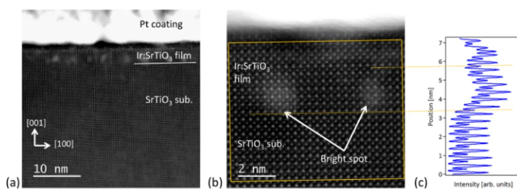
Figure 2.Cross-sectional HAADF−STEM image of a 5% Ir-doped SrTiO3(10 u.c.) film on a SrTiO3(001) substrate. (a) Wide view and (b)
magnified view of the film observed along the [010] zone axis. (c) HAADF intensity profile in the marked square region integrated along the horizontal direction (parallel to the substrate interface).
ACS Omega Article
DOI:10.1021/acsomega.7b02071
ACS Omega 2018, 3, 2169−2173
3. RESULTS AND DISCUSSION
Oscillations of the RHEED specular spot intensity observed during the deposition of an Ir:SrTiO3film are shown inFigure 1a. Clear oscillations can be observed for at last 10 u.c., which indicates that the growth proceeded in a layer-by-layer mode.19 However, the intensity of the oscillations clearly decreases. Because thefilm surface retains a step-and-terrace morphology, as shown by the AFM image inFigure 1b, we can conclude that the oscillation intensity drop is not associated with a spread of the crystal growth front over several unit cell layers but is instead related to the local surface roughness increase during the growth of an Ir-doped SrTiO3film.
An abrupt change in the intensity oscillations occurs after 300 s, at afilm thickness of 6 u.c. This type of specular intensity phase shift has been associated with a change of the surface termination of the film.20 Because the chemically etched substrate surface is initially terminated by the TiO2layer, we can assume that during the growth of thefirst five u.c., the film retains the perovskite B-site TiO2termination.Figure 1b shows
the morphology of thefilm surface after the growth of four u.c. Clearly, the step-and-terrace surface morphology of the SrTiO3 substrate was replicated on thefilm surface. Because the growth of nondoped SrTiO3 proceeds under identical growth
conditions in a layer-by-layer mode for hundreds of u.c.,21 the surface change observed in Ir-dopedfilms thicker than 5 u.c. is most likely related to segregation of the Ir dopants.
Figure 2a shows a cross-sectional HAADF−STEM image of a 10 u.c. thick Ir:SrTiO3 film taken along the [010] zone axis. The perfect match between the film and the substrate lattice, better observed in Figure 2b, shows that the film is fully epitaxial and coherent with the SrTiO3substrate. The images show several bright spots, about 1 nm in size, in the Ir-doped film. These bright spots are all located at the same depth from the surface within the first five u.c. of the film. Figure 2c presents an intensity profile of the atomically resolved HAADF image displayed in Figure 2b, integrated over a direction parallel to the interface. It shows that the presence of the bright spots causes a contrast blurring that does not affect the atomic plane spacing but increases the background intensity. Such bright spots are commonly observed in HAADF−STEM images when transverse atomic displacements occur, originating from strain fields associated with dislocation cores or point defects.22In our case, the observed contrast is most probably caused by local enrichment with Ir atoms, favoring local structural distortions and, Ir being heavier than Ti, enhancing the Z-contrast (atomic number contrast) in the HAADF− STEM image.
The variation of the Ir concentration in different parts of the film was analyzed by acquiring EDX spectra in the square regions defined in the HAADF−STEM images shown inFigure 3. To distinguish the Ir Lα peak at 9.174 keV, the figure presents magnified regions of the EDX spectra in an energy range close to the Cu K peaks, which originate from the copper grid on which the sample was mounted. Comparison of the spectra shows that the Ir Lα peak has a much higher intensity in the bright spots (Figure 3a) than in the darker regions in which almost no Ir was detected (Figure 3b). A slight Ir enrichment is also observed in the vicinity of thefilm surface (Figure 3c,d). The evolution of the Ir peak intensity from the substrate toward thefilm surface is clearly observed in the line profile of the Ir Lα peak amplitude recorded across a bright spot and displayed inFigure 3d.
The bright spots are thus clearly associated with local Ir enrichment in regions that are 2−4 u.c. wide (about 0.8−1.5 nm). The bright spots appear to be well-separated, the projected distance between them being 2−8 nm for a ∼40 nm thick cross-sectional specimen.
The relative stability of Ir cations as a function of substitution of Ti octahedral site location in the film was investigated by DFT calculations. Three configurations with different Ir distributions were considered: with one Ir atom in each TiO2 surface layer (Figure 4 S), with one Ir atom in each TiO2
subsurface layer (Figure 4S-1), and with two Ir atoms in the same TiO2central atomic layer (Figure 4C). The results show
that for sufficiently low Ir doping levels, the positioning of the two Ir atoms at the surface (S) is energetically less stable by 0.59 eV than having the Ir atoms located in the subsurface layer (S-1) or in the center (C) of the slab. These two last configurations (S-1 and C) have the same stability as they give almost equal total energies with a difference of only 0.01 eV, confirming that, away from the surface, Ir atoms do not have any preferential location (far or near each other), as far as they
Figure 3.EDX spectra recorded at three different regions of the same 5% Ir-doped SrTiO3film giving evidence for a strong variation in the Ir
content. (a) Ir Lα peak measured at a bright spot, (b) Ir Lα peak measured in between bright spots, (c) Ir Lα peak measured close to the surface, and (d) line profile across a bright spot.
are located in an octahedral atomic site. This result agrees with our previous calculations performed on Ir-doped bulk SrTiO3.
18
The nature of the iridium atoms within thefilm and close to the surface was investigated using XPS. XPS spectra of the Ir 4f5/2 and 4f7/2 core level peaks are shown in Figure 5.
Deconvolution of the peak profile showed that the Ir:SrTiO3
film contained Ir4+and Ir0components. The inelastic mean free
path of photoelectrons in an XPS measurement using the Al Kα source is only a few nanometers, which means that the depth distribution of the Ir4+and Ir0components can be estimated by measuring spectra at different takeoff angles. Measurements closer to the surface normal direction can detect photoelectron emission from deeper layers than measurements done at lower takeoff angles, which are more surface-sensitive. Figure 5a,b shows Ir 4f peak profiles measured at 45° and 20° takeoff angles (as measured from the sample surface), respectively. The Ir0 ratio (∼13%) was higher in the more surface-sensitive spectrum taken at a takeoff angle of 20°. In comparison, the Ir0ratio was ∼10% for the 45° spectrum. Whereas tetravalent Ir4+ is
expected for iridium atoms substituted for Ti, as considered in the DFT calculations, metallic Ir0is observed. The Ir0content
difference between the two takeoff angles is small, and
considering the effective probing depth, metallic Ir0 is likely
to be present in the clusters observed by HAADF−STEM. This result suggests that clustering and the appearance of metallic Ir0already occurs for 5% doping and shows that the Ir dopant atoms are not homogeneously distributed among the Ti sites of the host SrTiO3lattice.
Ir is known to form macroscopic self-organized metallic nanopillars in SrTiO3 when films are grown by PLD at
intermediate oxygen pressures of around 1 mTorr.6 In the present study, thefilms were grown at 5 × 10⁻⁶Torr, a pressure which was assumed to yield homogeneously doped Ir:SrTiO3 films, where uniformly distributed Ir atoms occupy Ti sites of the SrTiO3lattice. However, whereas AFM images of thefilms showed no surface structures suggesting Ir segregation, atomically resolved HAADF−STEM images and associated EDX analyses gave evidence for the occurrence of segregation of the Ir atoms forming Ir-rich cluster in thefilms. A possible scenario can be derived from the obtained experimental results. The XPS spectra show that metallic Ir0is present in the film,
which means that Ir must occupy other lattice sites besides just replacing Ti. Because the films are grown at a low oxygen pressure of 5× 10⁻⁶Torr and oxygen vacancies thus exist in the lattice during growth, the most likely cluster formation scenario is the placement of Ir atoms at the oxygen site, forming a metallic defect in the crystal. It is known that under suitable thermodynamic and kinetic growth conditions, nanometer-scale fcc-type metallic Ir inclusions can form in Ir:SrTiO3. Most likely, the clusters observed in the HAADF−STEM images in this work are the initial seeds of such macroscopic metal inclusions.
The Ir-rich cluster size appears to be quite uniform, and the distribution of clusters in the growth direction is clearly not random. There are a large number of clusters in the HAADF− STEM image within thefirst five u.c., but no clusters can be found in the next three u.c. of thefilm. Considering the phase shift observed in the RHEED intensity oscillations, it appears that the cluster formation and growth are related to the surface composition of thefilm and the lateral diffusion rate of Ir on the surface.
4. CONCLUSIONS
We have shown that Ir-rich clusters form in Ir-doped SrTiO3
films during the initial growth phase. Although the formation of macroscopic Ir metallic inclusions in SrTiO3has been observed
before,6 the STEM−EDX analysis in this work shows that Ir clustering occurs on a unit cell scale even whenfilms are grown
Figure 4.Atomic structures used for calculations, two Ir atoms in 3× 3× 6.5 SrTiO3supercell (∼3.2% Ir): with one Ir atom in each TiO2
surface layer (S), with one Ir atom in each TiO2subsurface layer (S-1),
and with the two atoms in the same center TiO2atomic layer (C). The
relative energetic stability of the different configurations is shown for each configuration. The total energy of the most stable structure (C) is taken as a reference.
Figure 5.Ir 4f5/2and 4f7/2XPS spectra of a 5% Ir-doped SrTiO3film taken with an Al Kα X-ray source (1486.6 eV). The takeoff angle from the
sample surface was 45° in (a) and 20° in (b). The spectrum in (b) is more surface-sensitive.
ACS Omega Article
DOI:10.1021/acsomega.7b02071
ACS Omega 2018, 3, 2169−2173
at low oxygen pressures. Because the cluster size of 2−8 nm is below the AFM spatial resolution limit, such segregation is difficult to detect by surface morphology analysis. Even if no obvious surface segregation is seen by AFM, Ir clustering may still occur. We showed that the small clusters cannot be seen in surface topography but can be detected by STEM. This pointed out to the importance of combining topography analyses with XPS or STEM exploration to verify whether metal clustering occurs when synthesizing noble metal-doped perovskites for photo-electrochemical applications. The extent of the nano-clusters in the growth direction depends on a combination of thermodynamic (temperature and oxygen pressure) and kinetic (growth rate) factors. Wefind that the 5% doping level exceeds the solubility limit of homogeneous Ir:SrTiO3 in SrTiO3, as
shown by the XPS measurement, excess Ir segregation starting immediately at the initial growth stage. The mechanism studied here is expected to be an effective method for synthesizing photoelectrode materials based on noble metal nanoclusters supported in an oxide matrix. The application area of such materials is photo-electrochemical energy conversion.
■
AUTHOR INFORMATION Corresponding Authors*E-mail:lee.mihee.ld7@ms.naist.jp(Mihee Lee). *E-mail:mlippmaa@issp.u-tokyo.ac.jp(Mikk Lippmaa). ORCID
Mihee Lee:0000-0003-2351-164X Ryota Takahashi:0000-0003-2430-2444
Notes
The authors declare no competingfinancial interest.
■
ACKNOWLEDGMENTSThe work was partially supported by the NAIST Presidential Special Fund and by Grants-in-Aid for Scientific Research 26105002 and 17H04895 from the Japan Society for the Promotion of Science. This work was granted access to the HPC resources of CALMIP supercomputing center under the allocations p1313 and p1509 (2016−2017). The authors gratefully acknowledge Lucien Datas and Teresa Hungria for their assistance with the ARM200F at the UMS Castaing of Toulouse University and Robin Cours for his help with the TEM specimen preparation at CEMES.
■
REFERENCES(1) Ray, C.; Pal, T. Recent advances of metal−metal oxide nanocomposites and their tailored nanostructures in numerous catalytic applications. J. Mater. Chem. A 2017, 5, 9465−9487.
(2) Liu, X.; Iocozzia, J.; Wang, Y.; Cui, X.; Chen, Y.; Zhao, S.; Li, Z.; Lin, Z. Noble metal−metal oxide nanohybrids with tailored nanostructures for efficient solar energy conversion, photocatalysis and environmental remediation. Energy Environ. Sci. 2017, 10, 402− 434.
(3) Munnik, P.; de Jongh, P. E.; de Jong, K. P. Recent Developments in the Synthesis of Supported Catalysts. Chem. Rev. 2015, 115, 6687− 6718.
(4) Shiraishi, Y.; Yasumoto, N.; Imai, J.; Sakamoto, H.; Tanaka, S.; Ichikawa, S.; Ohtani, B.; Hirai, T. Quantum tunneling injection of hot electrons in Au/TiO2 plasmonic photocatalysts. Nanoscale 2017, 9,
8349−8361.
(5) Wang, D.; Hisatomi, T.; Takata, T.; Pan, C.; Katayama, M.; Kubota, J.; Domen, K. Core/Shell Photocatalyst with Spatially Separated Co-Catalysts for Efficient Reduction and Oxidation of Water. Angew. Chem., Int. Ed. 2013, 52, 11252−11256.
(6) Kawasaki, S.; Takahashi, R.; Yamamoto, T.; Kobayashi, M.; Kumigashira, H.; Yoshinobu, J.; Komori, F.; Kudo, A.; Lippmaa, M. Photoelectrochemical water splitting enhanced by self-assembled metal nanopillars embedded in an oxide semiconductor photoelectrode. Nat. Commun. 2016, 7, 11818.
(7) Nishihata, Y.; Mizuki, J.; Akao, T.; Tanaka, H.; Uenishi, M.; Kimura, M.; Okamoto, T.; Hamada, N. Self-regeneration of a Pd-perovskite catalyst for automotive emissions control. Nature 2002, 418, 164−167.
(8) Zhang, W.; Ramesh, R.; MacManus-Driscoll, J. L.; Wang, H. Multifunctional, self-assembled oxide nanocomposite thin films and devices. MRS Bull. 2015, 40, 736−745.
(9) Zaera, F. Nanostructured materials for applications in heterogeneous catalysis. Chem. Soc. Rev. 2013, 42, 2746−2762.
(10) Yoshida, M.; Takanabe, K.; Maeda, K.; Ishikawa, A.; Kubota, J.; Sakata, Y.; Ikezawa, Y.; Domen, K. Role and Function of Noble-Metal/ Cr-Layer Core/Shell Structure Cocatalysts for Photocatalytic Overall Water Splitting Studied by Model Electrodes. J. Phys. Chem. C 2009, 113, 10151−10157.
(11) Hou, X.; Takahashi, R.; Yamamoto, T.; Lippmaa, M. Microstructure analysis of IrO2 thin films. J. Cryst. Growth 2017,
462, 24−28.
(12) Kiss, B.; Manning, T. D.; Hesp, D.; Didier, C.; Taylor, A.; Pickup, D. M.; Chadwick, A. V.; Allison, H. E.; Dhanak, V. R.; Claridge, J. B.; Darwent, J. R.; Rosseinsky, M. J. Nano-structured rhodium doped SrTiO3-Visible light activated photocatalyst for water
decontamination. Appl. Catal., B 2017, 206, 547−555.
(13) Blöchl, P. E. Projector augmented-wave method. Phys. Rev. B: Condens. Matter Mater. Phys. 1994, 50, 17953−17979.
(14) Kresse, G.; Hafner, J. Ab initio molecular-dynamics simulation of the liquid-metal−amorphous-semiconductor transition in germa-nium. Phys. Rev. B: Condens. Matter Mater. Phys. 1994, 49, 14251− 14269.
(15) Kresse, G.; Furthmüller, J. Efficient iterative schemes for ab initio total-energy calculations using a plane-wave basis set. Phys. Rev. B: Condens. Matter Mater. Phys. 1996, 54, 11169−11186.
(16) Monkhorst, H. J.; Pack, J. D. Special points for Brillouin-zone integrations. Phys. Rev. B: Solid State 1976, 13, 5188−5192.
(17) Perdew, J. P.; Burke, K.; Ernzerhof, M. Generalized Gradient Approximation Made Simple. Phys. Rev. Lett. 1996, 77, 3865−3868.
(18) Lee, M.; Arras, R.; Warot-Fonrose, B.; Hungria, T.; Lippmaa, M.; Daimon, H.; Casanove, M. J. Strain induced atomic structure at the Ir-doped LaAlO3/SrTiO3interface. Phys. Chem. Chem. Phys. 2017,
19, 28676−28683.
(19) Lippmaa, M.; Nakagawa, N.; Kawasaki, M.; Ohashi, S.; Koinuma, H. Growth mode mapping of SrTiO3 epitaxy. Appl. Phys.
Lett. 2000, 76, 2439−2441.
(20) Matvejeff, M.; Chikyow, T.; Lippmaa, M. Interface growth of La1.2Sr1.8Mn1.7Ru0.3O7Ruddlesden−Popper films on SrTiO3. J. Cryst.
Growth 2009, 311, 1201−1205.
(21) Ohnishi, T.; Shibuya, K.; Yamamoto, T.; Lippmaa, M. Defects and transport in complex oxide thin films. J. Appl. Phys. 2008, 103, 103703.
(22) Muller, D. A.; Nakagawa, N.; Ohtomo, A.; Grazul, J. L.; Hwang, H. Y. Atomic-scale imaging of nanoengineered oxygen vacancy profiles in SrTiO3. Nature 2004, 430, 657−661.
![Figure 2a shows a cross-sectional HAADF − STEM image of a 10 u.c. thick Ir:SrTiO 3 fi lm taken along the [010] zone axis.](https://thumb-eu.123doks.com/thumbv2/123doknet/13692010.432533/4.938.510.822.97.677/figure-shows-cross-sectional-haadf-stem-image-srtio.webp)

