3D printed multiplexed electrospinning sources for large-scale
production of aligned nanofiber mats with small diameter spread
The MIT Faculty has made this article openly available.
Please share
how this access benefits you. Your story matters.
Citation
García-López, Erika et al. “3D Printed Multiplexed Electrospinning
Sources for Large-Scale Production of Aligned Nanofiber Mats with
Small Diameter Spread.” Nanotechnology 28, 42 (September 2017):
425302. © 2017 IOP Publishing Ltd
As Published
http://dx.doi.org/10.1088/1361-6528/aa86cc
Publisher
IOP Publishing
Version
Final published version
Citable link
http://hdl.handle.net/1721.1/112243
Terms of Use
Attribution 3.0 International (CC BY 3.0)
Nanotechnology
PAPER • OPEN ACCESS
3D printed multiplexed electrospinning sources for
large-scale production of aligned nanofiber mats
with small diameter spread
To cite this article: Erika García-López et al 2017 Nanotechnology 28 425302
View the article online for updates and enhancements.
Related content
Parallel nanomanufacturing via electrohydrodynamic jetting from microfabricated externally-fed emitter arrays
Philip J Ponce de Leon, Frances A Hill, Eric V Heubel et al.
-Fabrication of aligned nanofibers by electric-field-controlled electrospinning: Insulating-block method
Wontae Hwang, Changhyun Pang and Heeyeop Chae
-Electrospray-printed nanostructured graphene oxide gas sensors
Anthony P Taylor and Luis F Velásquez-García
-3D printed multiplexed electrospinning
sources for large-scale production of aligned
nano
fiber mats with small diameter spread
Erika García-López
1,2, Daniel Olvera-Trejo
1and
Luis F Velásquez-García
2,31
Tecnológico de Monterrey, Escuela de Ingeniería y Ciencias, Ave. Eugenio Garza Sada 2501, Monterrey, N.L., 64849, México
2
Microsystems Technology Laboratories, Massachusetts Institute of Technology, 77 Massachusetts Ave., Cambridge, MA, 02139, United States of America
E-mail:Velasquez@alum.mit.edu
Received 30 June 2017, revised 11 August 2017 Accepted for publication 17 August 2017 Published 18 September 2017
Abstract
We report the design, fabrication, and characterization of novel, low-cost, and modular miniaturized nanofiber electrospinning sources for the scalable production of non-woven aligned nanofiber mats with low diameter variation. The devices are monolithic arrays of electrospinning emitters made via stereolithography; the emitters are arranged so each element has an independent line of sight to a rotating collector surface. Linear and zigzag emitter packing were evaluated using a PEO solution with the aim of maximizing the throughput of nanofibers with the smallest diameter and narrowest distribution. Current versusflowrate characterization of the devices showed that for a given flowrate a zigzag array produces more current per emitter than a linear array of the same emitter pitch and array size. In addition, the data demonstrate that larger and denser arrays have a net gain inflow rate per unit of active length. Visual inspection of the devices suggests uniform operation in devices with as many as 17 emitters with 300μm inner diameter and 1.5 mm emitter gap. Well-aligned nanofiber mats were collected on a rotating drum and characterized; the 17-emitter device produced the same narrow nanofiber distribution (∼81 nm average diameter, ∼17 nm standard deviation) for all tested flow rates, which is strikingly different to the performance shown by 1-emitter sources where the averagefiber diameter significantly increased and the statistics notably widened when the flowrate increases. Therefore, the data demonstrate that massively multiplexing the emitters is a viable approach to greatly increase the throughput of non-woven aligned nanofiber mats without sacrificing the statistics of the nanofibers generated. The production of dry nanofibers by the 17-emitter array is estimated at 33.0 mg min−1(1.38 mg min−1per mm of active length), which compares favorably with the reported multiplexed electrospinning arrays with emitters distributed along a line. Keywords: 3D printing, electrospinning, high-throughput nanomanufacturing, multiplexed electrospray sources, nanofibers
(Some figures may appear in colour only in the online journal)
1. Introduction
Electrospinning is a physical process in which ultrathinfibers are generated via electrohydrodynamic jetting. The feedstock is usually composed of long-chain polymers dissolved in a polar solvent, whereby the solvent evaporates during the
Nanotechnology Nanotechnology 28(2017) 425302 (12pp) https://doi.org/10.1088/1361-6528/aa86cc
3
Author to whom any correspondence should be addressed.
Original content from this work may be used under the terms of the Creative Commons Attribution 3.0 licence. Any further distribution of this work must maintain attribution to the author(s) and the title of the work, journal citation and DOI.
spinning process while the jet generated travels from the electrospinning emitter to a collector [1]. The jet is mainly
subject to two forces with opposing effects[2], i.e., (i)
elec-trostatic repulsion of the charges in the jet that decreases the fiber diameter, and (ii) surface tension pulling that tries to break up the jet into droplets. If the viscosity of the liquid is high enough and thefluid contains long-chain molecules the electrostatic repulsion prevails, resulting in a jet with very small diameter that becomes afilament after drying. The fiber morphology is controlled by parameters such as the applied electric field, the distance between the emitter and the col-lecting substrate, temperature, flow rate, humidity, and properties of the feedstock including the polymer dissolved, concentration, surface tension, conductivity, and viscosity[3];
in general, these parameters are interrelated.
Non-woven aligned nanofiber mats are of great interest in applications that exploit the arrangement of the fibers, e.g., directionally reinforced nanocomposites with enhanced mechanical or thermal properties, biomedical applications where cell proliferation is improved by the aligned layering of the fibers. In particular, biomedical devices such as tissue engi-neering scaffolds, drug release devices, and biochemical sensors require a biocompatible surface material such as polylactic acid [4], polyethylene oxide (PEO) [5,6], polyvinyl alcohol (PVA)
[7,8], chitosan [9,10], chitosan with PEO [11–15],
polylactic-co-glycolic acid-chitosan with PVA [16], and chitosan with
PVA[17] to achieve cell proliferation. Electrospun nanofibers
can be collected into non-woven mats withfibers layered aligned using structured electrode collectors [18] or a rotating surface
[19]. In the latter approach, several collector designs including
drum, wire drum, and disc collectors[20] have been adapted to
produce nanofibers in various biomaterials, e.g., PVA and PEO [21,22]. A rotating drum aligns nanofibers based on the
tan-gential speed of the collector surface; when the surface speed is smaller than the alignment speed, thefibers are deposited ran-domly[23]. However, fiber breakage may occur if the rotating
speed is excessively high[24].
Manufacturing unwoven nanofiber mats at a high produc-tion rate remains a challenge. Some efforts have focused on modifying the collector design[24], expanding the number of
emitters [20,25–32], and increasing the flow rate [33];
none-theless, multi-emitter designs have proven more effective than increasing theflow rate [28]. The multi-nozzle electrospinning
sources reported in the literature can be classified by the way of supplying the feedstock: there are systems with spouts fed individually through syringes[25–27,29,32], and multi-nozzle
systems where the feedstock is driven from a common reservoir to each nozzle [28, 31]. The maximum emitter density in a
multiplexed electrospinning source is influenced by the emitter pitch and the emitter geometry. For example, Varesano et al[27]
described an array of up to nine emitters with 2 cm emitter pitch distributed in two columns. In contrast, Yamashita et al[28] and
Tomaszewski et al [31] reported a minimum gap between
emitters of 3 mm; a smaller spacing caused merging of the jets from adjacent emitters into droplets.
Microfabricated multiplexed electrospinning sources have also been explored to increase nanofiber throughput [34]. Microfabrication technology can circumvent some of the
manufacturing challenges faced by these systems including the tight control of the dimensions, the monolithic creation of the emitter arrays with the feedstock supply network, and the miniaturization of the emitters to achieve larger emitter den-sity and operation at less bias voltage. In particular, Ponce de Leon et al reported a planar electrospinning emitter array made of silicon via deep reactive-ion etching with 225 emitters spaced 2 mm[35].
Additive manufacturing, i.e., the layer-by-layer construction of devices using a computer-aided design(CAD) file [36], has
been recently explored as a manufacturing toolbox for micro-systems. Researchers have shown 3D printed devices with per-formance on par or better than counterparts made with standard microfabrication [37, 38], and also demonstrated designs not
previously attainable due to fabrication complexity[39,40]. In
addition, the manufacturing time and cost of a complex 3D printed microfluidic system are significantly less than those incurred in traditional microfabrication, making possible to iterate multiple times the design and to satisfy a wider range of commercial applications.
This work reports novel 3D printed multiplexed electro-spinning sources for scalable production of aligned nanofibers with low diameter distribution using a rotating drum as collector. The devices were made via digital light processing-stereo-lithography (DLP-SLA), which is an additive manufacturing technology that creates solid objects by photopolymerization of a liquid resin [36]. DLP-SLA can create freeform objects with
cavities at high resolution. The 3D printed devices were char-acterized using a PEO solution as feedstock. Per-emitter current versus emitterflowrate data were acquired for devices with dif-ferent emitter packing, emitter density, and array size, looking to maximize theflow rate per axial length of collector. In addition, metrology was conducted on non-woven aligned nanofiber mats created using different devices and emitterflow rates in a home-built rotating drum apparatus to determine the conditions for high-throughput generation of thin, uniformfibers.
2. Methods and materials
2.1. Feedstock
PEO(Mw = 900 000) and deionized water (DI) were purchased from Sigma-Aldrich (Sigma-Aldrich, USA). PEO fibers were spun from 4 wt% PEO in DI water; the PEO solution was created by adding PEO to the DI water while stirring at 80°C for 3 h; the solution was cooled down and conserved at room temperature overnight before being used. According to Jin et al a 4 wt% PEO solution in DI water at the same molecular weight has a viscosity of∼1.25 Pa s at a shear rate of ∼100 s−1[41].
The use of PEO in this study is motivated by its bio-compatibility [42] and remarkable performance for cell
pro-liferation in nanofiber membranes [43]. Fong et al investigated
that higher viscosity and a reduced surface tension favor the formation offibers without beads [44].
2.2. Device design
The devices used in this study have the emitters spatially arranged so that each element has an independent line of sight to a rotating drum or a roll-to-roll manufacturing setup. Two packing configurations were explored: in the linear arrays the emitters are distributed along a straight line, while in the zigzag arrays the emitters are distributed along a line twisting around a straight line. For the same emitter pitch the zigzag devices(figure1(a)) have half the projected emitter pitch (i.e.,
emitter gap) of the linear arrays (figure 1(b)); therefore, a
zigzag array has twice the emitters per unit of length of a linear array with the same emitter pitch. This is significant because the closer the emitters are, the weaker the electric field acting on the emitter tips is, which decreases the current produced per emitter and even inhibits emission. Zigzag arrays of 3, 7, 9, 11, 13, 17, 21, and 25 emitters and linear arrays of 1, 7, and 9 emitters were manufactured; in each array, the maximum distance between the outermost emitters is equal or smaller than 24 mm, and the emitter gap varied between 12 mm and 1 mm.
The 3D printed multiplexed electrospinning sources have a rectangular body with a length of 38.67 mm, a width of 24.25 mm, and a height of 15.25 mm(measured from the central inlet to the spouts). The design consists of a 1.56 mm diameter central inlet (figure 1(c)) that supplies the feedstock into an
internal tank with a total height of 3 mm a length of 31.25 mm and a width of 12 mm. The feedstock tank is internally rein-forced by an array of 1.5 mm wide square columns to provide support to the ceiling of the 3D printed structure; the columns
have a 500μm radius fillet on both ends for a smooth liquid distribution. A horizontal 900μm wide microfluidic channel in zigzag is embedded into the ceiling of the tank and serves as manifold to distribute the feedstock to a series of vertical feed meandering coils; each coil delivers feedstock to a different emitter and acts as a hydraulic impedance that ballasts the emitter. The coils are uniformly tapered, with an inlet diameter of 900μm, decreasing to 700 μm at the outlet. The shape of the coils maximizes the emitter density and minimizes the device volume (in a planar array, the feed coils would be helical as in[39]).
Each emitter has a 4 mm-tall conical body with a dia-meter at the base equal to 1.9 mm and a diadia-meter at the top (spouts) equal to 1.6 mm; the geometry of the emitter elim-inates in many cases the merging of the jets (see section4).
Each emitter has a vertical tapered channel at the center with an inlet diameter equal to 700μm and a diameter at the spout equal to 300μm, which is the minimum feature size of the multiplexed electrospinning source proposed in this study. The tapered hydraulics makes the filling-in pressure lower than the dripping pressure(i.e., the pressure needed to break the menisci at the emitter spouts), facilitating the supply of feedstock to all the emitters before activation.
2.3. Device manufacturing
The devices were made with the low-cost (<$3500), high-resolution DLP-SLA 3D printer Solus and the resin Solu-sProto (Junction 3D, Santa Clarita, CA, USA); the printer uses a modified commercial DLP projector as UV source. Each design wasfirst created as a parametric model using the commercial software SolidWorks 2015 (DS SolidWorks Corporation, Waltham, MA, USA); the model was then
Figure 1.(a) 3D schematic of a 3D printed source with 17 emitters arranged in zigzag with 3 mm emitter pitch, i.e., 1.5 mm gap between emitters;(b) top-view schematic of a linear array with 9 emitters and a gap between emitters of 3 mm; (c) lateral cross section of a linear array —the cross section passes through the axes of the emitters.
3
converted to a 3D meshfile in STL format with a resolution of 2μm, i.e., an order of magnitude smaller than the pixels of the 3D printer. After that, thefile is processed by the software Contour(Junction 3D, Santa Clarita, CA, USA), transforming the 3D mesh into 25μm tall slices that are communicated to the printer and the projector. The printer creates, layer by layer, the solid object by polymerizing the resin at the bottom of the vat with UV light patterned by the projector; the printed object is attached to a build platform that moves back and forth within the vat, replenishing the resin at the bottom of the vat and correcting the amplitude of the movement as the printing job progresses. After the printing process is com-pleted, the device is detached from the platform using pliers in twisting motion to avoid scratching the surface of the platform. The cleaning process consists in immersing the device twice in isopropyl alcohol(IPA) for 5 min, replacing the bath in between. A bottle with a dispensing needle is connected to the inlet of the device and IPA is pressure fed, removing the uncured resin from the channels; unlike most SLA resins that are gooey, the resin SolusProto has water-like viscosity, which greatly facilitates the cleaning operation. The channels are blown using compressed dry air(CDA) fed to the inlet of the device, and the IPA/air channel purge operation is repeated until visually confirming that no more uncured resin is coming out of the device and that all the emitters are ejecting uniformly IPA when the inlet of the device is fed with a dispensing needle. Finally, the devices are dried with CDA and put in a UV curing chamber (XYZ printing, San Diego, CA, USA) for 10 min.
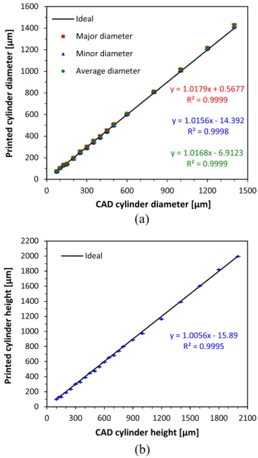
Previously to print the electrospinning sources, resolution matrices were printed and measured to assess the capabilities of the printer and the resin(figure2). The resolution matrices
were plates with arrays of vertical cylinders spanning a range of diameters and heights; the diameters of the cylinders were varied between 75 and 1400μm in multiples of the printer pixels(25 μm), while the heights of the cylinders were varied between 100 and 2000μm in multiples of the slicing height (also 25 μm). Cylinders with diameters larger or equal to 200μm were measured using a Mitutoyo Quick Vision ACTIVE 202 optical microscope with a 1.5X objective lens and 100 nm resolution, while the cylinders with diameters smaller than 200μm were measured with a Leica Micro-systems’ research-grade microscope incorporated with the Renishaw Invia Reflex Raman Confocal Microscope system equipped with a motorized stage for area mapping with in-plane step sizes of 100 nm and vertical step size of 16 nm. For each combination of diameter and height, 35 nominally identical cylinders were measured. The metrology shows close correspondence between the dimensions of the CAD models and the printed objects. The printed heights of the cylinders are about 0.6% larger than the CADfile and have an offset of 16μm (about one slice), while the printed diameters are about 1.7% larger than the CADfile and have an offset of 7μm (smaller than a pixel). The average standard deviation of the in-plane and out-of-plane features is 7μm and 0.5 μm, respectively.
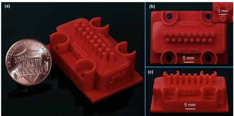
Figure3 shows a 3D printed 17-emitter electrospinning source with zigzag emitter packing:figure3(a) is an isometric
view of the device next to a one-cent US coin as comparison, figure3(b) is a top view of the device with a close-up view of
a cluster of emitters, andfigure3(c) is the lateral view of the
device. The volume of the device is 6.95 cm3, costs∼$2 in printable material, and takes∼60 min to print.
3. Experimental setup
3.1. Emitted current versus flow rate characterization
Figure4(a) is a schematic of the experimental setup used to
collect current versus flow rate characteristics from the 3D printed devices. The apparatus supplies feedstock to the device, biases voltages to the device and to a collector elec-trode, measures the current emitted by the device, and allows forfine adjusting of the separation between the emitter spouts
Figure 2.Metrology of resolution matrices printed with the Solus 3D printer and the SolusProto resin:(a) printed diameter versus CAD diameter,(b) printed height versus CAD height.
and the collector electrode. In the setup, the miniaturized multiplexed electrospinning source is clamped to an alumi-num chuck using M4 nylon screws; the top surface of the chuck has a groove with an O-ring that surrounds an orifice; when clamped, the bottom of the device squeezes the O-ring to make a watertight connection between the inlet of the device and the liquid feed. The chuck is secured to a vertical translation stage VAP10(Thorlabs, Newton, NJ, USA) using a polypropylene sheet mounted on an aluminum breadboard fixed with 90° mounting adapters. The vertical stage is attached on an aluminum base plate protected with poly-propylene sheets to insulate thefixture. The distance between the collector electrode and the emitter spouts is controlled using afine adjustment knob with a resolution of 1.27 mm per revolution. A syringe pump NE-1000 (New Era Pump Sys-tems Inc., Farmingdale, NY, USA) supplies PEO solution at differentflow rates through a central flangeless nut made of PFA resin(IDEX Health & Science LLC, Oak Harbor, WA, USA), which was screwed to the back of the aluminum chuck. The aluminum chuck is electrically grounded.
A 4 inch wide stainless-steel square electrode positioned 8 cm away from the emitter spouts was covered with an aluminum foil sheet to collect the nanofibers. A bias voltage of−20 kV with respect to the aluminum chuck was applied to the collector electrode using a dual output high-voltage power supply (Gamma High Voltage, Ormond Beach, FL, USA). The current emitted by the device was measured using a picoammeter 485 Keithley(Tektronix, Cleveland, OH, USA) and data signals were recorded using an oscilloscope DS6104 (Rigol, Beaverton, OR, USA). Also, an external 5 MΩ high-voltage resistor (Newark, Chicago, IL, USA) was used to protect the picoammeter in the event of an electric short.
In a typical experiment the device was first tested dry to verify electrical insulation between the device and the collector electrode; an average leakage current of 0.77 nA was measured, which is over two orders of magnitude smaller than any of the currents measured in the wet experiments. The devices were then fed with PEO solution at a given flow rate and the total current was measured after visually confirming that a Taylor cone on each spout was formed; the current was very stable during the acquisition time. Theflow rate was varied and a new current measurement was conducted, until a given flow rate range was covered. The per-emitter current and per-emitterflow rate were estimated by dividing the corresponding quantities by the number of emitters of the device. The experiments were monitored with a 5 MP CCD color digital camera attached to a 12X zoom microscope lens. After running experiments, the device wasflushed with DI water to remove any leftover feed-stock within the device;finally, the device was dried with CDA and stored for future reuse.
3.2. Aligned nanofiber collection and metrology
After current versus flow rate characterization, selected 3D printed devices were used to generate non-woven aligned nanofiber mats using the apparatus shown in figure4(b). In
the setup, the 3D printed electrospinning source is secured to the aluminum chuck described in section3.1. Also, the PEO solution was supplied by the syringe pump to the device while a bias voltage of 20 kV with respect to the collector electrode was applied to the chuck using a dual output high-voltage power supply. The collector electrode is a rotating drum that is grounded, i.e., the polarity and magnitude of the bias voltage in the aligned nanofiber collection experiments are identical to those of the current versusflow rate experiments.
Figure 3.(a) Optical image of a 3D printed device with 17 emitters in zigzag near a one-cent US coin as comparison; (b) top-view of the device showing the zigzag packing of the emitters and close-up view of a cluster of emitters;(c) lateral view of the device evidencing the conical shape of the nozzles.
5
The emitters are aligned with respect to the axis of the drum, and the separation between the emitter spouts and the edge of the drum was set at 8 cm (i.e., the separation used in the current versusflow rate characterization).
The rotating drum collector subsystem consists of a 4 inch diameter aluminum cylinder mounted on electrically insulated bearings that are secured to a 0.75 inch thick che-mical-wear resistant sheet by using nylon screws and PTFE washers; the drum is rotated by a DC motor with a controller (McMaster-Carr, Robbinsville, NJ, USA). A 6 inch wide and 0.125-in thick horizontal polyethylene plate was positioned at the drum height to prevent the generation of an air cushion around the collector surface that inhibits the collection of the nanofibers on the surface of the drum. The DC motor con-troller uses a potentiometer to set the angular speed of the drum as a percentage of the maximum rotation frequency. Rotating the drum at 75% of the maximum rotation frequency (i.e., at 43.1 Hz or 13.8 m s−1 tangential speed), resulted in
collecting well-aligned nanofibers; in contrast, a drum speed equal to 25% or 50% of the maximum rotation frequency resulted in misaligned fibers, and a drum speed higher than 80% of the maximum rotation frequency caused high
amplitude vibrations due to a natural frequency of the struc-ture, resulting infiber breakage.
The chuck and rotating drum subsystem are enclosed in a desiccator with pressure-controlled nitrogen flow feed (Terra Universal Inc., Fullerton CA, USA) to control the relative humidity during the collection of the nanofiber mats. A temperature and relative humidity sensor EasyLog data logger (Dataq Instruments Inc., Akron, OH, USA) was installed inside the chamber to monitor the relative humidity and temperature during the experiments. Preliminary studies were conducted to define the optimal nitrogen flow pressure and relative humidity for depositing the nanofibers, resulting in 20 psi nitrogen pressure and 20% relative humidity, respectively.
Preliminary studies were conducted to select the collector surface material; a repeatable collection of aligned nanofibers was achieved directly on the aluminum drum surface. The nanofiber mats were carefully retrieved from the surface of the drum and placed on a SEM pin stub mount, to then be coated with a 10 nm thick carbon coating using a Q150T Turbo-Pumped Sputter Coater (Quorum Technologies, Sacramento, CA, USA). Afterward, samples were measured with a Merlin Carl Zeiss SEM(Zeiss, Germany) with a 3 kV accelerating voltage. For each device tested, aligned nanofiber mats were collected for different flow rates. For each flow rate, metrology of 100 diameter fiber measurements was performed to obtain fiber size distributions. Fiber diameters were measured by ImageJ software (National Institute of Health, Bethesda, MD, USA) drawing parallel lines along the edges of the fibers and measuring the distance between the lines. The histograms were calculated using categories from 20 to 25 nm and around 5–9 bin sizes across the distribution.
4. Experimental results and discussion
4.1. Per-emitter current versus flow rate characteristics
Table 1 summarizes the geometry specifications of the dif-ferent zigzag and linear devices tested with the maximum flow rate per emitter, per device, and per device’s active length(i.e., 24 mm, which is the useful length of the internal feedstock tank; the active length is what would be tiled in a longer device) that was achieved on each device while operating uniformly(figure5). The data suggest that there is a
trend of achieving smaller maximum per-emitterflow rates in devices with smaller emitter gap; however, the device with the largest flow rate and flow rate per unit of active length correspond to the largest array size with the smallest emitter gap. In other words, a device with larger emitter gap increases the maximum flow rate that can be sprayed by each emitter, while a device with larger array size increases the totalflow ejected by the device, with a net gain in total flow rate for larger/denser arrays. For a given device, feeding a larger emitter flow rate than the quoted maximum caused dripping, which eventually led to jet merging and non-uniform jet operation. In all cases, 1 ml h−1was the minimum per-emitter
Figure 4.(a) Experimental setup used for measuring current versus flow rate characteristics; (b) experimental apparatus used to collect non-woven mats of aligned nanofibers.
flow rate that resulted in the stable generation of a jet from each emitter.
It was not possible to activate simultaneously all emitters of the zigzag arrays with 21 (2.4 mm emitter pitch) or 25 emitters(2 mm emitter pitch) at any flow rate without having the jets merging or dripping, or having intermittent operation of the emitters; we hypothesize that the small emitter pitch
made the electricfield acting on the emitter tips too low for the formation of a stable jet per emitter. Although Liu et al reported formation of multiple jets from an emitter between dripping events[45], such fiber generation mechanism is less
attractive because it does not efficiently use the feedstock. The intermittent emitter operation was also observed by Tomasweski et al in arrays of emitters with small emitter separation[31].
Figure 6 shows the per-emitter current versus flow rate characteristics of various multiplexed electrospinning sources with different number of emitters, emitter pitch, and emitter packing. In all the experiments, there is a good correspon-dence between the data and a least-square power-law fit where the per-emitter current is roughly proportional to the square root of the per-emitterflow rate. Figure6(a) shows the
per-emitter current versus flow rate characteristics of a 1-emitter device, a 7-emitter linear array with 4 mm pitch/ gap, a 7-emitter zigzag array with 4 mm pitch/2 mm gap, a 9-emitter linear array with 3 mm pitch/gap, and a 9-emitter zigzag array with 6 mm pitch/3 mm gap. Three interesting trends are shown in the figure: (i) for the same per-emitter flow rate, the devices with a plurality of emitters produce less per-emitter current than the 1-emitter device, evidencing a reduction in the electric field on the emitter spouts due to shadowing by the adjacent emitters;(ii) for a given flow rate per emitter, a zigzag array produces more current per emitter than a linear array of the same emitter pitch and array size; (iii) for dense enough arrays, making the array denser/larger does not significantly reduce the per-emitter current; in addition, each kind of emitter packing seems to converge to a different limit characteristic.
Figure6(b) shows the per-emitter current versus flow rate
characteristics of various zigzag devices, i.e., multiplexed electrospinning sources with 3, 7, 11, and 13 emitters with 4 mm emitter pitch(2 mm emitter gap), and a 17-emitter array with 3 mm emitter pitch (1.5 mm emitter gap). The data suggest that arrays with the same emitter pitch and larger array size emit less per-emitter current, down to a certain limit characteristic. However, the data also suggest that the limit
Table 1.Summary of specifications of tested 3D printed multiplexed electrospun nanofiber sources.
Array
packing Array size
Emitter pitch(mm)
Emitter gap(mm)
Maximumflow rate per emitter(ml h−1)
Maximumflow rate per device(ml h−1)
Maximumflow rate per devi-ce’s active length (ml h−1mm−1) Linear 1 — — 5.00 5.0 0.21 Linear 7 4 4 5.00 35.0 1.46 Zigzag 7 4 2 3.50 24.5 1.02 Linear 9 3 3 4.00 36.0 1.50 Zigzag 9 6 3 4.00 36.0 1.50 Zigzag 3 4 2 5.00 15.0 0.63 Zigzag 11 4 2 4.00 44.0 1.83 Zigzag 13 4 2 3.25 42.3 1.76 Zigzag 17 3 1.5 2.75 46.8 1.95 Zigzag 21 2.4 1.2 — — — Zigzag 25 2 1 — — —
Figure 5.Examples of 3D printed multiplexed electrospinning sources in uniform operation:(a) 9-emitter zigzag array with 6 mm emitter pitch(i.e., 3 mm emitter gap); (b) 9-emitter linear array with 3 mm emitter pitch(i.e., 3 mm emitter gap). When working uniformly, one stable jet per emitter is generated.
7
per-emitter current versusflow rate characteristic varies with the emitter density, i.e., for a given flow rate a device with less distance between emitters (i.e., denser arrays) produce less per-emitter current.
In this study, the largest and densest arrays that con-tinuously operated uniformly had 17 emitters with 1.5 mm emitter gap, which also emitted the largest totalflow rate and totalflow rate per unit of active length while delivering up to 2.75 ml h−1 per emitter (table 1); in addition, the device
produced the smallest emitter current for a given per-emitterflow rate. Moreover, the 13-emitter zigzag array with 4 mm emitter pitch was able to deliver almost three times the maximum flow rate ejected by the 3-emitter array with the same emitter packing and pitch. Therefore, the data support the conclusion that multiplexing the emitters is a viable approach to increase the total throughput of electrospinning sources.
4.2. Nanofiber characterization
The non-woven mats of aligned nanofibers were collected using 4 different 3D printed devices(a 1-emitter source, and zigzag arrays with 1.5 mm emitter gap and 3, 7, and 17 emitters) while ejecting three different per-emitter flow rates (i.e., 1 ml h−1, 1.5 ml h−1 and 2 ml h−1); examples of
well-aligned nanofiber mats are shown in figure7, while the his-tograms from the metrology of the nanofibers are shown in figure8grouped per device; a summary of the corresponding statistics is shown in table2. For the 1-emitter source(figure8
(a)), the mode diameter is 75 nm and the distributions fairly narrow for flow rates equal to 1 ml h−1 and 1.5 ml h−1; however, for 2 ml h−1, the mode becomes 175 nm and dis-tribution greatly widens with a right-skewed trend. Even though the 1-emitter source can eject significantly more flow rate, the data suggest operating at the lower end of theflow rate range to achieve the thinnest fibers with the narrowest distribution.
Figures8(b)–(d) show the fiber diameter distribution for
various zigzag arrays with 1.5 mm emitter gap. In all cases, the average diameter enlarges with an increment of the flow rate, but the increase and spread is less pronounced than in the
Figure 6.Per-emitter current versusflow rate characteristics for various arrays. In the plots, x L is a linear array with x emitters, and x ZZ is a zigzag array with x emitters. In a linear array the emitter gap and pitch are the same, in a zigzag array the emitter gap is half the emitter pitch. Infigure6(b), the least-square fit of the 11-emitter and 13-emitter zigzag arrays with 2 mm emitter gap was jointly calculated.
Figure 7.Examples of aligned nanofibers generated from a 1-emitter source(a), (b) and zigzag arrays with 1.5 mm emitter gap and 3 (c), (d), 7(e), (f), and 17 (g), (h) emitters while flowing 1 ml h−1per emitter.
1-emitter case. Moreover, the 17-emitter array produced for practical purposes the same tight nanofiber distribution (∼81 nm average mean diameter, ∼17 nm average standard deviation) at all flow rates tested in the experiments. Therefore, the data demonstrate that massively multiplexing the emitters in an electrospinning source is a viable approach to greatly increase the throughput of non-woven aligned nanofiber mats without sacrificing the statistics of the nanofibers generated.
Figure 9 shows the dispersity (i.e., ratio between the standard deviation and the arithmetic average) of the nanofi-ber diameter distributions of the zigzag arrays with 3, 7, and
17 emitters shown infigure8. In general, the devices with 3 and 7 emitters produce nanofibers with larger dispersity than the device with 17 emitters, although there is no clear trend of which device has associated the smallest dispersity for a given per-emitter flow rate (the 3-emitter device, 7-emitter device, and 17-emitter device have associated the smallest dispersity at 1 ml h−1, 1.5 ml h−1, and 2 ml h−1 per-emitter flow rate, respectively). Nonetheless, the grouping of the dispersity for the 17-emitter device is the tightest,fluctuating around 22% and changing little across the range offlow rates tested. We hypothesize that the difference in the statistics between 3, 7,
Figure 8.Statistical distribution of the nanofiber diameters generated by different electrospinning sources at different per-emitter flow rates: (a) 1-emitter source, (b) 3-emitter zigzag array (c) 7-emitter zigzag array, (d) 17-emitter zigzag array. All the zigzag arrays had 1.5 mm emitter gap.
Table 2.Summary of statistical results of the nanofiber measurements.
1.0 ml h−1 1.5 ml h−1 2.0 ml h−1
Array
packing Array size
Emitter gap(mm) Average dia-meter(nm) Standard deviation
(nm) Average dia-meter(nm)
Standard deviation
(nm) Average dia-meter(nm)
Standard deviation (nm) Linear 1 — 62.79 14.38 72.32 25.69 197.39 53.32 Zigzag 3 1.5 64.08 11.7 64.06 23.32 80.57 25.62 Zigzag 7 1.5 67.39 22.37 82.72 22.35 105.72 18.07 Zigzag 17 1.5 77.29 19.83 84.31 16.72 83.25 17.39 9 Nanotechnology 28(2017) 425302 E García-López et al
and 17-emitter arrays is probably due to the differences in per-emitter current. Infigure6(b), the data suggest that arrays
with the same emitter pitch and larger array size emit less per-emitter current for a givenflow rate; larger per-emitter current implies larger Coulomb repulsion, causing stronger whipping of the jet, resulting in more statistical variation of the diameter of the nanofiber. In addition, in figure 6(b) the slope of the
per-emitter current versus flow rate characteristic is smaller for arrays with the same emitter pitch and larger array size; therefore, differences in the emitterflow rate across the array affect less the uniformity of the emitter current across the array in devices with larger array size. Consequently, the 17-emitter array produces more uniform nanofibers because it has associated the smallest per-emitter current for a given flow rate and the mildest slope of the per-emitter current versusflow rate characteristic.
High-throughput generation of aligned nanofibers is essential to satisfy commercial applications. Parallel emitters distributed along a line have been proposed to increase system productivity; however, to the best of our knowledge this is the first report on multiplexed sources that create mats of aligned nanofibers. For example, Tomaszewski and Szadkowski [31]
reported three configurations of stainless steel electrospinning heads that produced PVA nanofibers, i.e., a 26-emitter linear array(75 mm active length), a 26-emitter elliptical array along the perimeter of an ellipse with semi-axes equal to 110 and 60 mm(545.7 mm active length), and a 10-emitter concentric array distributed around the perimeter of a 50 mm diameter circle (157.1 mm active length). The linear array was dis-carded because only the emitters at the ends of the array were operational; however, the elliptical head produced a total mass flow rate of 11 mg min−1 (0.02 mg min−1 per mm of active length), and the concentric head produced a total mass flow rate per emitter of 12 mg min−1(0.08 mg min−1per mm
of active length). Also, Wang et al reported melt jet electro-spinning of polyethylene using an aluminum blade(140 mm active length) that generates 20–25 jets to produce a total flow rate of 80 mg min−1 [46] (0.57 mg min−1 per mm of active length). Based on the data and the measured density of the PEO solution(1060 kg m−3), the maximum mass flow rate of
dryfibers that the 17-emitter source can produce is estimated at 33.0 mg min−1(1.94 mg min−1per emitter or 1.38 mg min−1 per mm of active length). If the active length of the 17-emitter device would be tiled on the 0.5 m-long active length of the commercial free-surface electrospinning source NS 1S500U Nanospider (ELMARCO, Czech Republic), the total flow rate of the source would be∼974 ml h−1, i.e., it would deplete the 500 ml standard tank in about 31 min, which is 16 times faster than their average continuous run[47].
5. Conclusions
This study demonstrated novel, low-cost, 3D printed, minia-turized, multiplexed electrospinning sources for generation in great quantities of non-woven aligned nanofiber mats using a rotating drum as collector. Two emitter packing versions were investigated: linear arrays, i.e., devices with the emitters deployed along a straight line, and zigzag arrays, i.e., devices with emitters distributed along a line twisting around a straight line. Current versus flowrate characterization of the devices shows that for a given flow rate, a zigzag array pro-duces more current per emitter than a linear array of the same emitter pitch and array size; also, for dense enough arrays, making the array larger does not significantly reduce the per-emitter current.
The largest and densest arrays that continuously operated uniformly, with no dripping, had 17 emitters with 1.5 mm emitter gap, which also ejected the largest totalflow rate and totalflow rate per unit of active length while delivering up to 2.75 ml h−1 per-emitter. The 17-emitter array produced the same tight nanofiber distribution (∼81 nm average diameter, ∼17 nm standard deviation) at all flow rates tried in the experiments (1–2 ml h−1 per emitter); this is strikingly dif-ferent to the performance shown by 1-emitter sources where the average fiber diameter significantly increased and the statistics notably widened for increasingflow rate. Therefore, the data demonstrate that massively multiplexing the emitters is a viable approach to greatly increase the throughput of non-woven aligned nanofiber mats without sacrificing the statistics of the nanofibers generated. The production of dry nanofibers of the 17-emitter array is estimated at 33.0 mg min−1, 1.94 mg min−1 per emitter, or 1.38 mg min−1 per mm of active length, which compares favorably with the reported multiplexed arrays with emitters distributed along a line.
Several directions for future work on 3D printed multi-plexed electrospinning sources are identified. First, without changing the 3D printing technology, the electrospinning sources could be made of more resilient materials, e.g., ceramic [48], to be chemically compatible with a greater
variety of feedstock. Second, the emitters could include more complex geometries, e.g., coaxial spouts [39] for hollow
nanofiber generation. Third, the great flexibility of the DLP-SLA printing process can yield devices with multi-feedstock feeds; these devices could alternate emitters ejecting different materials that blend into the non-woven mat a plurality of properties, e.g., mechanical reinforcement, self-healing,
Figure 9.Dispersity of the data from the zigzag arrays with 3, 7, and 17 emitters shown infigure8.
transduction, electrical conduction, and cooling, to implement smart nanostructured textiles.
Acknowledgments
This research has been funded in part by the MIT-Tecnológico de Monterrey Nanotechnology Program. The authors would like to thank Emil Karapetian from Junction 3D for his help in the printing aspects of the work, and Zhumei Sun from Mas-sachusetts Institute of Technology for conducting the metrology of the 3D printed resolution matrices.
ORCID iDs
Erika García-López https: //orcid.org/0000-0002-3341-298X
Daniel Olvera-Trejo https: //orcid.org/0000-0002-4385-6269
Luis F Velásquez-García https: //orcid.org/0000-0002-9232-1244
References
[1] Larrondo L and Manley R S J 1981 Electrostatic fiber spinning from polymer melts: 1. Experimental-observations onfiber formation and properties J. Polym. Sci. B9 909–20 [2] Doshi J and Reneker D H 1995 Electrospinning process and
applications of electrospunfibers J. Electrost.35 151–60 [3] Burger C, Hsiao B S and Chu B 2006 Nanofibrous materials
and their applications Annu. Rev. Mater. Res.36 333–68 [4] Ou K L, Chen C S, Lin L H, Lu J C, Shu Y C, Tseng W C,
Yang J C, Lee S Y and Chen C C 2011 Membranes of epitaxial-like packed, super aligned electrospun micron hollow poly(l-lactic acid) (PLLA) fibers Eur. Polym. J.47 882–92 [5] Deitzel J M, Kleinmeyer J D, Hirvonen J K and Beck Tan N C
2001 Controlled deposition of electrospun poly(ethylene oxide) fibers Polymer42 8163–70
[6] Shin Y M, Hohman M M, Brenner M P and Rutledge G C 2001 Experimental characterization of electrospinning: the electrically forced jet and instabilities Polymer42 9955–67 [7] Koski A, Yim K and Shivkumar S 2004 Effect of molecular
weight onfibrous PVA produced by electrospinning Mater. Lett.58 493–7
[8] Ding B, Kim H Y, Lee S C, Lee D R and Choi K J 2002 Preparation and characterization of nanoscaled poly(vinyl alcohol) fibers via electrospinning Fibers Polym.3 73–9
[9] Siridamrong P, Phrotjanatharee P and Thamronganaskul N 2016 Chemical crosslinking of silkfibroin, chitosan and gelatin blend nanofiber mats Key Eng. Mater.695 273–7
[10] Xu F, Weng B, Gilkerson R, Materon L A and Lozano K 2015 Development of tannic acid/chitosan/pullulan composite nanofibers from aqueous solution for potential applications as wound dressing Carbohydrate Polym.115 16–24 [11] Kriegel C, Kit K M, McClements D J and Weiss J 2009
Electrospinning of chitosan–poly(ethylene oxide) blend nanofibers in the presence of micellar surfactant solutions Polymer50 189–200
[12] Zhang Y Z, Su B, Ramakrishna S and Lim C T 2008 Chitosan nanofibers from an easily electrospinnable UHMWPEO-doped chitosan solution system Biomacromolecules9
136–41
[13] Ojha S S, Stevens D R, Hoffman T J, Stano K, Klossner R, Scott M C, Krause W, Clarke L I and Rusell E G 2008 Fabrication and characterization of electrospun chitosan nanofibers formed via templating with polyethylene oxide Biomacromolecules9 2523–9
[14] Bhattarai N, Edmondson D, Veiseh O, Matsen F A and Zhang M 2005 Electrospun chitosan-based nanofibers and their cellular compatibility Biomaterials26 6176–84 [15] Subramanian A, Vu D, Larsen G F and Lin H Y 2005
Preparation and evaluation of the electrospun chitosan/PEO fibers for potential applications in cartilage tissue
engineering J. Biomater. Sci.16 861–73
[16] Duan B, Yuan X, Zhu Y, Zhang Y, Li X, Zhang Y and Yao K 2006 A nanofibrous composite membrane of PLGA–chitosan/ PVA prepared by electrospinning Eur. Polym. J.42 2013–22 [17] Huang X J, Ge D and Xu Z K 2007 Preparation and
characterization of stable chitosan nanofibrous membrane for lipase immobilization Eur. Polym. J.43 3710–8 [18] Li D, Wang Y and Xia Y 2004 Electrospinning nanofibers as
uniaxially aligned arrays and layer-by-layer stackedfilms Adv. Mater.16 361–6
[19] Wang S-H, Wan Y, Sun B, Liu L-Z and Xu W 2014 Mechanical and electrical properties of electrospun PVDF/ MWCNT ultrafine fibers using rotating collector Nanoscale Res. Lett.9 522–8
[20] Zhou F L, Gong R H and Porat I 2009 Mass production of nanofibre assemblies by electrostatic spinning Polym. Int.58 331–42
[21] Niu H, Lin T and Wang X 2009 Needleless electrospinning: I. A comparison of cylinder and disk nozzles J. Appl. Polym. Sci.114 3524–30
[22] Tang S, Zeng Y and Wang X 2010 Splashing needleless electrospinning of nanofibers Polym. Eng. Sci.50 2252–7
[23] Huang Z M, Zhang Y Z, Kotaki M and Ramakrishna S 2003 A review on polymer nanofibers by electrospinning and their applications in nanocomposites Compos. Sci. Technol.63
2223–53
[24] Teo W E and Ramakrishna S 2006 A review on electrospinning design and nanofibre assemblies Nanotechnology17 R89
[25] Kim G, Cho Y S and Kim W D 2006 Stability analysis for multi-jets electrospinning process modified with a cylindrical electrode Eur. Polym. J.42 2031–8 [26] Yang E, Shi J and Xue Y 2010 Influence of electric field
interference on double nozzles electrospinning J. Appl. Polym. Sci.116 3688–92
[27] Varesano A, Rombaldoni F, Mazzuchetti G, Tonin C and Comotto R 2010 Multi-jet nozzle electrospinning on textile substrates: observations on process and nanofibre mat deposition Polymer Int.59 1606–15
[28] Yamashita Y, Ko F, Miyake H and Higashiyama A 2008 Establishment of nanofiber preparation technique by electrospinning Sen’i Gakkaishi64 24–8
[29] Theron S A, Yarin A L, Zussman E and Kroll E 2005 Multiple jets in electrospinning: experiment and modeling Polymer
46 2889–99
[30] Yang Y, Jia Z, Li Q, Hou L, Gao H, Wang L and Guan Z 2006 Multiple jets in electrospinning IEEE 8th Int. Conf. on Properties & applications of Dielectric Materialspp 940–3
[31] Tomaszewski W and Szadkowski M 2005 Investigation of electrospinning with the use of a multi-jet electrospinning head Fibres Textiles East. Eur.13 22–6
[32] Bowman J, Taylor M, Sharma V, Lynch A and Chadha S 2011 Multispinneret methodologies for high throughput electrospun nanofiber MRS Proc.752 AA1.5.1–.5
[33] Zargham S, Bazgir S, Tavakoli A, Rashidi A S and
Damerchely R 2012 The effect offlow rate on morphology and deposition area of electrospun nylon 6 nanofiber J. Eng. Fabr. Fibers7 42–9
11
[34] Srivastava Y, Marquez M and Thorsen T 2007 Multi-jet electrospinning of conducting nanofibers from microfluidic manifolds J. Appl. Polymer Sci.106 3171–8
[35] Ponce de Leon P J, Hill F A, Heubel E V and
Velásquez-García L F 2015 Parallel nanomanufacturing via electrohydrodynamic jetting from microfabricated
externally-fed emitter arrays Nanotechnology26 225301 [36] Vaezi M, Seitz H and Yang S 2013 A review on 3D
micro-additive manufacturing technologies Int. J. Adv. Manuf. Technol.67 1721–54
[37] Velásquez-García L F 2015 SLA 3D-printed arrays of miniaturized, internally-fed, polymer electrospray emitters J. Microelectromech. Syst.24 2117–27
[38] Gong H, Woolley A T and Nordin G P 2016 High density 3D printed microfluidic valves, pumps, and multiplexers Lab Chip16 2450–8
[39] Olvera-Trejo D and Velásquez-García L F 2016 Additively manufactured MEMS multiplexed coaxial electrospray sources for high-throughput, uniform generation of core-shell microparticles Lab Chip16 4121–32
[40] Skylar-Scott M A, Gunasekaran S and Lewis J A 2016 Laser-assisted direct ink writing of planar and 3D metal
architectures PNAS113 6137–42
[41] Jin H J, Fridrikh S V, Rutledge G C and Kaplan D L 2002 Electrospinning Bombyx mori Silk with Poly(ethylene oxide) Biomacromolecules3 1233–9
[42] Lee J H, Lee H B and Andrade J D 1995 Blood compatibility of polyethylene oxide surfaces Prog. Polym. Sci.20
1043–79
[43] Lou C W, Lin J H, Yen K C, Lu C T and Lee C Y 2008 Preparation of polyethylene oxide/chitosan fiber membranes by electrospinning and the evaluation of biocompatibility Textile Res. J.78 254–7
[44] Fong H, Chun I and Reneker D H 1999 Beaded nanofibers formed during electrospinning Polymer40 4585–92 [45] Liu C K, Chen M Y, Sun R J, Zhang W H, Zhang Z H and
Yao M 2010 Experimental investigation on the multiple jets from a single droplet by electrospinning Adv. Mater. Res.
129–131 365–9
[46] Wang Q, Curtis C K, Muthuraman Thoppey N, Bochinski J R, Gorga R E and Clarke L I 2014 Unconfined, melt edge electrospinning from multiple, spontaneous, self-organized polymer jets Mater. Res. Express1 045304
[47] http: //elmarco.com/nanofiber-equipment/electrospinning-machines-ns1s500u/(Accessed: 10 August 2017)