HAL Id: ird-00403290
https://hal.ird.fr/ird-00403290
Submitted on 23 Aug 2009
HAL is a multi-disciplinary open access
archive for the deposit and dissemination of
sci-entific research documents, whether they are
pub-lished or not. The documents may come from
teaching and research institutions in France or
L’archive ouverte pluridisciplinaire HAL, est
destinée au dépôt et à la diffusion de documents
scientifiques de niveau recherche, publiés ou non,
émanant des établissements d’enseignement et de
recherche français ou étrangers, des laboratoires
Capillary microchannel fabrication using plasma
polymerized TMDS for fluidic MEMS technology
Abdennour Abbas, Philippe Supiot, Vianney Mille, Didier Guillochon,
Bertrand Bocquet
To cite this version:
Abdennour Abbas, Philippe Supiot, Vianney Mille, Didier Guillochon, Bertrand Bocquet. Capillary
microchannel fabrication using plasma polymerized TMDS for fluidic MEMS technology. Journal of
Micromechanics and Microengineering, IOP Publishing, 2009, 19, pp.045022. �ird-00403290�
Capillary microchannel fabrication using plasma polymerized
TMDS for fluidic MEMS technology
Abdennour Abbas
1,2,3, Phlippe Supiot
2, Didier Guillochon
3, Bertrand Bocquet
11 Institute of Electronic, Microelectronic and Nanotechnology (UMR CNRS 8520). University of Lille1, FR 2 Laboratory of Process Engineering of Reactive fluids-Materials Interactions (EA 3571), University of Lille1, FR
3 Laboratory of Biological Processes, Enzymatic and Microbial Engineering (EA 1026), University of Lille1, FR
E-mail: [email protected]
Abstract. This paper reports the first use of cold plasma deposition of polymerizable monomers for the fast, cost effective
and easy fabrication of buried air-microchannels. A new method named “plasma polymerization on sacrificial layer” (PPSL) is presented. It consists in the direct polymerization of tetramethyldisiloxan (TMDS) on a photopatterned sacrificial layer. Channels are formed with only one lithographic mask and without any etching or bonding process. The use of polymerized TMDS allows a rapid creation of capillarity-driven flow systems with channels width ranging from 4 to 700 µm without pillars. Channels are characterized and successfully tested. Capillary forces draw water, as well as aqueous solution into the channel from the inlet reservoir to the outlet one, avoiding the need of microfluidic connectors with the surrounding environment. Filling of the capillaries is very fast. It reaches the initial velocity of 4.4 cm.s–1 with the
geometries and water used here. In addition, PPSL easily allows the building of transparent channel networks directly on processed electrochemical or electromagnetic components. An example of a such integrated fluidic MicroElectroMechanical System (MEMS) is described.
PACS. 42.82.Cr Fabrication techniques; lithography, pattern transfer – 85.85.Va Micromachining – 64.70.km Polymers –
85.85.+j Micro- and nano-electromechanical systems (MEMS/NEMS) and devices.
1. Introduction
Over the last decade, the need for rapid and low cost channel microfabrication methods is becoming increasingly important. Microchannels found their utility in three main topics: the integrated circuit technology, through the use of air gaps in interconnect structures for the reduction of the dielectric constant
[1], the microfluidic cooling of high density integrated circuits [2], the investigation of fluid mechanics on the microscale [3], and their applications in microfluidic devices including bio- and chemical-MEMS, biosensors and lab-on-chip [4], [5].
Many different techniques have been reported for the fabrication of microfluidic circuits. The most prevalent are the etching techniques [6], [7], replication methods based essentially on molding [8], [9] and sacrificial material approach [10]. The main drawback common
to both the etching methods and polymer molding techniques is the small flexibility for different substrate materials, the need of several photolithographic mask which multiply time consuming steps and the need of aligning and bounding process of different fabricated layers. This step usually requires thermal or chemical treatment and can lead to wafer-to-wafer misalignments [11]. A unique technology that permits a rapid and easy fabrication of microchannels on one side of the silicon wafer is the sacrificial material approach. In this method, microchannel fabrication begins with deposition of the sacrificial layer and patterning into the desired shape. The structural material is then deposited over the micropatterned sacrificial layer, except in a small area which will provide an access to the sacrificial material. The later is then dissolved chemically or thermally or by plasma etching, leaving a covered channel. Several materials have been used as
Published in the Journal of Micromechanics and Microengineering
J. Micromech. Microeng. 19 (2009) 045022 (8pp)
doi:10.1088/0960-1317/19/4/045022
ird-00403290, version 1 - 23 Aug 2009
sacrificial layer, including photosensitive materials such as electronic photoresists [12], thermally decomposable materials such as polycarbonates [13], polyoxymethylene [14], polynorbornene [15], [16], Parylene [17], and water soluble materials like poly(acrylic acid) and polyvinylalcohol [18].
Different sacrificial materials were widely investigated in the literature, while the amount of studies exploring new methods or materials for the overcoat layer remains relatively very low. Today, the most used technique to fabricate the overcoat material is a chemical vapour deposition (CVD) of silicon dioxide (SiO2), silicon nitride (SiNx) [19], [20], silicon carbide
(SiC) or different metals such as aluminium (Al), nickel (Ni) and titanium (Ti) [21], [22]. These materials are deposited at relatively high temperatures (≥ 200 °C). This requires the use of materials with high thermal stability and high glass transition temperatures. It also implies the use of adhesion layers. These constraints limit dramatically the number of materials that can be used. Here, we describe the realization and characterization of a simple process for buried air-microchannel fabrication. An alternative technology called Plasma Polymerization on Sacrificial Layer (PPSL) is introduced. It refers to the use of plasma polymerization to deposit the overcoat material in a process at ambient temperature.
The Plasma polymerization considered here is essentially a Remote Plasma Enhanced Chemical Vapour Deposition (RPECVD). It consists in the conversion of organic and/or organometallic monomers into highly cross-linked polymers through partial decomposition activated by energetic plasma species. This polymerization is accompanied by a subsequent deposition of thin films on the substrate. The primary advantage of the present plasma polymerization is that it can occur at moderate temperatures compared to conventional plasma deposition methods. This allows the use of a large panel of materials as sacrificial or encapsulating layers. The benefits of plasma polymerized films arise from their high biocompatibility, good adhesion on different substrates and very interesting surface properties either for microfluidic flows or for functionalization [23], [24].
2. Experimental procedure
2. 1. Microchannel fabrication
The fabrication process starts with a standard photolithography, with a two-step spin-coating process (Figure 1). First, the sacrificial material consisting of a positive photoresist (AZ9260, Hoechst) is spun-coated
Table 1.Process conditions of the photoresist AZ9260.
Process step Conditions
Spin coating 1 (AZ 9260) Speed: 2000 rpm, Acceleration: 5000 rpm, 40 sec Stabilization: 10 min. Soft-bake: 100 °C , 3 min
Water reabsorption: 15 min at room temperature Spin coating 2 (AZ 9260) Speed:2000 rpm, Acceleration: 5000 rpm, 40 sec Stabilization: 10 min. Soft-bake 3 min at 100 °C Water reabsorption: 15 min
UV exposure 10,48 mW/cm2 @ 365 nm (I-line), 45 sec
Development AZ 351 b (30 %), 90 sec Soft-bake 1 min at 100 °C Film thickness ~ 25 µm
Table 2.Process parameters of the Plasma polymerization of TMDS.
Base pressure 0.028 mbar Operating pressure 5.6 mbar
Power 200 W
Plasmagenic gas N2 : 1.8 slpma
carrier gas O2 : 25 sccmb
Pre-treatment N2 Plasma during 4 min,
followed by N2/O2 plasma
during 3min.
Treatment TMDS Plasma : 5 sccm
aslpm: standard liter per minute,
bsccm: standard cubic centimeter per minute
in two steps on the p-doped silicon wafer (100). The spin parameters and the viscosity of the polymer solution control the thickness of the deposited layer which determines the height of the air-channel (Table 1). The deposited photoresist is then cured to evaporate the solvent. This step is followed by UV exposure at 365 nm for a dose of 10 mJ.cm-2, through a high-resolution photomask featuring the microchannels. Areas not exposed to UV light are dissolved by immersion of the wafer in a basic solution, such as AZ 351B, leaving only a patterned sacrificial layer on the substrate. The microchannels were designed as 10 to 700 µm wide, 10 to 25 µm high and 3 mm long.
The following step is the deposition of the overcoat layer over the micropatterned surface. For the first, a plasma polymerization technology was integrated to a microelectronic fabrication process for the deposition of the encapsulating material. The wafer with desired structures was introduced into the reaction chamber of a home-built microwave (2.45 GHz) plasma reactor
[25]. Then, the organosilicon monomer 1,1,3,3,TetraMethylDiSiloxane (TMDS) was used as the precursor to synthetize and deposit a polymer organosilicon film by a remote afterglow PECVD. The deposited polymer, so called plasma polymerized
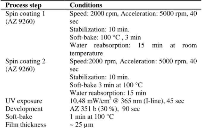
Figure 1.Principle of the PPSL process using two methods. Method 1 requires three main steps: (a) Micropatterning of the sacrificial material. The mask and the dose of UV exposure determine the shape of the patterns, (b) plasma polymerization of TMDS on the sacrificial layer, and (c) The decomposition of the sacrificial material leading to the release of a desired channel. Method 2 allows the fabrication of small channels without etching the sacrificial material. The distance between two patterns (L) governs the shape and the type of the microchannel obtained. It is to note that the SEM image (at the right) represent two hydrophobic microchannels, while the corresponding scheme show only one.
Figure 2.Infrared spectrum of plasma polymerized TMDS. (a) Semi developed formula of TMDS monomer.
TMDS (ppTMDS) is used as the structural material of the microchannel. Figure 2 shows the principal species composing the polymer. It was deposited at room
temperature at a rate of 14 nm.s-1. This technique is described in more details elsewhere [26], and the optimized conditions are summarized in Table 2. In the last step, the sacrificial layer is removed by immersion of the substrates into AZ351B developer (1:4) prepared with deionized water. The sacrificial photoresist decomposes into volatile and soluble products leaving behind a hollow channel. The resulting microchannels are optically transparent. Typical ppTMDS channels on Si substrate are shown in Figure 3. The released structures are rinsed in deionized water then underwent a supercritical CO2
drying to avoid the sticking effect caused by capillary forces.
2. 2. MEMS design and fabrication
PPSL technique was used to fabricate a BioMicroElectro Mechanical System (BioMEMS). This fabrication aims to demonstrate the feasibility of the direct integration of microfluidic circuits onto a
Figure 3.SEM micrographs of the cross-sectional view of microchannels resulting from the PPSL process before (a1, b1) and after (a2, b2) the etching of the sacrificial layer. (c) Circular-shape microchannel. (d) Top view optical micrograph of two parallel microchannels during the sacrificial material decomposition. The gray part represents the remaining photoresist and the clear area is the released channel after 30 min of etching.
Figure 4.Schematic representation of the microfabrication process of a fluidic MEMS. (A) photolithography of the coplanar waveguides on a silicon wafer: (1) deposition of a gold layer (2) Spin coating of the photoresist, (3) standard photolithography, (4, 5) Ion polishing and oxygen plasma treatment, (B) PPSL technique: starting with surface micropatterning of a sacrificial photoresist (steps 1 and 2), followed by the direct polymerization of TMDS monomer (step 3) and the decomposition of the sacrificial material (step 4).
substrate supporting electromagnetic components, here a coplanar wave guide (CPW). The later is used in high frequency circuits as propagation lines for dielectric and TeraHrertz spectroscopies [27], [28]. Figure 4 shows the proposed fabrication process. The CPW fabrication requires three steps. First, a thin layer of 200 nm Chromium (Cr) was sputtered over a high resistivity (5-10 Ω.cm-1) Si substrate as adhesion layer, before the deposition of 1 µm gold layer using Plassys MP 450S. Next, the substrate underwent a standard photolithography to transfer CPW features onto the gold layer. Then, the exposed gold areas are removed by ion polishing leaving the desired waveguides. The substrate is finally cleaned by oxygen plasma treatment.
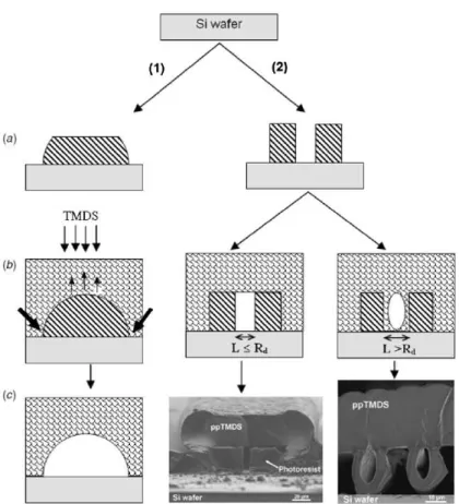
The integration of the microfluidic circuits is achieved by the plasma polymerization technique discussed above. The microchannels were designed as 130 to 700 µm wide, 25 µm deep and 3 mm long. Two channel ends were broadened to 1 mm to form open reservoirs for easier fluidic access (Figure 5). These reservoirs are masked during the plasma polymerization of the cover layer. There are subsequently used as etch holes of the sacrificial layer.
2. 3. Water filling experiments
The wetting properties of different materials and their surface energies are controlled by angle contact measurements using a GBX Digidrop. Experiments to study the filling of the microchannels were carried out with DI water and phosphate buffer (0.02 M, pH 6.8) as test fluids. To allow flow visualization, the microchannel system was mounted on an optical microscope equipped with a CCD camera. Because ppTMDS is transparent, liquid flow inside microchannel may be observed and captured as digital movie files. The fluidic features were determined by manual frame-to-frame comparisons.
3. Results and discussion
3. 1. Plasma polymerization
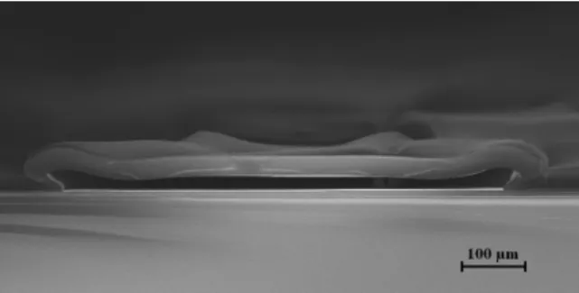
The ability to form a buried air microchannel requires specific properties for both the overcoat and the sacrificial materials. Here, PPSL technique was performed using plasma polymerized TMDS (ppTMDS) as the encapsulating material, and the positive photoresist AZ9260 as the sacrificial one. The ppTMDS deposit presents a good mechanical strength to span large air-gaps without collapsing during or after fabrication. Figure 6 shows a channel of 700 µm
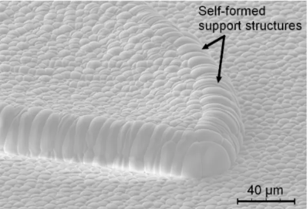
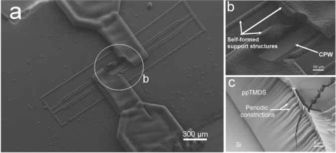
wide and 20 µm high without pillars. A variety of aspect ratios and channel sizes can be achieved with this method. This is made possible not only because of the mechanical strength of the polymer but also because of the special polymerization mode of the TMDS monomer at the edges of the micropatterned structures. In fact, it can be seen on Figure 7 that the film surface is formed by smooth and spherical hill-type morphologies of few micrometers size and the microchannel is surrounded by self-formed support structures. The laters play an important role to stabilize very large channels without pillars and also could explain the formation of periodic constrictions in the interior surface of ppTMDS channel side walls (Figure 8). These observations suggest that (i) the polymerization mechanism can be affected by surface micropatterning, leading to the appearance of some interesting features of the deposited films and (ii) the film grows by forming small spherical clusters on the surface. The polymerization parameters (input power, pressure, monomer flow rate) determine the size of these clusters which in turn probably determine the deposition resolution discussed below. Further investigations are needed to understand ppTMDS growth mechanism on patterned surface and its related properties.
Figure 5.SEM micrograph of a cross-sectional profile of the largest microchannel obtained by PPSL process. It presents dimensions of 700 µm width and 20 µm height.
Besides its topographical aspects, ppTMDS offers several advantages related to its physical and chemical properties, such as transparency in the visible wavelengths, chemical stability against solvents used in lithography process and a relative low permittivity (εr ≈ 4) with low losses in the millimeter wave and
terahertz spectrum [29]. The latter is of great interest for MEMS based on electromagnetic waveguides. Finally, unlike many polymers, ppTMDS is not self-fluorescent which enables self-fluorescent detection. The photoresist AZ9260 allows the achievement of a good aspect ratio and the deposition of film thickness up to
Figure 6.External aspect of a microchannel obtained by PPSL. The ppTMDS film surface is organized in spherical hill-type
morphologies of few micrometers size. Special features can be seen at the microchannel edges.
150 µm, corresponding to the achievable channel height [30]. However, PPSL is presently limited by the decomposition rate of this sacrificial material. Removing a polymerized AZ 9260 layer is the most time-consuming step, because the film polymerized during UV irradiation and becomes relatively highly cross-linked. The sacrificial polymer decomposes with initial rate of 7 µm/min into volatile and soluble products. This rate depends strongly on the channel dimensions, and decreases over time to 2 µm.min-1 because of the saturation of the etching solution. As a result, 10 hours are needed to release the fluidic circuit displayed in Figure 5. Longer decomposition times are required for longer and thicker microchannels. However, because of the chemical etching is a diffusion-limited process, there is a limitation in the length of the channel that can be processed. This hindrance can be overcome by the use of other sacrificial materials that can decompose within a reasonable time or that can be etched by plasma or thermal process. Video 1 in supplemental material shows the meniscus shape of water evaporating in the microchannel. The observed curvature confirms the hydrophobic properties of the channel wall after etching of the sacrificial layer, and ensures that there are negligible residues after decomposition. Figure 8 confirms that the microchannels are clean with no visible particulates contaminating the surface.
The direct plasma polymerization allows a good adhesion on a large variety of substrates, thus avoiding the use of additional adhesion layer. Furthermore, the deposition resolution (distance between two patterns that allows the deposition of the film on the support material, denoted Rd) of this method is estimated to be
around 4 µm. This property permits the fabrication of small channels (< 4µm width) without need of sacrificial materials. As we can see in Figure 1, the
plasma polymerization on predefined micropatterns leads to the appearance of hydrophobic closed channels whether the distance between these patterns is slightly higher than Rd. It is important to note that
the deposition resolution of the polymer could also be used to create small accesses in the sacrificial layer patterns (Figure 1, when L≤Rd) to allow the entering of
the etching solution and thus permit a faster decomposition.
3. 2. Microfluidic characterization
The ppTMDS microchannel is 2 mm long, 20 µm high and has a total volume of 23 nL. We designed two reservoirs at the ends of the channel. In addition to their role as access for the etching solution and as inlet/outlet ports, these reservoirs provide a surface tension that permits the filling of the channel by capillary force. The final device is shown in Figure 8. The system was filled by adding a droplet to the channel reservoir. Capillary forces dominate largely in microfluidic systems due to the large surface-to-volume ratio. Surface tension of a liquid meniscus provides sufficient pressure to push water into the channel. Water and buffer was drawn into the device by capillarity from one reservoir to another. Liquid flow inside micrometer-sized channels is essentially laminar (Reynolds number < 5 for the channel used here). In spiteof the hydrophobic feature of ppTMDS, there is no need to treat the surface to fill the channels, unlike other hydrophobic polymers such as PDMS based channels which need a prior hydrophilization treatment to allow positive capillary action [31]. This might be explained by three main factors:
(1) The capillary pressure produced by the liquid meniscus at the channel access reservoir allows water entering the microchannel. This pressure is described as follows [32], [33]:
++++
====
w
h
1
1
2
p
δ
( 1) Where w is the width of the channel, h its height, andthe surface tension δ(H2O) = 7,36.10-2 N.m-1 at 20 °C.
As the width of the reservoir is much larger than its thickness, equation (1) can be simplified to p = 2δ/h. The pressure difference at the entrance of the microchannel used here is then: p = 8.096. 107 Pa. This pressure draws water with initial velocity of V= 4.4 cm.s–1. The filling speed is reduced at the end to
V= 2.18 mm.s-1, due to the loss of pressure and viscosity effects. The filling speed is determined by the channel geometries, its surface energy and the liquid features.
Figure 7.SEM micrographs of the (a) fluidic MEMS, (b) Enlarged view of the partially abrased region, showing the electromagnetic sensor (CPW) and the self-formed support structures, (c) Interior surface of the ppTMDS channel side wall. We can see the periodic constrictions formed during polymerization.
(2) The internal walls of the ppTMDS channel present periodic constrictions of 1 to 2 µm width and height. These constrictions may favor capillarity effects and then promote the displacement of water-based solutions along channel surface [34]. This also can be useful in channel functionalization as these constrictions cause small velocities near the surface which in turn increases resident time and surface interactions, and thus promote adsorption and condensation of molecules.
(3) The inner walls of the microchannels are non-wettable. The only Si part is wettable, with the static contact angles θSi = 58° ± 3° and θppTMDS = 95° + 3°.
Total surface energies are 41.8 mJ.m-2 (dispersive component γd= 24.1 mJ.m-2, polar component γp= 17.7) and 22.3 mJ.m-2 (γd = 20.4 mJ.m-2, γp= 1.9 mJ.m
-2) for the hydrophilic and hydrophobic surfaces
respectively. Internal ppTMDS wall generates a positive pressure acting against filling, while surface tension force due to bottom hydrophilic silicon surface reduce the ppTMDS effect and assists the water to flow inside the microchannel. Other factors are already known to affect slip, including surface roughness and the reduction in channel width which acts as passive valves.
The water filling operation can be seen in Supplemental material (Video 2). Capillary pressure is used here as the simplest way to draw liquids on the
circuits. However, PPSL method can easily be applied to pressure driven flow systems and cavity based MEMS.
4. Conclusion
A novel fabrication method of closed microchannels for microfluidic systems is reported. It is based on a direct plasma polymerization of the encapsulating material, here the organosilicon polymer ppTMDS, on a photopatterned resist. The latter, used as a sacrificial layer, was then decomposed to release the desired channels. Using this technology, microchannels with various shapes and dimensions and with different surface features can be performed easily. In addition, this simple method allows the direct and rapid integration of fluidic circuits onto various sensors such as microelectrodes and waveguides.
Applying the concept of plasma polymerization to the fluidic MEMS fabrication is particularly attractive for several reasons: (1) it avoids the bonding step in the fabrication protocol; (2) it uses ambient temperature process; (3) the large panel of organic or organosilicon materials that can be deposited, (4) the good biocompatibility of these materials and their easy functionalization; (5) the processing onto different material substrates without the need of adhesion layer; (6) this process can be scaled up to industrial production relatively easily. Beside this, ppTMDS films enable the fabrication of very large cavities (>
700 µm) without pillars and small channels (< 5 µm width) without using a sacrificial material. One of our further challenges in this issue is the creation of microfluidic networks by the direct plasma polymerization of both sacrificial and overcoat layer to achieve the whole process in the same plasma reactor.
Acknowledgements
This work is supported by the National Research Agency funds (contract ANR-05-NT05-2_46562) and the Interdisciplinary Research Program of Lille University (PPF BioMEMS 2006 N° 1803).
References
[1] Kohl P A, Zhao Q, Patel K, Schmidt D, Allen S A B, Shick R, and Jayaraman S 1998 Air-Gaps for Electrical Interconnections Electrochem. Solid-State Lett. 1 49–51
[2] Dang B, Joseph P, Bakir M, Spencer T, Kohl P, Meindl J 2005 Wafer-level microfluidic cooling interconnects for GSI Proc.
of the IEEE International Interconnect Technology Conference, 6-8
June, p. 180–182, San Francisco (USA)
[3] Zhao B, Moore J S, Beebe D J 2001 Surface-Directed Liquid Flow Inside Microchannels Science 2911023–26
[4] Delamarche E, Bernard A, Schmid H, Michel B, Biebuyck H 1997 Patterned Delivery of Immunoglobulins to Surfaces Using Microfluidic Networks Science 276 779–781
[5] Treizebré A and Bocquet B 2008 Nanometric metal wire as a guide for THz investigation of living cells Int. J. Nanotechnol. 05 Nos. 6/7/8 784–95
[6] Boer M J d, Tjerkstra R W, Berenschot J W, Jansen H V, Burger G J, Gardeniers J G E, Elwenspoek M, and Van den Berg A 2000 Micromachining of Buried Micro Channels in Silicon IEEE J.
MEMS 9 94–103
[7] Dwivedi V K , Gopal R and Ahmad S 2000 Fabrication of very smooth walls and bottoms of silicon microchannels for heat dissipation of semiconductor devices Microelectron. J. 31 405–410
[8] Mcdonald J C And Whitesides G M 2002 Poly(dimethylsiloxane) as a material for fabricating microfluidic devices Acc. Chem. Res.35 491–499
[9] Chie R-D 2006 Micromolding of biochip devices designed with microchannels Sens. Actuators, A: Physical 128 238–247
[10] Peeni B A,Lee M L,Hawkins A R and Woolley A T 2006 Sacrificial layer microfluidic device fabrication methods
Electrophoresis 274888–4895
[11] Chatterjee R, Fayolle M, Leduc P, Pozder S, Jones B, Acosta E, Charlet B, Enot T, Heitzmann M, Zussy M, Roman A, Louveau O, Maitrejean S, Louis D, Kernevez N, Sillon N, Passemard G, Po V, Mathew V, Garcia S, Sparks T, Huang Z 2007 Three dimensional chip stacking using a wafer-to-wafer integration
International Interconnect Technology Conference, IEEE 4-6 June pp 81–83
[12] Walsh K, Norville J and Tai Y-C 2001 Photoresist as a sacrificial layer by dissolution in acetone The 14th IEEE
International Conference on Micro Electro Mechanical Systems,
p114 – 117
[13] Jayachandran J P, Reed H A, Zhen H, Rhodes L F, Henderson C L, Allen S A B, and Kohl P A, 2003 Air-Channel Fabrication for Microelectromechanical Systems via Sacrificial Photosensitive Polycarbonates IEEE J. MEMS 12 147–159
[14] L S and Gleason K K 2001 Hot filament chemical vapor deposition of polyoxymethylene as a sacrificial layer for fabricating air gaps Electrochem. Solid-State Lett. 4 G81–G84
[15] Bhusari D, Reed H A, Wedlake M, Padovani A M, Sue Ann Bidstrup Allen, and Kohl P A 2001 Fabrication of air-channel structures for microfluidic, microelectromechanical, and microelectronic applications IEEE J. MEMS 10 400–408
[16] Wu X, Reed H A, Wang Y, Rhodes L F, Elce E, Ravikiran R, Shick R A, Henderson C L, Allen S A B, and Kohl P A 2003 Fabrication of Microchannels Using Polynorbornene Photosensitive Sacrificial Materials J. Electrochem. Soc. 150 H205–H213
[17] Noha H-s, Choib Y, Wu C-f, Heskethaand P J, Allen M G 2003 Rapid, low-cost fabrication of parylene microchannels for microfluidic applications The 12th International Conference on Solid State Sensors, Actuators and Microsystems: Boston, June 8-12 [18] Linder V, Gates B D, Ryan D, Parviz B A, Whitesides G M
2005 Water-Soluble Sacrificial Layers for Surface Micromachining
Small 7 730–6
[19] Joseph P J, Kelleher H A, , Allen S A B and Kohl P A 2005 Improved fabrication of micro air-channels by incorporation of a structural barrier J. Micromech. Microeng. 15 35–42
[20] Peeni B A, Conkey D B, Barber J P, Kelly R T, Lee M L, Woolleya A T and Hawkins A R 2005 Planar thin film device for capillary electrophoresis Lab Chip 5 501–505
[21] Papautsky I, Brazzle J, Swerdlow H and Frazier A B 1998 A low-temperature IC-compatible process for fabricating surface-micromachined metallic microchannels IEEE J. MEMS 7 267–273
[22] Bagolini A, Pakula L, Scholtes T L M, Pham H T M, French P J and Sarro P M 2002 Polyimide sacrificial layer and novel materials for post-processing surface micromachining J.
Micromech. Microeng. 12 385–389
[23] Tsai S-W, Loughran M, Hiratsuka A, Yano K and Karube I 2003 Application of plasma-polymerized films for isoelectric focusing of proteins in a capillary electrophoresis chip Analyst 128
237–244
[24] Muguruma H, Karube I 1999 Plasma-polymerized films for biosensors TrAC. Trends Anal. Chem. 18 62–68
[25] Quédé A, Mutel B, Supiot P, Jama C, Dessaux O and Delobel R 2003 Characterization of organosilicon films synthesized by N2-PACVD. Application to fire retardant properties of coated
polymers Surf. Coat. Technol. 180 265–270
[26] Supiot P, Vivien C, Granier A, Bousquet A, Mackova A, Escaich D, Clergereaux R, Raynaud P, Stryhal Z, Paylik J 2006 Growth and Modification of Organosilicon Films in PECVD and remote Afterglow Reactors Plasma Process. Polym. 3 100–109
[27] Facer G R, Notterman D A, Sohn L L 2001 Dielectric spectroscopy for bioanalysis: From 40 Hz to 26.5 GHz in a microfabricated wave guide Appl. Phys. Lett. 78 996
[28] Mille V, Bourzgui N E, Vivien C, Supiot P, Bocquet B 2006 Proc. of the 28th IEEE-EMBS International Conference. New technology for high throughput THz BioMEMS Aug 30-Sept 3, 3505–3508, New York (USA)
[29] Bocquet B, Bourzgui N, Guhel Y, Mille V, Vivien C , Supiot P 2004 Design Of Silicon-PPTMDS Bio-MEMS By Cold
RPECVD Proc. Of SPIE Microfluidics, BioMEMS and Medical
Microsystems II 5345 118–129, San Jose, California (USA).
[30] Conédéra V, Le Goff B, Fabre N 1999 Potentialities of a new positive photoresist for the realization of thick moulds J.
Micromech. Microeng. 9 173–175
[31] Bodas D and Khan-Malek C 2007 Hydrophilization and hydrophobic recovery of PDMS by oxygen plasma and chemical treatment—An SEM investigation Sens. Actuators, B: Chemical
123 368–373
[32] White F M 1986 Fluid Mechanics, second ed., McGraw-Hill, New York
[33] Yang L-J, Yao T-J, Huang Y-L, Xu Y and Tai Y-C 2002 Marching velocity of capillary meniscuses in microchannels The
Fifteenth IEEE International Conference on Micro Electro
Mechanical Systems 15 93–96
[34] Simoes E W, de Souza S G, da Silva M L P, Furlan R, Peres H E M 2006 Study of preconcentration of non-polar compounds in microchannels with constrictions Sens. Actuators, B: Chemical 115
232–