University of Batna 2 – Mostefa Ben Boulaïd
Faculty of Technology
Department of Electronics
Dissertation
Prepared in LEA Laboratory
Presented in fulfillment of the requirement of the degree of
Doctor of Science in Electronics
Option: Microelectronics
Entitled:
Contribution to the modeling and optimization of new
optoelectronic devices
Presented by:
FERHATI Hichem
Committee members
:
Dr. Abdelhamid BENHAYA Prof. University of Batna 2 Chairman Dr. Fayçal DJEFFAL Prof. University of Batna 2 Advisor Dr. Ramdane MAHAMDI Prof. University of Batna 2 Examiner Dr.Idris BOUCHAMA Prof. University of M'Sila Examiner Dr.Djamil RECHEM Prof. University of Oum El Bouaghi Examiner Dr.Fouad KERROUR Prof. University of Constantine 1 Examiner
Dr. Zohir DIBI Prof. University of Batna 2 Invited
i
DEDICATION
This dissertation is dedicated to my lovely parents, my friends
ii
Acknowledgments
First of all, I am deeply grateful to The Almighty Allah (SWT), the Most High, the Most Compassionate, and the Most Merciful for all his giving and for the opportunity He gave me to study, to research and to write and finalizing this Ph.D. project. I Thank Allah, my outmost thanks, for providing me this opportunity and granting me the capability to proceed successfully. I must acknowledge my advisor Professor Fayçal DJEFFAL, the person to whom I wish to convey my solidest gratitude and profound respect and to whom I am indebted to for this whole thesis work. It was a great experience to work with him. He acquainted me with the world of advanced research. His mentorship has been tremendously helpful, and his vision and insight never cease to surprise me. His friendly guidance, suggestions and wholehearted supervision has made it possible for me to complete this thesis. I am grateful to him for his useful directions, continuous encouragement, consistent support and valuable remarks throughout the progress of this work. My completion of this work could not have been accomplished without his deepest expertise and the shrewder insight. I have really learned a lot from his comments and suggestions. I would like to thank Professor Abdelhamid BENHAYA from University of Batna-2- for being president of the examination committee. I thank my oral thesis committee members, Professor Ramdane MAHAMDI and Professor Zohir DIBI from University of Batna -2-, Professor Idris BOUCHAMA from University of M'Sila, Professor Djamil RECHEM from University of Oum El Bouaghi, and Professor Fouad KERROUR from University of Constantine 1, for accepting, taking time to serve as committee members, to review this dissertation and to give valuable comments.
I am really grateful to all my lab members and colleagues Dr. Toufik BENTRCIA, Mr. Elasaad Chebaki and Mrs. Kalinka KACHA for their advice and their willingness to share their bright thoughts with me, for shaping up my research.
Finally, I would like to take this opportunity to thank all my friends and colleagues and the staff at the Department of Electronics, University of Batna -2- who have given their support and helped me in completing this work.
iii
If I did not mention someone's name here, it does not mean that I do not acknowledge your support and help. Again, I would like to thank everyone who supported and helped me during my Ph.D. study.
iv
Abstract
Optoelectronic devices are of vital technological importance because of their application in various fields including optical communication, environment monitoring and clean renewable energy sources. Integrated optoelectronic devices provide new opportunities toward dealing with the steady requirement of large bandwidth of next-generation optical interconnections technology. In spite of this tremendous success, there are many challenges associated with photoreceiver devices such as huge overhead in power consumption and relatively low sensitivity.
On the other hand, the advanced thin-film photovoltaic based on kesterite technology has been enabling great promise in meeting demands of carbon-neutral energy. However, the developed CZTS solar cell structures are still challenging and their efficiency remains far from that offered by the Silicon-based technology.
The work presented in this dissertation includes the development of new optoelectronic devices and their applications in advanced optical interconnects and photovoltaic. The discrepancy between the advanced nanoelectronic and photonic devices is investigated, with a focus on the photoreceiver that determines the power budget of optical interconnects. The goal of this thesis is also to explore the possibility to overcome the most critical problems of the CZTS solar cell with the aim of achieving superior conversion efficiencies.
Based upon these topics, the thesis is divided into the following parts
First, the state-of-the-art of the optoelectronic devices including photodetectors, phototransistors and kesterite solar cell will be presented. Afterwards, the basic photodetection mechanism and key device figure of merits are described. Finally, the recent progress in the CZTS solar cell and their advanced elaboration techniques are reviewed in detail. Next, metaheuristic techniques and their potential for treating many engineering problems are presented. An overview of various metaheuristic algorithms such as genetic algorithm (GA), particle swarm optimization (PSO) techniques and their derivatives are discussed in details, indicating its potential application for optimizing novel optoelectronic devices.
Thereafter, two novel UV photodetector designs are proposed and analytically investigated in order to achieve the dual-benefit of high-performance photoreceivers and reduced power consumption. The first one relies on combining front glass texturization to enhance the device performance. While the second design aims at developing self-powered photodetectors by using dual material aspect. The proposed designs are optimized using PSO-based approach, where improved device FoMs are achieved.
Afterwards, new CMOS compatible phototransistor designs are introduced in the second part of this thesis. We focus on improving the device sensitivity and reduce its fabrication cost by proposing a new design based on the junctionless aspect. The proposed structure is then optimized using GA technique, where it offers an outstanding capability to
v
achieve high-performance phototransistor. We also propose in this chapter a new optically controlled tunneling field effect transistor (OC-TFET) based on SiGe/Si/Ge Hetero-channel in order to enhance the optical commutation speed and reduce power consumption. The investigated phototransistor designs share the ultra-sensitivity and weak signal detection characteristics, which enables reducing the power from the emitter stage and thereby decreasing the power budget.
This thesis defines also a path to enable improved efficiency values of kesterite solar cell by appropriately engineering the absorber layer. Firstly, a graded band-gap aspect is introduced to avoid the recombination losses and enhance the carrier separation. Secondly, intermediate metallic sub-layers are introduced in the CZTS region to simultaneously achieving reduced optical losses and lower series resistance. PSO-based approach is conducted with the aim of maximizing the power efficiency. The physical reasons that govern the efficiency enhancement are also discussed.
Finally, the role of introducing an intermediate Indium Tin Oxide (ITO) thin-film in improving the Au/Si Schottky Barrier Diode (SBD) electrical and thermal stability performances is experimentally analyzed. The Au/ITO/Si/Au structures with different ITO thicknesses were fabricated using RF magnetron sputtering technique. The current-voltage (I-V) characteristics of the elaborated structures are studied. Moreover, the effect of the annealing process on the device performance is investigated. Our study shows that the annealed SBD allows avoiding the degradation related-heating effects.
Keywords: Optoelectronic; Photodetector; Self-powered, texturization, Phototransistor; Junctionless; Tunneling; Power consumption; Optical interconnects; Photovoltaic; CZTS; Recombination; Efficiency; Graded band-gap; Metallic sub-layers; ITO; Schottky Barrier Diode; thermal stability; annealing; GA; PSO.
vi
Résumé
Les dispositifs optoélectroniques jouent un rôle très important dans divers domaines, tels que les liens optiques, la surveillance de l'environnement, et même l'énergie renouvelable. Le développement des ordinateurs à haute performance est crucial mais il est limité par la faible bande passante des interconnexions électriques. La communication optique peut faire face à ce problème en se basant sur les composants optoélectroniques pour concevoir des interconnexions à très haut débit. Néanmoins, cette évolution vers plus de débit cause de sérieux enjeux en ce qui concerne la puissance consommée par les photorécepteurs associés.
La technologie photovoltaïque en couches minces basée sur des matériaux à faibles coûts tell que le CZTS a permis de répondre aux besoins croissants en énergie. Cependant, les cellules solaires développées sont aujourd’hui principalement limitées par le faible rendement ce qui reste loin de celui offert par la technologie à base de silicium.
Dans ce manuscrit de thèse, nous proposons des nouveaux dispositifs optoélectroniques, qui pourront éventuellement améliorer les performances des systèmes de communication optique. Dans ce contexte, l'objectif majeur est d'adresser les pénalités en puissance consommée associées au lien de communication. Il s'agit également d'explorer la possibilité de surmonter les problèmes les plus critiques de la cellule solaire en couches minces afin d'atteindre des rendements supérieurs.
En se basant sur ces aspects, le manuscrit se compose de ces principaux chapitres Tout d'abord, nous décrirons l’état de l’art des différents dispositifs optoélectroniques que nous allons étudier tels que les photodétecteurs, phototransistors et les cellules photovoltaïques CZTS. Les progrès récents concernant la cellule solaire CZTS et leurs procédés de fabrication sont illustrés et examinés en détail. Ensuite, on va présenter les techniques métaheuristiques et leur efficacité pour traiter de nombreux problèmes d'ingénierie. Un aperçu de divers algorithmes tels que l'algorithme génétique (GA), l'optimisation par essaims particulaires (OEP) est illustré.
Par la suite, deux nouvelles conceptions de photodétecteurs sont proposées et analysées analytiquement afin d'obtenir des photorécepteurs à haute performance et de réduire la consommation d'énergie. La première structure repose sur la texturation de la surface de substrat verre pour améliorer le comportement optique du composant. Alors que la deuxième conception vise à développer des photodétecteurs auto-alimentés en utilisant une couche active avec hétérojonction. En plus, les conceptions proposées sont optimisées en utilisant une approche basée sur l’OEP, où les structures optimisées présentent une excellente capacité à améliorer les performances optiques tout en réduisant la consommation d’énergie. De plus, de nouvelles structures de phototransistors compatibles à la technologie CMOS sont introduites dans la deuxième partie de cette thèse. Afin d'améliorer la sensibilité du dispositif et réduire son coût de fabrication, nous avons
vii
proposés une nouvelle structure de phototransistor basée sur l'aspect sans jonction. Des modèles analytiques associés au photo-courant, aux paramètres de performance optique sont développés. La conception proposée est optimisée en utilisant les AGs, où le dispositif optimisé offre une capacité exceptionnelle pour réaliser un photorécepteur à haute performance. D'autre part, nous proposons un nouveau phototransistor basé sur l’effet tunnel afin d'améliorer la vitesse de commutation optique. Les conceptions de phototransistor étudiées partagent les caractéristiques de l'ultra-sensibilité ainsi que la capacité de détection des faibles signaux, ce qui permet de réduire la puissance optique de l’émetteur nécessaire pour parvenir à une réponse acceptable.
Ce travail de thèse porte aussi sur la conception des architectures alternatives basées sur l’ingénierie de la couche absorbante pour augmenter le rendement des cellules photovoltaïques CZTS. Premièrement, nous allons utiliser une couche absorbante avec une bande interdite graduée pour éviter les pertes de recombinaison et améliorer la capacité de séparation des pairs électrons/trous. Deuxièmement, des couches métalliques ultra-minces intermédiaires sont introduites dans la région CZTS pour simultanément diminuer les pertes optiques et la résistance série en bloquant la diffusion du soufre. Une approche basée sur l’OEP est menée dans le but d’optimiser le comportement optique des conceptions proposées en satisfaisant le but de maximiser le rendement de la cellule. Les phénomènes physiques qui régissent l'amélioration du rendement sont également discutés.
Enfin, nous nous intéresserons à l’élaboration d'une nouvelle structure d'une diode à barrière de Schottky Au/Si (DBS) basée sur l'introduction d'une couche mince intermédiaire d'ITO en utilisant la technique de pulvérisation cathodique magnétron RF. L'effet de l'épaisseur de la couche introduite sur les performances électriques et ainsi sur la stabilité thermique de la diode est étudié. En outre, l'influence du recuit sur la stabilité thermique du dispositif élaboré est également analysée. Notre étude montre que le recuit peut apporter de très bon résultats au niveau de la stabilité thermique de la diode.
Mots Clés: Optoelectronique; Photodétecteurs; Auto-alimenté, texturation, Phototransistor; Sans jonction; Effet Tunnel; consommation d’énergie; Interconnexion optique; Photovoltaïque; CZTS; Recombinaison; Rendement; bande interdite graduée; couches métalliques ultra-minces; diode à barrière de Schottky; stabilité thermique; ITO; AGs; OEP.
viii
6789
G HIJ ،LMدOPQGا STUVJ WX OJOھ ارود \P]^_و`abGا تاdPaeUT
ت ا و ا ةدgeUQGا \hOiGا jGklو ،\mPnGا \nhا`J ، . نإ ز أ ر وط ة ر و ا ءاد ا د ر أ ھ ا ن و ل " ةد #$$% ك ذ و() ق رط ا +$ دود( ضر ق ط) ا يددر ا . يذ ا مز \P]Oo`abGا poاو`Gا . ن ر$ poاو \P]^qGا ل ا 0 هذھ $ " ا ن ق رط ماد% 2ا مد+ ا و و) ا 3 و ور ا ت ر ا 34 م ت ا ر2 ا . نأ `Pt uXgv ^wx مgzUGا اkھ O{أ `Ilأ ر OQPX ةدO| تOMgwv
\P]^qGا ت}nzU~QGا LJ \bTaU~QGا \hOiGا •VM . ّ ن )+ حاو ا و ا تاذ "7 ا + 8ر ا + ا 9$ داو ا :%) :$ ا ل; CZTS ن $ ت (ا 8 ط ا ةد از ا . 0 و ،ك ذ ن>4 ) .% ا 2 " ا ةروط ا د ةدود( ل " 32 ر ن ( ) ةء : ا 3 ا لاز ةد ه`X^v OQ• T• ةdbv`QGا OP|^G^‚bUGا م^P~PT~Gا ƒ . هkھ WX ،\„و`ط†ا تOnl`J ح`Uzx \P]^_و`al ،ةgMg|
\PxObJإ ‰PUv WUGا ŠJد ‹Œx ƒT• \P]^qGاو \Pxو`UbGا ^xO‚Gا `]اوgGا ،\wM`•Gا يkGاو LJ أ •x•‘ ن M L~w أ ءاد أ لO”v•ا \Q–x . 34 اذھ ،ق 2 ا حر +) ت. + 2 و د( 2 ; ل " ك. 2ا 8 ط ا 34 ا ت \P]^qGا . X \Q{ LJو ھ LJ فgaGO k ه OqMأ \„و`ط†ا ^ھ فO•bU˜ا \PxObJإ †ا HlO•QGا WiVv `Il }VTG اgPz™v MO \P~Q•Gا ذ ،\zPh`Gا تOzniGا تا ›P„ نأ †ا فgaGا ل^œ^Gا ^ھ W˜O˜ إ ƒG ةءOŒl ى^”h . ھ ƒT• دO‚U˜•Oo k ه تOPi™QGا WX ،فاgھ†او هkھ \„و`ط†ا }JO‘ OŒœو مgzx ا STUVQG م^z‚˜ WUGا \P]^_و`abGا تاdPaeUG
WX OQo OaU˜ارgo ذ ،W]^qGا S‘ObGا jG ر^U˜dxا`UGا ،W]^qGا OM}VGاو \P~Q•Gا 9$ س 2أ CZTS . jGذ ƒT• O~P˜•vو ، O‚„`Uhا W]^qGا S‘ObTG LMgMg| LPQPQ”v ض`Ÿo ت}nzU~J ƒT• ل^”wGا تاذ \P]^_ أ WGO• ءاد Œ¡و ي^hOiGا ك}aU˜•ا \a| LJ ى`¡أ WXو تOQPQ”v O‚„`Uhا \„و`ط†ا LJ WxOIGا ءdeGا £J \TJObUJ ةgMg| OP|^G^‚bv CMOS \JgzUQGا . \GوknQGا تاد^aeQGا LP~wUG ت}nzU~QGا \P˜O~„ ا و \P‚o `M^iv ل^„ ةdl`QUJ Oa|OUxإ \ŒTbv •PTzUGو ^U~Mdxا`UTG ةgMg|
ر ]^qGا W نود
UGOo \œOVGا \PTPTwv جذOQx `M^iv ¥v OQl ،ت}œو W]^qGا رOP
. ح`UzQGا ¥PQ”UGا LP~wv ¥v \P‚PeGا تOPJزرا^VGا ماgVU˜Oo ، ^U˜dxا`UGOX ر W]^qGا L~wQGا PxObJ ا`X^M \ \P]O‚IU˜ا زOex§ W]^_ HnzU~J ذ و أ WGO• ءاد ءا`|إ £J £P‚”UTG pP~o . \a| LJ ح`Uzx ى`¡أ ^U~Mdxا`v ر g‚U~M gMg| W]^_ uŒ‚Gا ƒT• 3)و ا لO”v•ا \•`˜ £Xر فgao W]^qGا . ¥PJO”v ^U~Mdxا`UGا ر \˜ورgQGا W]^qGا مgzv تاdPQJ l ةgMg• \P˜O~wGO \PGO™Gا §Oo § \XO_ gœر \PxObJ تارO‘§ا OJ ،\ŒP™qGا \P]^qGا PŒVUo ‰Q~M hOiGا \ \P]^qGا H˜`QGOo \œOVGا PzwUTG u \G^nzJ \oOeU˜ا . ،\MOa‚Gا WX v ƒT• Oxdlر ¥PQ” \zM`ط TMgo \ v g‚U~ O˜O˜أ ‚ھ ƒT• \˜g £X`G \”UQQGا \zniGا ةء : Gا \P~Q•Gا OM}V CZTS ، ـo jGذو \”UQJ \znط لOQ™U˜O ذ تا \|رgUJ قOix ة^eX يدOŒUG ر ;آ ة`ھOظ ةد^• H”ŒGا LP~wUGو طOnvرا تOxو`UbG•ا LJ جوز LPo \eU‚QGا . ن ( ) ىر%أ م د8 ل %دإ ت + ط )د + 8ر اًد 34 +ط) CZTS يد : ر 2% ا ) ا و ا " ا ت 2 )ا ن و ا ض :% و + ن ق رط 0) ر " )ا ت ر ا . ƒGإ \XO_§Ooو gh jGذ م ق ط + رط 8 2 2أ 9$ OEP ن 2( كو$2 ا 3 و ا م $ 2 " ا .% ا (ر + ا ن ل ا ق +( فدھ ةد ز ةء : $% ا . ش8 ) و أ رھاوظ ا ز : ا ا ن وؤ2 ن 2( ةء : $% ا 2 " ا CZTS . :;<=>?@Aا ت=@8DAا : \P]^_و`abGا ت ا، ، و ا \hOiGا ،ةدgeUQGا .% ا 2 " ا ، ت. + 2 و ، ،ةءOŒbGا ر^U˜dxا`UGا W]^qGا ، OP|^G^‚bv CMOS ، ،ت}œو نود ،\P‚PeGا تOPJزرا^VGا uŒ‚Gا 3)و ا ، ا " ا ت 2 )ا و .
ix
Table of Contents
DEDICATION ...i
ACKNOWLEDGEMENTS ... ii
ABSTRACT ...iv
TABLE OF CONTENTS ...ix
LIST OF FIGURES ... xiii
LIST OF TABLES ... xvii
LIST OF PUBLICATION ... xviii
I.1 Motivation ... 2
I.2 The Gap Between Electronic and Photonic ... 2
I.3 Cost and Power Challenges ... 3
I.4 CZTS Thin-Film Solar Cell Challenges ... 4
I.5 Our Approaches and Contributions ... 5
I.6 Thesis Outlines ... 8
II.1 Chapter Overview ... 12
II.2 Electrical interconnect ... 12
II.3 Optical interconnect as an alternative technique ... 13
II.4 Optical interconnect challenges ... 14
II.5 Photoreceiver structures ... 16
II.5.1 Photodetectors ... 16
II.5.1.1 Recent progress of UV-photodetectors ... 16
II.5.1.2 2D material-based UV-photodetectors ... 17
II.5.1.3 Self-powered UV-photodetectors ... 19
II.5.1.4 Plasmonics enhanced UV photodetectors ... 21
II.5.2 Phototransistors ... 22
II.5.2.1 Why phototransistors? ... 22
II.5.2.2 Operating mechanism of phototransistors ... 23
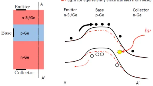
II.5.2.3 Bipolar phototransistors ... 23
II.5.2.4 JFET-based phototransistor ... 24
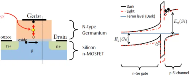
II.5.2.5 Photo-MOSFET photoreceivers ... 25
II.6 Photovoltaic energy ... 26
II.6.1 Why thin-film solar cells ... 27
II.6.2 Basic operating mechanisms of thin-film based solar cells ... 28
Chapter I: Introduction and Thesis Outlines
x
II.6.3 Kesterite-based thin-film solar cells ... 30
II.6.4 Recent progress of kesterite-based solar cells ... 31
II.6.5 CZTS solar cell deposition methods and record efficiencies ... 31
II.7 Conclusion ... 34
III.1 Introduction ... 36
III.2 Global optimization and heuristic algorithms ... 36
III.3 What is metaheuristic techniques? ... 37
III.4 Classification of metaheuristic techniques ... 38
III.5 Genetic Algorithms (GA) ... 39
III.6 Multiobjective optimization ... 43
III.7 Particle swarm optimization (PSO) ... 44
III.7.1 Strength and weakness of the PSO-based approach ... 47
III.8 Quantum Particle swarm Optimization (PSO) ... 48
III.9 Potential application of PSO and GA techniques to boost up the performance of various optoelectronic devices... 50
III.11 Conclusion ... 51
IV.1 Introduction ... 53
IV.2 Part (1): Role of Optimized Grooves Surface-Textured Front Glass in Improving TiO2 Thin Film UV Photodetector Performance ... 54
IV.2.1 Motivation ... 54
IV.2.2 Modeling framework ... 55
IV.2.2.1 Analytical model of the photocurrent ... 57
IV.2.3 Results and discussions ... 59
IV.2.2.1 Optical parameters (FoMs) analysis ... 61
IV.2.2.2 Optimization of MSM-TiO2 UV photodetector performance ... 63
IV.3 Part (2): A Novel High-Performance Self-Powered Ultraviolet Photodetector: Concept, Analytical Modeling and Analysis ... 67
IV.3.1 Motivation ... 67
IV.3.2 Analytical modeling methodology ... 68
IV.3.3 Results and discussions ... 71
IV.3.4 Optimization of the proposed self-powered photodetector design... 76
IV.4 Conclusion ... 80
Chapter III:
Metaheuristic Techniques
xi
V.1 Introduction ... 83
V.2 Part (1): Planar Junctionless Phototransistor: A Potential High-Performance and Low-Cost Device for Optical-Communications ... 84
V.2.1 Motivation ... 84
V.2.2 Modeling methodology ... 85
V.2.3 Results and discussions ... 91
V.2.4 Device performance optimization ... 96
V.3 Part (2): Boosting the Optical Performance and Commutation Speed of Phototransistor Using SiGe/Si/Ge Tunneling Structure ... 98
V.3.1 Motivation ... 98
V.3.2 Device structure and simulation ... 99
V.3.3 Results and discussions ... 103
V.4 Conclusion ... 110
VI.1 Introduction ... 113
VI.2 Part (1): Graded Band-Gap Engineering For Increased Efficiency in CZTS Solar Cells ... 114
VI.2.1 Motivation ... 114
VI.2.2 Analytical modeling methodology ... 115
VI.2.3 Results and discussions ... 121
VI.2.4 The hybrid approach used for improving the conversion efficiency ... 123
VI.3 Part (2): Role of Intermediate Metallic Sub-Layers in Improving the Efficiency of Kesterite Solar Cells: Concept and Optimization ... 127
VI.3.1 Motivation ... 127
VI.3.2 Solar cell designing methodology ... 128
VI.3.3 Results and discussions ... 129
VI.3.4 The proposed design methodology exploited for boosting the conversion efficiency ... 133
VI.4 Conclusion ... 139
VII.1 Introduction ... 142
VII.2 Experimental detail ... 143
Chapter VI: Boosting up the Efficiency of Thin-Film CZTS
Solar Cells
Chapter VII: An Experimental Investigation of a New Au/ITO/Si
Schottky Barrier Diode Design
Chapter V: Design and Optimization of Novel Ge-based
Phototransistor Designs
xii
VII.2.1 RF sputtering technique ... 145
VII.3
Results and discussion ... 148
VII.4 Conclusion ... 157
VIII.2 High-performance Photodetectors with Reduced Power Consumption ... 160
VIII.3 Bridging the Gap Between Nanoelectronic and Silicon Photonics Technologies .... ... 161
VIII.4 Boosting the Conversion Efficiency of CZTS Solar Cells ... 162
VIII.5 Improving Au/Si SBD Electrical and Thermal Reliability Performances ... 163
VIII.6 Outlooks ... 163
REFERENCES ... 166
xiii
List of Figures
Figure II.1. Communication systems versus the length of the interconnection. ... 13
Figure II.2. Conventional optical interconnects receiver circuit. ... 15
Figure II.3. Structure and band-diagram of the MSM photodetector... 16
Figure II.4. A technology roadmap leading to next generational chip-scale photodetectors ... 17
Figure II.5. (a) Schematic of UV-photodetector based on ZnO-NWs/Go/Si hybrid structure, (b) I-V characteristics of the device under dark and illumination conditions. ... 18
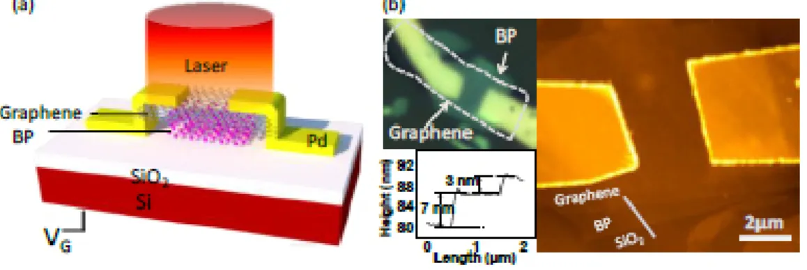
Figure II.6. (a) Schematic illustration of the graphene-BP photodetector. (b) Morphology of the graphene-BP heterostructured device: optical microscopy photograph. ... 19
Figure II.7.(a) Schematic of the ZnO-based self-powered photodetector, (b) UV photodetectors based on n-ZnO/p-NiO core-shell heterojunctions responsivity. ... 20
Figure II.8. High improvement of the performance of ZnO nanowire photodetectors by Au nanoparticles. ... 21
Figure II.9. BP-phototransistor schematic and band diagram with and without illumination ... 24
Figure II.10. Photo-JFET schematic and band diagram of a cross section of the device with and without illumination. ... 24
Figure II.11. Photo-MOSFET schematic and band diagram of a cross section of the device with and without illumination. ... 25
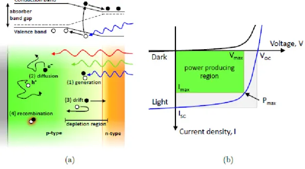
Figure II.12. (a) Illustration of the main charge carrier processes in a conventional p-n junction solar cell, (b) I-V characteristics of a p-n junction diode under both dark and illuminated conditions. ... 29
Figure II.13. Conventional CZTS-based solar cell architecture. ... 30
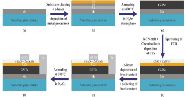
Figure II.14. Schematic representation of the general elaboration steps followed for the fabrication of the CZTS-based solar cell. ... 32
Figure II.15. Top-view and cross-sectional view SEM images of the CZTSSe-based solar cell device with 12.6% record efficiency. ... 33
Figure III.1. Flow diagram of genetic algorithm. ... 40
Figure III.2. Two-point crossover operator. ... 42
Figure III.3. Mutation Operator. ... 42
Figure III.4. (a) MO optimization using weighted sum approach. (b) Pareto front optimality ... 44
Figure III.5. The Standard flowchart of the PSO-based approach. ... 46
xiv
Figure IV.1. Cross-sectional view of (a) conventional TiO2 based UV photodetector, (b)
proposed UV photodetector with grooves. ... 55 Figure IV.2. (a) Absorbance versus the free space wavelength for both planar and back textured structures.(b)Electric field profile for both planar and periodic back textured structures for two different wavelength, with d=200 nm, W=100nm, h = 100nm. ... 59 Figure IV.3. I-V characteristics of the proposed design with grooves compared with that of the conventional planar design with and without illumination. ... 60 Figure IV.4. Device responsivity against the free space wavelength for both planar and back textured structures ... 62 Figure IV.5. (a) Absorbance as function of the free space wavelength for the optimized TiO2 UV-Photodetector with grooves morphology, (b) Electric field profile for the
optimized TiO2 UV-Photodetector with back texturization structure. ... 64
Figure IV.6. I-V characteristics of the optimized design with grooves compared to both conventional planar design and the proposed design without optimization... 67 Figure IV.7. (a) Cross-sectional view of the investigated MSM-based DM-UV-PDs, (b)
equivalent circuit representation of the photocurrent modeling... 69 Figure IV.8. I-V characteristics of both the proposed ZnO/ZnTe MSM-based
DM-UV-PDs design and the experimental results of MSM-UV-PD based on TiO2 nanorod
structure with and without illumination. ... 72 Figure IV.9. I-V characteristic of the conventional design compared with that of both proposed designs based on ZnO/ZnTe and ZnO/TiO2 lateral heterojunctions under
illumination. ... 73 Figure IV.10. (a) Device detectivity and sensitivity against the normalized spacing length position for the proposed ZnO/ZnTe MSM-based DM-UV-PDs. (b) Variation of the Device responsivity and SN ratio against the normalized first region length. . 74 Figure IV.11. Flowchart of the proposed PSO-based optimization approach. ... 77 Figure IV.12. Evolution of the normalized overall objective functions versus the number of generation. ... 78 Figure V.1. Cross-sectional view of the proposed JL-OCFET phototransistor. ... 86 Figure V.2. I-V characteristics of the proposed JL-OCFET for different optical powers .. .
... 92 Figure V.3. Variation of the ION/IOFF ratio against the Ge-gate doping concentration of
the proposed JL-OCFET design for dissimilar applied gate voltage compared with that of the conventional IM-OCFET. ... 93 Figure V.4. Device detectivity versus the applied optical powers for different designs (conventional IM-OCFET, proposed JL-OCFET) ... 94 Figure V.5. Variation of the device sensitivity and the signal-to-noise ratio as function of the applied gate voltage. ... 95
xv
Figure V.6. Cross-sectional view of the investigated OC-TFET with SiGe/Si/Ge hetero-channel aspect. ... 99 Figure V.7. (a) I-Pi characteristics of the proposed Ge-based OC-TFET with different
hetero-channel configurations with Nch=1017 cm−3, Ns=5×1019cm−3, xGe=50%, fixed
gate voltage Vgs = 0.4 V and drain voltage Vds = 1 V. (b) comparison of Band
diagrams associated with the proposed OC-TFET design with uniform Si channel for different applied optical power intensities. ... 104 Figure V.8. Variation of the optical swing factor and the ION/IOFF ratio against the SiGe
source Ge mole fraction for the investigated SiGe/Si/Ge-based OC-TFET structure. .. ... 107 Figure V.9. Device detectivity versus the applied optical power for the proposed SiGe/Si/Ge-based OC-TFET compared to that of the conventional designs based on IM and JL technologies. ... 108 Figure V.10. Variation of the device sensitivity and responsivity as function of the channel thickness... 109 Figure VI.1. (a) Cross-sectional view of the proposed CZTS-based solar cell with
graded band-bap aspect, (b) graded band-gap profile in the CZTS absorber layer. 115 Figure VI.2. I-V characteristics comparison between the experimental data and the developed model of the conventional CZTS-based solar cell ... 121 Figure VI.3. I-V curves of the conventional CZTS-based solar cell compared to that of the proposed design including the graded band-gap paradigm. ... 121 Figure VI.4. The conversion efficiency and the open circuit voltage as a function of the CZTS absorber layer thickness for both proposed and conventional CZTS-based solar cell ... 122 Figure VI.5. I-V characteristics of the optimized design compared to that of both the proposed design with a random band-gap profile and the conventional solar cell counterparts. ... 125 Figure VI.6. EQE curves associated with the conventional design compared to that of
the optimized CZTS-based solar cell with. ... 126 Figure VI.7. Cross-sectional view of the proposed CZTS-based solar cell with intermediate metallic sub-layers... 128 Figure VI.8. Absorbance and reflectance versus the free space wavelength for the conventional design compared to the proposed designs including metallic sub-layer (Ti, Au and Ag) ... ... 130 Figure VI.9. I-V curves of the conventional CZTS solar cell compared to that of the proposed designs including with dissimilar metallic sub-layer (Ti, Au and Ag). .... 131
xvi
Figure VI.10. The conversion efficiency as a function of the metallic sub-layer position for the proposed structures including different metallic sub-layers (Ti, Au and Ag). ... 132 Figure VI.11. Flowchart of the proposed PSO-based optimization approach. ... 134 Figure VI.12. (a) Absorbance versus the free space wavelength for conventional design and the optimized structures with intermediate metallic sub-layers aspect. (b) Electric field distribution associated with both the conventional CZTS solar cell and the optimized design with Ti intermediate metallic thin-films. ... 136 Figure VI.13. I-V characteristics of the optimized design with Ti ultrathin metal layers compared to that of both the proposed design with a random geometrical configuration and the conventional CZTS solar cell counterparts. ... 137 Figure VII.1. (a) Cross-sectional view of the investigated Au/Si SBD with ITO intermediate thin layer. (b) The camera image of the elaborated Au/ITO/Si/Au structure. ... 144 Figure VII.2. The basic working mechanism associated with the RF sputtering technique. ... 146 Figure VII.3. The RF sputtering MiniLab 060. ... 147 Figure VII.4. The semi-logarithmic current-voltage (I-V) characteristics associated with the conventional Au/Si SBD design and the proposed Au/ITO/Si/Au structures with different ITO thicknesses at room temperature. ... 148 Figure VII.5. (a) Variation of the investigated structure Au/ITO/Si/Au ideality factor and Schottky barrier height as a function of the intermediate ITO layer thickness. (b) Series resistance and interfacial density of states versus the introduced ITO thin-film thickness. ... 151 Figure VII.6. The energy distribution profiles of interface density of states for both conventional and proposed designs. ... 153 Figure VII.7. Temperature dependence of (a) ideality factor and Schottky barrier height, (b) interfacial density of states and saturation current, (c) Series resistance associated with the proposed Au/ITO/Si/Au structure and the conventional Au/Si SBD design with tITO=5nm. ... 155
Figure VII.8. I-V characteristics associated with the conventional Au/Si SBD design and the proposed Au/ITO/Si/Au structure including thermal annealing at T=400°C in the temperature range of 20°C-80°C with tITO=5nm. ... 156
xvii
List of Tables
Table II.1. Selection of top record efficiencies for CZTS based solar cell. ... 33 Table IV.1. Comparison of optical and electrical performance obtained from our
optimized device with back texturization with that of the conventional (planar) structure for UV optical communication applications. ... 66 Table IV.2. Overall performance metrics comparison obtained from the optimized MSM-based DM-UV-PDs designs with that of the experimental results of ZnO-based self-powered design for optical communication applications ... 80 Table V.1. Overall performance metrics comparison obtained from our optimized
JL-OCFET device with that of the conventional IM-JL-OCFET for optical communication applications... 98 Table V.2. Device design parameters used in our simulation... 101 Table V.3. Overall electrical and optical FoMs comparison between the proposed SiGe/Si/Ge-based Ge-OC-TFET and both conventional designs with IM and JL technologies. ... 110 Table VI.1. Overall performance metrics obtained from the proposed design with and without optimization compared with that of the experimental results of the conventional CdS/CZTS-based solar cell. ... 126 Table VI.2. Overall performance metrics obtained from the optimized designs with dissimilar metallic sub-layers (Ti, Au and Ag) compared with that of the experimental results of the conventional CdS/CZTS-based solar cell ... 138
xviii
List of Publications
The work in this thesis was mainly drawn from the following publications:
• H. Ferhati, F. Djeffal, “Role of Optimized Grooves Surface -Textured Front Glass in improving TiO2 Thin Film UV Photodetector Performance,” IEEE sensors
journal, vol. 16, pp. 5618- 5624, 2016.
• H. Ferhati, F. Djeffal, “A novel high-performance self-powered ultraviolet photodetector: Concept, analytical modeling and analysis,” Superlattices and Microstructures, vol. 112, pp.480-492, 2017.
• H. Ferhati, F. Djeffal, “Planar junctionless phototransistor: A potential high-performance and low-cost device for optical-communications,” Optics & Laser Technology, vol.97, pp.29-35, 2017.
• H. Ferhati, F. Djeffal, “Boosting the optical performance and commutation speed of phototransistor using SiGe/Si/Ge tunneling structure,” Materials Research Express, vol.5, pp. 065902, 2018.
• H. Ferhati and F. Djeffal, “Graded band-gap engineering for increased efficiency in CZTS solar cells,” Optical materials, vol.76, pp. 393-399, 2018.
• H. Ferhati, F. Djeffal, “Role of intermediate metallic sub-layers in improving the efficiency of kesterite solar cells: concept and optimization,” Materials Research Express, vol.5, pp. 036417, 2018.
• A. Benhaya, F. Djeffal, K. Kacha, H. Ferhati and A. Bendjerad, “Role of ITO ultra-thin layer in improving electrical performance and thermal reliability of Au/ITO/Si/Au structure: An experimental investigation,” Superlattices and Microstructures, vol.120, pp. 419-426, 2018.
Chapter I
Introduction and Thesis
Outlines
Abstract: This chapter is focused on presenting the underlying theme of this thesis, which is to address several optoelectronic devices, from a joint theory, modeling and global optimization standpoint. This chapter provides also the main motivation behind investigating several optoelectronic devices. Moreover, we present the photodetector and phototransistor challenges in current optical communication systems. On the other hand, this chapter presents the most pronounced problems associated with the CZTS thin-film solar cells. The proposed approaches and our contributions in this thesis are detailed. This chapter can be considered as an introductory platform of our work, where the thesis outlines are presented.
1
I Introduction
Over the last few years, semiconductor-based devices have become an essential part of our daily life. In fact, the widespread proliferation of information exchange using the internet makes us immersed in a wider diversity of electronic services. Optoelectronic devices constitute an important part of electronic systems and could belong to our home appliances such as the mobile phone, cars, TV, computers or even carbon-neutral energy sources using photovoltaic systems. The main idea behind these devices resides on the interaction between photons and electrons, where materials with strong absorption/emission properties are suitable for optoelectronic applications. In this context, with the recent progress in optical technology, optoelectronic devices are expected to be exploited for chip-level communication applications [1]. In other words, the deficiencies associated with electrical wire links prevent achieving faster inter-chip communication and reduced power consumption [1-3]. For these reasons, optical links have begun to invade on areas that were once considered to be the exclusive dominion of electrical links [4-7]. Modern versions of optical communication have been well-developed thanks to the early progress regarding advanced photoreceivers (photodetectors, phototransistors and photodiodes) fabrication technologies and also to new radical ideas [5-7].
Optoelectronic devices were also emerged for different sensing applications such as: photovoltaic and environmental monitoring systems. Ultraviolet sensors analyze our environment, i.e. they detect the presence UV-radiations in our atmosphere [6-8]. The UV-photodetector as an optoelectronic device is considered of crucial importance for the control of our physical environment [8]. On the other hand, solar cell-based devices are forecasted to be the most strategically desirable solution for recording low cost and clean renewable energy resources [9]. As a matter of fact, the development of high-efficiency solar cells with low-cost to end the actual carbon economy is of fundamental significance in both economics and industrial sectors [10-13]. The main objective is therefore to make a good trade-off between both the elaboration cost and the conversion efficiency, which is unfortunately foreseen as a barrier for achieving low cost carbon neutral energy sources. To this extent, Chalcogenide-based solar cells are expected to be effective for providing an improved efficiency at low manufacturing cost [14]. However, practical challenges, such as structure complexity, efficiency losses and reliability, should also be taken into account [14-18].
2
I.1 Motivation
The continuous demand for low cost optoelectronic devices with high-performance is growing rapidly for diverse electronic applications such as optical communication, environmental monitoring, sensing and even photovoltaic energy. In this framework, the development of high-performance optoelectronic devices like phototransistors, photodetector and high efficiency solar cells is of paramount importance in nowadays industry requirement. In this regard, we have conducted a variety of studies to propose and develop novel design methodologies to address the most critical challenges associated with the current optoelectronic devices. Therefore, the enhancement of these devices seems of great importance which motivates us for investigating several optoelectronic devices including UV-photodetectors and NIR-phototransistors and thin-film solar cells in order to deal with the most pronounced issues faced by these devices.
I.2 The Gap Between Electronic and Photonic
The integration between photonics and electronics could improve CMOS capabilities and open up a new way toward continuing feature size shrinkage according to Moore’s law. Following this direction, in chip-to-chip communication, shrinking the electrical wire interconnects size imposes several challenges mainly related to the increase in the resistivity, the total capacitance and power consumption, which results in an enormous reduction of the communication bandwidth [2-5]. Alternatively, integrated silicon photonics provide great promise in meeting the high bandwidth and low-energy demands since they offer the opportunity of optical communication technology [3-6]. In fact, optical interconnection technology offers the distance insensitivity property owing to the inherently low optical losses of fibers, enabling the prospect for new types of communications in modern digital systems and data-transfer centers. Three years ago, the first single-chip computer in which the connectivity was down by means of optical links based on monolithic integrated photonic technology is successfully demonstrated [5]. In spite of this achievement, there are still many challenges associated with silicon photonic interconnect that prevent the deployment of the optical links for the current nanoelectronic technology. As the industry moves towards the optical communications, their three essential stages namely, emitters, transmitters and photoreceivers should be improved in order to make the electronic-photonic integration very close. Therefore, it has become important to propose new insights in order the make the optical
3 communication technology more competitive with the electrical counterparts and to potentially improve the communication bandwidth.
I.3 Cost and Power Challenges
Power consumption is considered as the most pronounced problem of today's chip designers. Although the continuous downscaling has allowed a considerable increase in number of transistors and memory bits per chip, the power dissipation drawbacks prevent achieving high-performance designs at the upcoming technology nodes. Over the last few years, the recent progress regarding the optical wireless communication technology in chip-level communication has provided a new path toward achieving lower resistive losses and an enormous bandwidth [4-5]. However, this system consumes a huge amount of power due to the high energy dissipation of the photoreceiver circuit. In this perspective, the optical links technology faces the challenge of how to translate the photoreceiver devices into better performance under reduced power consumption. Moreover, the photoreceiver should be followed by Trans-Impedance Amplifier (TIA), to remove noise that gives digital transmission its high quality levels for optical communications systems. Moreover, amplifier stages are also used to convert the photoreceiver current to voltage signals that can be accepted by CMOS logic stages. These readout circuits consume a huge amount of power. In order to deal with this problem the optical receiver output capacitance should be minimized. On the other hand, several photoreceiver devices are exploited to develop the optical communication including photodetectors, photodiodes and phototransistors. The manufacturing cost of these structures is also considered a big issue, where it is of great importance to improve the photoreceiver performance with keeping the low cost property. Moreover, enhancing the optical receiver sensitivity, responsivity and optical commutation speed can be effective for reducing the light power intensity from the emitter which could decrease the overall energy consumption of the optical wireless communication systems. As a result, the second goal of this thesis is to get rid of power consumption issues and decrease the elaboration cost of the photoreceiver stage. Specifically, we will focus on improving the photodetectors and phototransistors performance and potentially suppressing leakage power.
4
I.4 CZTS (Cu
2ZnSn(S,Se)
4) Thin-Film Solar Cell Challenges
Several challenges still prohibit the implementation of CZTS-based technology as a compelling solution for achieving high-efficiency and low-cost photovoltaic device. In fact, the maximum achievable efficiency value associated with the Kesterite-based solar cell is reported to be approximately 30% [19]. Unfortunately, to date only 12.6% of conversion efficiency was recorded, which is considered very low and required further enhancement [20]. It is of great importance to understand the main reasons that prevent approaching the theoretical limit of the CZTS based solar cell. Accordingly, there are some problems regarding the solar cell design and the material quality and even experimental issues that can affect the device performance. Therefore, there are five essential effects that should be addressed in order to improve the solar cell performance: Voc deficit: although an acceptable Voc value about 0.7 V has been recently recorded [20], the open circuit voltage values are generally reported to be at the average of 550 mV. This indicates that there is a great deficit when compared to the theoretical limit of 1.23 V forecasted for CZTS-based thin-film photovoltaic technology. The Voc deficit associated with the actual Kesterite solar cells can be attributed to two main factors namely the quality of the absorber layer and the degradation related-recombination effects.
Low diffusion length: with minority carrier lifetime about 2.5ns, the CZTS compounds are considered extremely challenging for achieving superior values of the open circuit voltage. In this context, charge carrier transport parameters should be considerably improved. To do so, the good control of the CZTS compositional homogeneity as well as the phase purity can give wider possibilities for extending the carrier diffusion length and thereby enhancing the solar cell performance.
Intrinsic defects and stability issues: the quality of the absorber layer CZTS plays a crucial role in determining the solar cell performance, where intrinsic defects can enormously degrade the device efficiency. Indeed, these defects can cause the electron-hole pair recombination phenomena, which are considered as major challenges that prohibit achieving favorable efficiency values. These effects are mainly due to the experimental conditions (fabrication processes) as well as the elaborated CZTS compositions. Therefore, the complexity associated
5 with different growth techniques and elaboration conditions constitute a major drawback for the better understanding of these experimental problems.
CZTS solar cell design: engineering the device architecture appropriately can be beneficial for improving the conversion efficiency. The optimization of the absorber layer and the good choice of the buffer layer and contacts can offer the possibility to further increase the device efficiency. In fact, the actual Kesterite-based solar cell exhibits extensive limitations related to non-ohmic behavior of the back contact due to the formation of a potential barrier between the CZTS active region and the MoS2 interfacial layer. This phenomenon can affect the device performance and causes significant degradation on the short-circuit current.
CZTS/Buffer layer interface quality: the standard solar cell design adopted for CIGS is typically used for the CZTS-based photovoltaic device counterpart, where the material used as buffer layer is the CdS. This material has shown a good compatibility and improved interface quality for the CIGS technology, which is not the case for the Kesterite solar cells. In fact, the biggest problem is the band-alignment between CdS and CZTS, where the interfacial defects at the interface induces recombination losses. Moreover, the use of the CZTSSe absorber layer can give rise to possible enhancement regarding the solar cell absorption behavior, but with consequential increase of the interfacial defects. Thus, exploring suitable Cd-free buffer layers is obviously desirable not only from an environmental point of view, but also for improving the Kesterite solar cell performance.
In summary, a deep knowledge of the basic material properties, interfacial defects origin and the solar cell degradation reasons is certainly an important issue to identify both the appropriate buffer layer and the optimal CZTS absorber layer that enable improving the solar cell conversion efficiency. In this perspective, the third objective of the thesis work focuses on investigating the prospect for improving the Kesterite solar cell performance by taking into consideration the above-mentioned critical issues.
I.5 Our Approaches and Contributions
This section presents the approaches we use to bridge the gap between photonics and electronics as well as reducing both the fabrication cost and power consumption of
6 photoreceiver structures including photodetectors and phototransistors. New concepts for the eventual enhancement of the CZTS solar cell efficiency are also provided.
Bridging the Gap Between Electronic and Photonic
Optical components used for the optical interconnections such as modulator, waveguide and (photodetector or phototransistors) should be integrated with advanced CMOS technology. One of the major objectives of the thesis is how to address the size mismatch between current electronic and photonic components, and achieve further promising improvements regarding the photoreceivers performance. For this purpose, we propose versatile Ge-phototransistor designs which are fully compatible with CMOS technology. The first one consists on a new junctionless Ge-phototransistor that provides substantial improvement regarding the device FoMs. The main objective is also to improve the photoreceiver performance and potentially bridge the gap between the advanced electronic technology and its silicon photonic counterpart. This benefit is achieved through using a suitable sensitive material that is effective in the near-infrared wavelength ranges and simultaneously compatible with silicon. In a similar manner, the second proposed Ge-phototransistor design suggests introducing a hetero-channel structure in order to generate the quantum band-to-band tunneling effect. The latter can provide small swing switch property which can enhance the phototransistor optical commutation speed. Moreover, the proposed design is suggested with SOI platform in order to make it potentially compatible with CMOS technology.
Reducing Power Consumptions and Fabrication Costs
It is of great importance to reduce the photoreceiver power consumption. As a matter of fact, suppressing the leakage current of the photodetector and phototransistor could reduce the power dissipation. Moreover, taking lower applied voltages can also enormously decrease the power budget. Following this direction, the aim of this dissertation is to explore new design methodologies for removing the power issues. In this perspective, we propose a new self-powered photodetector that operates at zero bias conditions. A heterojunction channel is suggested to ensure the self-powered property. Moreover, we exploit metaheuristic techniques to achieve high-performance photodetector at zero voltage. Besides, the proposed design is suggested with earth abundant materials in order to reduce the fabrication cost.
7 The second approach is based on combining a new junctionless phototransistor design with metaheuristic techniques to potentially achieve the dual role of improved device performance and reduced power consumption. Moreover, we suggest the phototransistor without junctions at the source/drain regions in order to reduce the fabrication process and to avoid the thermal budget.
The third approach consists of proposing a new phototransistor design based on tunneling effect in order to suppress the leakage current that can subsequently reduce the power consumption. More importantly, using a phototransistor instead of photodetector as a photoreceiver in optical wireless communication systems could provide the receiver-less property that allows avoiding the use of amplification stages and thereby a considerable decrease in both energy consumption and cost challenges.
Overcoming the CZTS Solar Cell Critical Challenges
The CZTS thin-film has drawn world-wide attention due to its outstanding photovoltaic performance and earth-abundant composition. However, nowadays CZTS-based solar cells efficiency values are still far from its theoretical limit. This is because of several limitations mainly associated with degradation-related recombination effects, optical losses and elaboration issues, which are above outlined. Thus, improved efficiency values are envisaged in order to make the CZTS solar cell technology competitive with its counterpart based on silicon. Accordingly, we focus our efforts on developing new approaches that enable improving the CZTS solar cell conversion efficiency. After the careful study of the CZTS-based solar cell working mechanisms, we have obtained three key insights that allows improving the solar cell performance
Avoiding the degradation related-recombination effects The substantial reduce in the optical losses
The series resistance modulation
These insights indicate that we can design the CZTS solar cell in an appropriate way that enables reaching these objectives. For this reason, we firstly propose a new design based on graded band-gap aspect to effectively suppress the recombination effects and hence improve the solar cell efficiency. The main idea behind it is to generate an electric field in the CZTS absorber layer that could efficiently derive the photogenerated carrier. We also use a metaheuristic technique to identify the favorable CZTS band-gap profile that provides the maximum possible efficiency value. The optimized design could open up the route not only for improving the minority carrier
8 life time but also for enhancing the absorbance behavior that can in turn offer superior efficiency values. The proposed CZTS solar cell design takes advantage from the electric field modulation aspect to provide the possibility to reduce the series resistance. Secondly, the CZTS solar cells have certain weakness mainly related to the high series resistance originated from the formation of the MoS2 at the CZTS/Mo interface. The optical losses constitute also a serious problem that we should deal with. For this purpose, we propose a new design methodology based on coupling global optimization approach with a new solar cell structure with intermediate metallic layers. The latter are introduced in the CZTS absorber layer in order to achieve the dual benefit of preventing the sulfide diffusion and enhancing the absorption near the infrared spectrum range. We use various metallic sub-layers in order to identify the most favorable metal that provides the highest efficiency value. As a result, substantial improvements regarding the solar cell fill factor and photocurrent can be achieved by appropriately avoiding antireflection effects.
I.6 Thesis Outlines
The underlying theme of this thesis is to address several optoelectronic devices, from a joint theory, modeling and global optimization standpoints, with a focus on understanding the physical rules that governs their optical and electrical performances. This work is motivated in a part by the photodetector and phototransistor challenges in current optical communication systems and in another part by the search for new approaches to achieve improved conversion efficiency for the CZTS thin-film solar cells. The rest of this thesis is organized as follows:
The second chapter presents an overview of fundamental concepts concerning several optoelectronic devices. At the beginning, we define the conventional photoreceiver devices such as photodetectors and phototransistors, and we give a detailed description of their recent progress and future challenges. Then we define and describe the CZTS thin-film solar cells and their basic operating mechanisms. A detailed literature review on the CZTS solar cell deposition methods and record efficiencies is presented.
General concepts and description of metaheuristic techniques are presented in Chapter III. This chapter introduces the fundamentals of genetic algorithm (GA),
9 Particle Swarm Optimization (PSO) and its quantum derivative termed (QPSO). An overview of multi-objective optimization approaches in also presented.
In Chapter IV, we consider the enhancement of UV photodetectors (PD). In the first part, the impact of the surface-textured front glass on the absorption of TiO2/glass Metal-Semiconductor-Metal (MSM) UV photodetector is investigated, in order to achieve the dual role of increasing the scattering path as well as reducing the refracting UV-light at the glass substrate. Moreover, semi-analytical modeling combined with PSO-based approach is carried out for studying and enhancing the MSM-UV photodetector optical and electrical performances. The second part of this chapter is devoted to the investigation of a new self-powered MSM-UV-photodetector based on dual wide band-gap material (DM) engineering aspect. Comprehensive analytical models for the proposed sensor photocurrent and the device properties are developed incorporating the impact of DM paradigm on the device photoelectrical behavior. A new hybrid approach based on analytical modeling and PSO approach is proposed to achieve improved photoelectric behavior at zero bias that can ensure favorable self-powered device.
Chapter V of this thesis investigates the prospect for improving the Ge-phototransistor performance by proposing two novel structures. The first one consists of a new junctionless optical controlled field effect transistor (JL-OCFET), where its comprehensive theoretical model is developed. The latter is exploited to formulate the objective functions to optimize the device performance using GAs. The optimized design offers high optical performance and low cost fabrication process. On the other hand, a new optically controlled tunneling field effect transistor (OC-TFET) based on SiGe/Si/Ge Hetero-channel is proposed to improve the optical commutation speed and reduce the power consumption. Importantly, a new FoM parameter called optical swing factor that describes the phototransistor commutation speed is proposed.
Chapter VI focuses on providing new insights for the potential improvement of the CZTS-solar cell conversion efficiency. The first idea relies on proposing a potential high efficiency design based on graded band-gap aspect that can offer the benefits of improved absorption behavior and reduced recombination effects. Analytical models for the proposed design are developed incorporating the impact of the graded band-gap profile on the solar cell photoelectrical behavior. A new design methodology based on
10 analytical modeling and PSO approach is proposed to determinate the better band-gap shape of the amended CZTS absorber layer. The second idea consists of investigating the role of intermediate metallic sub-layers (Au, Ti, and Ag) engineering coupled with metaheuristic techniques in enhancing light-scattering behavior and reducing recombination losses.
Finally, the last Chapter of this thesis explores the concept of using a new Au/p-Si SBD based on ITO intermediate thin-film to improve the diode electrical behavior. The device performances are experimentally investigated. The effect of the annealing temperature on the SBD electrical performance is also investigated. In order to show the role of the inserted ITO layer thickness on the device performance, we elaborated Au/ITO/p-Si structures with different ITO thicknesses by means of RF magnetron sputtering technique. The role of the annealing process in improving the SBD basic electrical parameters and thermal stability performance is also discussed. Finally, an overall performance comparison between the fabricated SBD structures with and without intermediate ITO layer is carried out.
11
Chapter II
Optoelectronic Devices:
Concept and Recent Progress
Abstract: This chapter presents an overview of fundamental concepts associated with several optoelectronic devices. At the beginning, we define the conventional photoreceiver devices such as photodetectors and phototransistors, and we give their basic working principle. We thereafter provide a detailed description of their recent progress and future challenges. Then we describe and elucidate the main challenges of the CZTS thin-film solar cells and their basic operating mechanisms. A detailed literature review concerning the CZTS solar cell deposition methods and record efficiencies is finally presented.
12
II.1. Chapter overview
Optoelectronic devices have been aggressively driven into several domains of application such as: optical communication, environmental monitoring and clean-renewable energy. In this work, we are mostly interested in optical photoreceivers (photodetectors and phototransistor) and photovoltaic devices based on CZTS material. In this chapter, we will briefly discuss the operating mechanisms associated with several optoelectronic devices. To beginning, we defining different photoreceiver devices, and we will give a global description of their potential applications. Then we will describe the CZTS-based solar cells technology and their advantages in comparison with other photovoltaic devices. The future challenges for developing high-efficiency solar cells are also presented. This chapter can be considered as an introductory platform for upcoming chapters.
II.2. Electrical interconnect
Eelectrical wiring has been considered as an efficient means of communication at various levels of electronic systems, and currently they still dominate the chip-to-chip and broad-to-broad interconnections. Microelectronic systems have offered a steady downscaling in accordance with Moore’s law, which is the key towards achieving denser circuitry with high-performance chip and reduced power consumption [21]. Despite the fact that the continuous shrinking of transistors dimension is expected to eventually enhance chips performance, the Semiconductor Industry Association (SIA) has claimed that extensive limitations will be appeared in the future, which could prevent the good operating of the overall chip system [1], [21-22]. These concerns are mainly associated with metallic wires that connect chips to each other [2]. In this context, this problem is considered as one of the major issues in the future progress of integrated microelectronic circuits. The downscaling of the electrical wire increases the resistivity and thereby enlarges the total power consumption of the link, which degrades enormously the communication bandwidth. In order to avoid these problems, complicated signal processing techniques can be used to improve the information capacity, but in contrast, this can certainly further increase the overall cost of the communication system. For these reasons, alternative approaches should be developed in order to cope with the growing demand for larger communication bandwidth at chip level scale.
13
II.3. Optical interconnect as an alternative technique
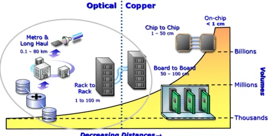
Light is considered as electromagnetic (EM) waves for which the wavelengths are extended from Ultra-violet to Infrared range, where their ability to propagate at a very high-speed and for long distances constitute their main advantage. Indeed, optical communications came of age after the prestigious invention of the laser and photodetectors, which are an application of Einstein’s theories in which a photon could stimulate an excited atom to emit another identical photon as well as the photoelectric effect that describes the UV-light detection phenomenon. Optical interconnects have been proposed as one of the promising candidates to replace traditional electrical wires due to their potential for overcoming the most pronounced challenges associated with the electrical links including the communication bandwidth [3-5]. The use of optical fibers or waveguides provides the opportunity for getting rid of the undesired resistive losses exhibited by the electrical wire. The deployment of interconnection systems with respect to the communication distance is presented in Figure II.1. Optical links technology not only dominates the long haul communications, but also it consistently pinpoints the way toward governing shorter distances. Meanwhile, till now inter chips and board connections are still done electrically [4-6].
Figure II.1: Communication systems versus the length of the interconnection.
The major problem associated with the electrical connections technology is the huge overhead in energy consumption [6]. On the other hand, alternative approaches such as optical links should demonstrate reduced energy consumption. However,
14 although the large bandwidth offered by optical communication, transmitters and receivers typically, consume a considerable quantity of power, which makes the optical interconnects extremely challenging at short distance communication applications.
II.4. Optical interconnect challenges
There are many challenges for optical communication that should be addressed in order to make them competitive with electrical interconnections. In this context, typical optical interconnects require high-speed and low power electronics as well as optical components [5-6], [23]. Thus, the most pronounced problems for the optical links to become more efficient are described below.
Power consumption: It is even desirable to run the receiving end of the link without amplification stages. In a traditional optical receiver, the optical signal is conveyed by an emitter through the waveguide to the receiving-end of the optical interconnects. Then, the optical signal will be converted into an electrical current by means of photodetectors. Finally, transimpedance amplifiers is used to convert current to an electrical voltage, which will be amplified using subsequent electronic circuitry to reach the logic level as it is illustrated in Figure II.2. This configuration can consume a huge amount of power, which constitutes a serious problem for the deployment of the optical links. Moreover, the high density of the receiver circuit can also prevent the use of the optical communication at short distance communication. Therefore, the main objective is to operate the photodetector “receiverless” i.e. avoiding all amplifications in the receiver readout circuit. In addition, to reduce the global power consumption of the optical links, it is important to reduce the light intensity at the emitter stage able to provide a tunable response. In summary, to eventually replace shorter electrical interconnects with the optical ones, the light source should be more efficient, and the optical receiver should be more sensitive.
Monolithic integration: The VLSI technology (Very large scale integration) is considered as the mainstream for the actual microelectronics industry. This mature process is widely used to elaborate the widespread integrated circuit (IC), which is the result of investment and research over a number of decades. Admittedly, optical components associated with the optical links such as modulator, waveguide and the photodetector should be integrated
![Figure II.4: A technology roadmap leading to next generational chip-scale photodetectors [19]](https://thumb-eu.123doks.com/thumbv2/123doknet/14897072.652018/37.892.248.651.305.633/figure-technology-roadmap-leading-generational-chip-scale-photodetectors.webp)
![Figure II.8: High improvement of the performance of ZnO nanowire photodetectors by Au nanoparticles [44]](https://thumb-eu.123doks.com/thumbv2/123doknet/14897072.652018/41.892.289.598.666.1032/figure-high-improvement-performance-zno-nanowire-photodetectors-nanoparticles.webp)
![Figure II.15. Top-view and cross-sectional view SEM images of the CZTSSe-based solar cell device with 12.6% record efficiency [70]](https://thumb-eu.123doks.com/thumbv2/123doknet/14897072.652018/53.892.129.766.486.738/figure-cross-sectional-images-cztsse-device-record-efficiency.webp)