Cleaning Process Development and Optimization in the
Surface Mount Assembly Line of Power Modules
by
Ishan Mukherjee
B.E. Mechatronics Engineering
Manipal Institute of Technology, Manipal, 2010
the Department of Mechanical Engineering in Partial Fulfillment of the Requirements for the Degree of
MASTER OF ENGINEERING IN MANUFACTURING
at the
MASSACHUSETTS INSTITUTE OF TECHNOLOGY
September 2011
0 2011 Ishan Mukherjee. All rights reserved.
The author grants to MIT permission to reproduce and
to distribute publicly paper and electronics copies of this thesis document in whole or in part in any medium known or hereafter created
MASSACHUSETTS INSTITUTE OF TECHNOLOGY
NOV
0
1 2011
LIBRARIES
ARCHIVES
Signature of Author: ... .... ... ... 6partment of Mechanical EngineeringAugust 16, 2011
C ertified b y : ... .. ... ... Jung Hoon Chun Professor of Mechanical Engineering Thesis Supervisor
C e tii e b : ...
.-. ...---
-- .. .ard7
Certfiedby:David E. Hardt
Ralph E. and Eloise F. Cross Professor of Mechanical Engineering Chairman, Department Committee of Graduate Students Submitted to
Cleaning Process Development and Optimization in the
Surface Mount Assembly Line of Power Modules
by
Ishan Mukherjee
Submitted to the Department of Mechanical Engineering on August 16, 2011 in partial fulfillment of the requirements for the Degree of
Master of Engineering in Manufacturing at the Massachusetts Institute of Technology
Abstract
The cleaning process in the surface mount assembly line of power modules had been found to insufficiently remove solder flux residue from printed circuit board (PCB) assemblies after the process of reflow soldering. This thesis details the development of an optimized cleaning process that effectively removes solder flux residue from PCB assemblies. The first stage of this study involves the experimental validation of root cause of process ineffectiveness. A novel visual inspection based grading scale is developed to quantify the amount of residue present. Using the grading scale optimal process parameters were identified and studied. The study finds that power modules are most effectively cleaned in a saponifier based cleaning solution using ultrasonic agitation. Power modules are completely cleaned when washed in an ultrasonic bath at
60*C for 7 minutes, in a saponifier based cleaning solution that is 5% concentration by volume.
Thesis Advisor: Jung Hoon Chun
Professor of Mechanical Engineering
Acknowledgements
I would like to express my sincere appreciation to cohort members of the Master of Engineering
program at the Massachusetts Institute of Technology and to Vicor Corporation for giving me the opportunity to apply my acquired skills in a state of the art work environment.
I would like to thank my thesis advisor, Prof. Jung Hoon Chun, for his invaluable
guidance and encouragement throughout the project.
I would like to thank Mr. Mohammed Wasef and Mr. Rudy Mutter for their support, mentorship and guidance. They provided us with the opportunity to work on a challenging project and gave us responsibilities that far exceeded expectations.
I am grateful to Prof. David Hardt and Dr. Brian Anthony for their support,
encouragement and invaluable help.
I would like acknowledge the support provided by Mr. Steve Caruso, Ms. Eva
McDermott, Ms. Linda Kenison, Mr. Gaurav Sonone, Mr. Ray Whittier and Mr. Karan Barabde at Vicor Corporation.
I am eternally grateful to Nikith Rajendran and Pranav Jain, working on the project with
them was an unforgettable experience. It was an absolute honor to be part of a team that exceeded expectations and delivered timely results.
Lastly, I would like to convey my heartfelt thanks to my Mother, Father and Brother; without their unconditional encouragement and support nothing would be possible.
Table of Contents
A cknow ledgem ents ... 3
List of Figures... 6
List of Tables... 7
1. Introduction ... 8
1.1 Com pany Background... 8
1.1.1 Product Inform ation and D escription... 9
1.2 Overview of Thesis ... 10
2. O verview of M anufacturing Process... 11
2.1 V I Chip M anufacturing Process Flow ... 11
2.1.1 Surface M ount Technology Process ... 12
2.1.2 Transform er Core Attach... 15
2.1.3 U nderfill... 15
2.1.4 M olding... 16
2.1.5 PCB M arking and D icing... 16
2.1.6 J-lead A ttach ... 16
2.1.7 Final Testing ... 16
2.2 Post-SM T Cleaning ... 17
2.2.1 PCB Cleaning... 17
2.2.2 W hy Cleaning ... 17
2.2.3 Factors Involved in Cleaning... 18
2.2.4 Cleaning M ethods ... 19
2.3 Process Control and Testing... 20
2.3.1 Process Control Tests... 21
2.3.2 Inadequacy of Current Testing M ethodology ... 22
3. Problem Statem ent ... 23
3.1 Problem D escription... 24
3.1.1 Areas of Residue Incidence on PCB ... 26
3.1.2 Effects of Flux Residue... 29
3.2 Factors Involved... 31
3.2.1 A gitation ... 31
3.2.2 Chem ical A ction ... 33
3.2.3 W ash Tim e ... 33
3.2.4 Tem perature ... 34
3.3 Project Objectives ... 34
4. Literature Review ... 36
5. Cleaning Process Development... 39
5.1 Root Cause Hypothesis Validation ... 40
5.1.1 Pre-Wash Test Cycle... 40
5.1.2 Design of Experiments... 40
5.2 Experiment Methodology... 42
5.2.1 Equipment and Test Board used ... 42
5.2.2 Inspection Methodology ... 44
5.2.3 Cleaning Efficiency Metric... 47
5.2.4 Gage R&R Study ... 52
5.3 Cleaning Process Selection and Optimization ... 54
5.3.1 Analysis of Experiment Data... 54
5.3.2 Criteria for Process Selection... 55
5.3.3 Methods to Optimize Cleaning Process... 56
6. Results and Discussions... 57
6.1 Analysis of Hypotheses Validation Experiments... 57
6.1.1 Effect of Agitation on Cleaning Efficiency ... 57
6.1.2 Effect of Cleaning Agent Concentration on Cleaning Efficiency ... 59
6.1.3 Effect of Time of Cleaning Process on Cleaning Efficiency ... 60
6.1.4 Effect of Cleaning Solution Temperature on Cleaning Solution... 61
6.2 Design Factors Affecting Cleaning Efficiency ... 62
6.2.1 Effect of Component Location on Cleaning Efficiency ... 64
6.2.2 Effect of Module Location on Cleaning Efficiency... 65
6.3 Cleaning Process Optimization... 67
6.3.1 Optimal Cleaning Process Selection... 68
6.3.2 Design of Experiment for Process Optimization ... 71
6.3.3 Result of Process Optimization... 73
7. Summary, Recommendation and Future Work ... 76
7.1 Summary of Cleaning Process Selection and Optimization... 76
7.2 R ecom m endation... 77
7.3 Future W ork ... 78
Appendix A: Run Chart of Experiments... 79
Appendix B: Summary of Gage Repeatability and Reproducibility Study (R&R)... 80
Appendix C: Component Footprint Grading Scale... 82
List of Figures
Figure 2-1 Flowchart of VI-Chip manufacturing process... 12
Figure 2-2 Surface mount technology process flow ... 13
Figure 3-1 Process flow chart ... 23
Figure 3-2 Presence of flux residue under a BGA-FET ... 25
Figure 3-3 Presence of flux residue under chip capacitor array ... 25
Figure 3-4 Flux residue around BGA's and on board... 26
Figure 3-5 Diagrammatic description of "standoff' in a MLP-FET... 27
Figure 3-6 Flux reside on bottom surface of MLP-FET ... 28
Figure 3-7 Flux reside on QM OS footprint ... 28
Figure 3-8 Flux reside on chip capacitor array footprint ... 29
Figure 3-9 Flux reside around BGA older balls... 31
Figure 3-10 Illustration of fluid flow beneath MLP-FET ... 32
Figure 3-11 Presence of flux residue due to improper agitation and fluid flow ... 33
Figure 5-1 Hypotheses validation experiment process flow... 40
Figure 5-2 Cole-parm er ultrasonic cleaner ... 42
Figure 5-3 Experiment test board: VI-Chip-TV-36372... 44
Figure 5-4 Inspection process flow chart... 45
Figure 5-5 Inspected components on top and bottom side of power module ... 46
Figure 5-6 1210 Chip capacitor metric pictorial reference ... 50
Figure 5-7 MLP-FET Metric pictorial reference ... 51
Figure 5-8 Gage R&R study control charts with study variation of 6 standard deviations ... 53
Figure 6-1 Comparison of cleaning scores of ultrasonic and soak cleaning in DI water ... 58
Figure 6-2 Comparison of cleaning scores of centrifugal cleaning with Chemical B... 60
Figure 6-3 Comparison of cleaning scores of ultrasonic agitation in DI water ... 61
Figure 6-4 Comparison of cleaning scores of soak cleaning in 7.5% Chemical B... 62
Figure 6-5 Footprint of bottom side 1210 chip capacitor array ... 63
Figure 6-6 Variation of cleaning scores across capacitors in centrifugal water wash ... 64
Figure 6-7 Variation of cleaning scores across modules in centrifugal water wash... 66
Figure 6-8 MLP-FET underside: variation across three agitations techniques in DI water ... 69
Figure 6-9 Chip-capacitor footprint: prewash soak in three chemical solutions for 10 minutes.. 69
Figure 6-10 Comparison of cleaning techniques ... 70
Figure 6-11 Surface plot of cleaning score vs. time and Chemical B concentration... 74
List of Tables
Table 5-1 D OE process param eters ... 41
Table 5-2 Cleaning efficiency metric description... 48
Table 5-3 Example of dootprint observation data-sheet of Board A ... 48
Table 5-4 Example of component underside observation data-sheet of Board B... 48
Table 5-5 1210 Chip capacitor cleaning efficiency metric ... 50
Table 5-6 MLP FET cleaning efficiency metric ... 51
Table 5-7 Gage R&R study results: percentage contribution of variations ... 52
Table 6-1 Aggregate scores of ultrasonic agitation and soaking ... 57
Table 6-2 Mean and standard deviation of module cleaning scores ... 65
Table 6-3 Experiment results of five cleaning techniques... 71
1. Introduction
This thesis is a result of a project carried out by a research team at the electronics power module manufacturing facility of Vicor Corporation. The application of the manufactured power module lies in the fields of computing, data processing, communications and controls; where the demand is for high product efficiency and reliability. The research team comprising of P Jain [1], N. Rajendran [2] and the author developed an efficient process to remove solder flux residue from printed circuit boards (PCB) after the process of reflow soldering. The study comprised of the root cause analysis of process inefficiency, process development & optimization and manufacturing system analysis. In this thesis, the focus is on the selection and optimization of a cleaning process which consistently removes solder flux residue from PCB's, thus eliminating related product failures.
1.1 Company Background
Vicor Corporation headquartered in Andover, MA is a market-leading provider of electronic power system solutions for the highly specialized electronics industry. The company designs and manufactures modular power components which have applications in various fields such as computing, communications, industrial control, industrial testing and medical and defense electronics. The company manufactures three types of products- Bricks, VI-Chips and Picor components. Bricks and VI-Chips are specialized D.C.-D.C. and A.C.-D.C. power convertors
and filters and include power regulators, current multipliers and bus convertors, whereas the Picor range includes high density power conversion circuit components. In this work, however, the focus is on the manufacture and quality improvement of VI-Chips.
1.1.1 Product Information and Description
VI Chip refers to the name given to the latest series of DC-DC converters released by Vicor which have higher power density, higher efficiency, improved transient responsiveness, lower noise levels and lower costs than the previous series of DC-DC converters. DC-DC converters are an integral part of many electronic and electrical applications and are used whenever there is a need to either step-up (also referred to as 'boost') or step-down (also referred to as 'buck') the input voltages in order to deliver an output voltage. A typical example could be observed in a car were different electrical appliances like headlights, radio, etc. require different input voltages and hence would need a DC- DC converter to convert the input voltage from the car battery to meet the different voltage requirements. This DC-DC conversion can be achieved through the VI -chipset which includes different modules like PRM (Pre-Regulator Module), VTM (Voltage Transformer Module), BCM (Bus Converter Module), etc. Evidently, each of these modules has different product architectures. But they can be still produced on the same production line.
The PRM can be predominantly associated with the voltage regulation work i.e. it delivers a highly regulated voltage from an unregulated input source. Though PRM can be used just as a power regulator, it is usually used in conjunction with the VTM which uses the regulated voltage from the PRM and transforms it according to the demand. Thus a PRM - VTM combination essentially serves as a regulated DC - DC converter. BCM module is a supplementary module
which is a fixed DC - DC voltage transformer that can be used along with the regular PRM -VTM combination and usually used to provide intermediate voltages. This modular approach of having three or more different modules (PRM, VTM and BCM) for achieving the function of a
DC - DC converter is result of the 'Factorized Product Architecture (FPA)' philosophy
introduced and followed by Vicor instead of the regular 'Centralized Product Architecture
(CPA)' adopted by the rest of the industry.
1.2 Overview of Thesis
This thesis is a result of collaborative research work carried out by P. Jain [1], N. Rajendran [2] and the author from January through August 2011. The research team set out to first jointly study the manufacturing system and its constituent assemblies. This was followed by an in-depth research in the physics of the cleaning process and of the DI water based cleaning system installed in the facility. In this thesis, Chapter 2 explains these two stages by describing the manufacturing processes and the essential background concepts. Chapter 3 focuses on the formulation of the problem being tackled and sheds light on the specific details of the inefficient cleaning of solder flux residue. Following the problem statement, Chapter 4 presents a brief summary of industrial and academic research carried out in related fields. At this stage the thesis breaks off to elaborate on the individual work done by the author in selecting the best cleaning process and optimizing it. Chapter 5 explains the basis, methodology and testing procedures
while Chapter 6 present experimental results and related discussions. Chapter 8 presents a summary of the work performed along with recommendations and possible future areas to be worked on.
2. Overview of Manufacturing Process
This chapter presents an overview of the manufacturing process followed in the production of VI-Chips at Vicor's facility in Andover, MA. The process flow includes the surface mount technology (SMT) process for attaching and soldering of components. This chapter also discusses in detail the post-SMT PCB cleaning, its necessity and the methods available for cleaning of boards.
2.1 VI Chip Manufacturing Process Flow
VI Chips are essentially power modules with surface mount devices (SMD) such as field effect transistors (FET), both in multi-wire lead-frame package (MLP) as well as ball grid array (BGA) forms, chip capacitors etc. Other parts on the chips include transformer core and J-leads. The primary step in the manufacture of VI Chips is the SMT process on the printed circuit boards. After surface mount of components, the boards undergo a cleaning process remove solder flux residues. The subsequent steps are transformer core attach, electrical testing, underfill, molding, marking and PCB dicing, J-lead attach and final testing. The flowchart in Figure 2.1 shows the
Figure 2-1 Flowchart of VI-Chip manufacturing process
2.1.1 Surface Mount Technology Process
The SMT process is a modem method used to construct electronic circuits in which components are directly positioned and mounted on the PCB. It involves a series of steps in which solder paste is directly applied onto the PCB and then components are mounted and the boards reflowed in a reflow oven to effect the soldering. The flowchart in Figure 2.2 shows the SMT process followed at Vicor.
Top Final Insoection
To Panel
Water Wash Dehydration
Bake
Figure 2-2 Surface mount technology process flow 13
2.1.1.1 Screen Printing
The first step in SMT is screen printing, which involves the use of a stencil with apertures to allow application of solder paste on the PCB only at required positions, with a squeegee applying the paste over the stencil, thus effecting transfer onto the PCB. The solder paste contains the solder alloy and flux. The current paste being used at Vicor is "Indium 3.2 HF" which contains
88.5% solder alloy and 11.5% flux by weight. The metallic part is a lead-free alloy of 96.5% tin, 3% silver and 0.5% copper, commonly known as SAC 305. The flux is an ORHO type flux as per
the J-STD-004 (IPC-TM-650) standards, which indicates an organic, halide-free flux that forms flux residue which is water-soluble. The flux is used mainly to:
" prevent oxidation of the solder alloy during reflow,
e act as a cleaning agent at the solder-component interface, and,
* provide the necessary tack for the components to stay at their locations till soldering occurs.
2.1.1.2 Solder Ball Attach
This process involves placing spheres of solder alloy, known as solder balls, at certain locations on the PCB. The solder balls are small, having a diameter of approximately 0.5 mm. The solder balls are used only on the bottom side of the PCB were a ball grid aray forms the J-lead attachment points.
2.1.1.3 Component Mounting
In this step, SMD components from a reel are mounted on the solder paste locations on the board. The components are placed precisely at their locations by the machine heads which remove the components from the reel and place them over their designated positions using fiduciary markers on the board sensed by the mounting machine.
2.1.1.4 Reflow
After component mounting, the next step is the soldering process. This is done by making the PCB go through a reflow oven. The reflow line has different temperature zones were maximum temperatures exceed 260*F (~1274C). The high temperature partially melts the solder alloy contained in the solder paste, making it come in direct contact with the component leads. As the temperature reduces, the solder alloy begins to solidify, thus effecting the soldering. The recent growth in use of lead-free solder pastes due to environmental regulations have led to higher reflow temperatures, which cause flux cleaning problems. It may also be noted that in the manufacture of VI-Chips, the bottom side of the PCB goes through reflow twice - once for the bottom side and once for the top side. Post-reflow, the PCB is cleaned with deionized (DI) water to remove any flux residues.
2.1.2 Transformer Core Attach
After SMT, the next step is attaching the transformer core at the center of each module on the PCB. This core may be made of ferrite or other magnetic materials and plays the crucial role of stepping up or down the voltage. The attach process involves using an epoxy as glue for the core, placing the core on the epoxy, and then curing the epoxy to secure the core.
2.1.3 Underfill
Due to a difference in the thermal expansion properties of the components and the PCB substrate, there exists a risk of adding thermal strain on the solder joints of the components during any thermal cycle, which may cause joint failure. Underfill is the process of adding a locking resin between the components and the PCB substrate so that the components are fixed in place. This causes the thermal stress to act on the whole Underfill area, thereby relieving the solder joints of the strain. The resin used is generally an epoxy material.
2.1.4 Molding
Molding is the process of introducing a molding material such as a thermoplastic or resin over the PCB to package the components. During the process, the fluid molding material enters all empty spaces on the PCB, packing all the components in place. Molding can be done by compression molding, injection molding or transfer molding. The molding process is preceded
by a dehydration bake and plasma etching for better mold compound adhesion.
2.1.5 PCB Marking and Dicing
After molding, the PCB is marked using a laser and then diced into individual VI-Chips using a saw. Subsequently, the individual chips are cleaned by first spraying DI water and isopropyl alcohol (IPA) and then cleaning using a brush. The cleaning is done to remove any contaminants or oxides which may prevent proper J-lead adhesion.
2.1.6 J-lead Attach
In this step, J-leads are attached onto the BGA points on the bottom of the VI-Chips. J-leads are specialized leads used to provide an interface between the VI-Chip and the external circuit. This is the last step in manufacturing.
2.1.7 Final Testing
After the VI Chips are made, the final step is the testing and quality checks. At this stage electrical tests such as high potential test are performed. Thermal tests are also performed to test for extremely high and extremely low temperature performance.
2.2 Post-SMT Cleaning
In Section 2.1.1, the process of PCB cleaning after SMT has been briefly mentioned. This section explains the cleaning process in detail, including why cleaning is done, cleaning methods and existing standards on cleaning.
2.2.1 PCB Cleaning
PCB cleaning is the process of removing solder flux residues from the PCB after the SMT process. The flux present in the solder paste reacts with the metal oxide during the reflow process and prevents further oxidation of the solder metal. The by-product of this reaction is the solder flux residue which gets trapped beneath components and near the undersides of solder balls. During the cleaning process, this residue is flushed out and dissolved by an aqueous (DI water) or semi-aqueous (DI water with chemicals) solvent using external agitation.
Cleanliness can be defined using many different tests. Tests are mainly of two types- visual and chemical-electrical. Visual tests include removing components and visually observing the presence of flux residues, while the chemical-electrical tests measure chemical and/or electrical properties to determine cleanliness. Cleanliness standards and testing have been described in subsequent sections.
2.2.2 Why Cleaning
The solder flux residue, which is trapped between the components and the PCB substrate and near the undersides of solder balls, is electrically conductive as it is made up of ions. As PCBs and modules are subjected to an external electric field, which in many cases involves relatively large potential drops, the diffusing flux residue particles get excited by the momentum transfer of conducting electrons in the circuit. This leads to the particles getting displaced from their positions. A problem may arise when these particles cause bridging between two parts of a circuit, ultimately leading to a short circuit. This phenomenon is called electro migration.
Another form of short-circuiting may be observed when the flux residue forms a bridge over a component. Shorting over components may also lead to component fracture by inducing a differential stress between the component and the surroundings.
Another possible effect of flux residue presence is the improper adhesion of the molding compound and J-leads. For proper adhesion to take place, the surface of the PCB and BGA areas must be free of contaminants such as flux residue. Due to these problems, effective cleaning of solder flux residue becomes imperative.
2.2.3 Factors Involved in Cleaning
A number of factors influence the cleaning process of PCBs and can be divided into two major
types. One of the main factors is the choice of solder paste. The solder paste may have specific properties which may affect cleaning process. These properties could be physical properties of the flux residue such as viscosity, water solubility etc., chemical properties such as reactivity and corrosiveness and electrical properties such as conductivity. Another major factor is the reflow temperature. With the advent of lead-free soldering, the temperature required for effective soldering has increased, leading to changes in properties of the flux residue. One important factor is the amount of gap present between the component and the PCB substrate, called standoff. Lower standoffs lead to less effective cleaning.
The other set of factors include solvent properties, process temperature, type of external agitation, and exposure time. Solvent properties include use of only DI water or DI water with chemicals. Temperature influences cleaning by altering the surface tension of the solvent, altering the solubility and/or by activating the chemical present in the solvent. External agitation forces the solvent into the areas where the flux residue is trapped, thereby improving cleaning performance. Time is also an important factor as it defines the duration for which the cleaning action occurs.
All the above factors when combined effectively can produce good cleaning efficiency.
The choice of factors depends on the requirements for cleaning the PCBs. The challenge is to carefully select and optimize the values in order to achieve the best possible cleaning.
2.2.4 Cleaning Methods
The semiconductor and allied industries have in the recent past been able to come up with many alternate methods of cleaning with each method suited to a particular type of product architecture. These different cleaning methods could be classified based on the nature of their primary approach towards cleaning as either physical agitation or chemical action based methods.
2.2.4.1 Agitation Methods
The three main methods which fall under this category are detailed below:
a) Centrifugal Cleaning
This method takes advantage of the agitation induced by the centrifugal force in a liquid medium which could range from just plain DI water to chemical solutions containing surfactants or solvents. The PCBs are usually held inside this medium and are subject to the centrifugal action during three major cycles namely wash, rinse and dry cycles though the addition of a fourth cycle namely the pre-wash cycle cannot be ruled out. Evidently enough, this method is a batch process with process times averaging around 20 minutes and the temperatures are usually above the room temperature varying between 550C and 700C across the different cycles.
b) In -line Cleaning
In-line method of cleaning is a relatively new development which uses water or a chemical solution sprayed at a pressure through custom designed nozzles over the PCBs which continuously move across a line through the machine. Recent advancements made in nozzle
technologies by certain companies have resulted in further improvement of cleaning efficiency. Though the throughput rates, the physical agitation levels and hence the cleaning efficiencies in an in-line machine are seemingly higher especially when compared to the centrifugal washing machine, these machines are characterized by high cost as well as high wastage of DI water or chemical solution.
c) Ultrasonic Cleaning
This method uses the physical agitation made possible by the superimposition of the ultrasonic waves originating from a transducer, inside a liquid medium. The superimposed waves produce a cavitation effect where vacuum bubbles are constantly formed and undergo implosion. This agitation effect in a chemical solution medium has been found to give encouraging results, although the time taken could be long as one only side of the board could be cleaned at any given time. This method has also been known to have mildly destructive effects on the minute surface mount devices.
2.2.4.2 Chemical Methods
This category includes methods were the chemical action is predominantly responsible for cleaning. Many commercial companies have introduced different chemical solutions that achieve the purpose. Most of these chemical solutions are either surfactants or solvents that tend to drastically reduce the surface tension of DI water so that it is able to reach the minute pockets and the remotely accessible areas of the product.
2.3 Process Control and Testing
As with any other manufacturing process, the cleaning process too has its own set of process control tests which could be used for monitoring the process. These tests vary in the time taken for testing, costs involved and also in the requirement of manual supervision.
2.3.1 Process Control Tests
Though both ionic and non-ionic contaminants are found on the surface of the board, the ionic contaminants are of particular interest since they have the potential to cause electro-migration and similar other problems. The following are some of the more commonly used tests:
2.3.1.1 Ionic Contamination Test
The ionic contamination test also known as the Resistivity of the Solvent Extract (ROSE) test, is predominantly used in most of the industries thanks to its simplicity as well as its versatility. In this test, the boards are immersed in DI water for about 5 minutes and later the DI water is tested for contamination which is measured in terms of milligrams of sodium chloride (NaCl) per square inch. But this method also suffers from serious deficiencies as it can measure only ionic contamination and does not reveal the source of the contamination. In many of the cases, the contaminants present in inaccessible areas go undetected in this test.
2.3.1.2 Ion Chromatography
Ion chromatography is a more sophisticated and time consuming test where the boards are kept in clean ion-free bags and then placed in a bath containing 75% alcohol and 25% water and maintained at 80'C for at least an hour. This test color codes the different types of ions present on a board and most importantly indicates the source of these ions.
2.3.1.3 Surface Insulation Resistance (SIR) Test
The SIR Test measures the contamination by conducting an electrical test across a solution in which the board has been soaked and then measuring the current which gives an idea of the resistivity of the solution which in turn can be directly correlated to the level of contamination.
2.3.1.4 Fourier Transform Infra-red (FTIR) Spectroscopy
This is another optical inspection test which scans the board with infra-red light and uses the resultant image to analyze for contamination. This image is then compared with industry standards to identify the contaminants. This test is most generally used in the industry to identify the organic contaminants.
2.3.1.5 Visual Inspection
Visual inspection gives the most detailed result among all the different tests but it is a very laborious process and requires manual supervision. At a magnification of 50X, it is possible to observe the flux residues on a VI-Chip. The visual inspection is preferred especially when there is a need to know the location and the distribution of the flux residues.
2.3.2 Inadequacy of Current Testing Methodology
At present, the ionic contamination test is regularly carried out on the products coming out of the washing process and the results of the test are plotted on control charts which are then used for monitoring the process. On reviewing the test results and the control charts, it was observed that the ionic contamination levels do not cross specification limits, as described by industry standards. This occurs even though there have been flux residues observed on the board surface and underneath components. The main reason for this is that the ionic contamination test actually measures the resistivity of the solution based on the amount of residue washed and dissolved, rather than the amount of residue on the board. Thus, the test results in a number of false negatives for flux residue presence.
3.Problem Statement
The SMT line forms the first section of the production assembly line in the manufacturing facility, Figure 3-1. All products mentioned in Chapter 1 are manufactured in the facility and are chiefly comprised of surface mount devices. The SMT line can be divided into the sub-sections of solder paste printing, solder ball placement, components mounting, reflow soldering and the water wash cycle. All sub-sections are followed by inspection stages which are either automated vision system based inspection or manual inspection as in the post-reflow inspection station.
SMIT Proces 4 TransformerAt(h Udril4 Mlig Mrig n iig + JLe tac etn
Figure 3-1 Process flow chart
Since the product has a double sided architecture it has components on either side of the PCB board hence the process of solder paste printing, component mounting and reflow soldering is carried out twice; first on the bottom side of the PCB board and then on the top side of the board. Furthermore, the bottom mounting process also includes a stage where solder balls are placed for a BGA.
The assembly line beings with the screen printing of solder paste on the bottom part of the PCB board using a stencil based screen printing process; the solder printing is inspected using an in built in vision system. This is followed by the placement of solder balls on the required regions such as the BGA for J-Lead attach and for external interface. Once the solder paste and
solder balls are positioned, the components on the bottom side are mounted on their respective specific regions. The placed components are fixed to the PCB board via solder joints which are formed when the PCB boards are passed through a reflow-soldering oven. The reflow process involves processing the boards through a temperature profile that melts the solder material from the paste to form strong solder joints.
This process is repeated for the top surface as well but without the solder ball process as the architecture does not require solder balls on the top surface. After the reflow process the boards which were part of a single piece flow on an assembly belt are placed in cartridge. These cartridges carry 10 boards at a time and are carried over to the visual inspection station. At the visual inspection station boards are randomly sampled and inspected for improper component placement or solder joint faults.
The last stage of the SMT line is the PCB board cleaning station. The station consists of two centrifuge based water wash equipment which have a capacity of cleaning two cartridges at a time i.e. 20 boards, using DI water
3.1 Problem Description
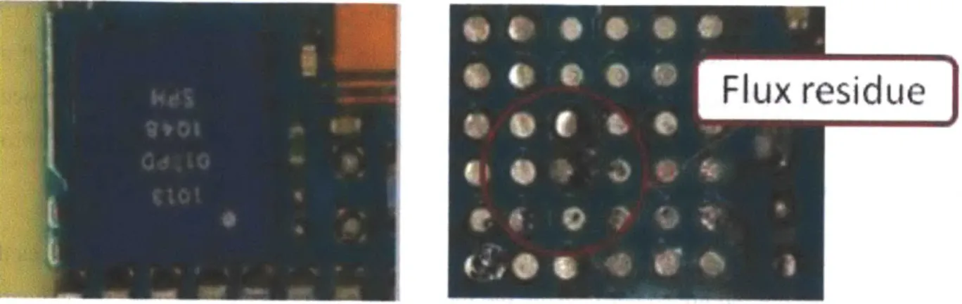
The PCB board cleaning station or the water wash station comes after the second reflow process and the manual inspection stage. The DI water based centrifugal washing machine is responsible of removing all flux residue and other contaminants from the surface of the boards and the modules contained in them. However as illustrated in Figures 3-2 and 3-3, over a period of time it was found that repeated quality tests showed the presence of flux residue on the products. With the objective of maximizing product efficiency and reducing product failure rates, this occurrence was termed as highly avoidable and had to be investigated and corrected.
Flux residue
Figure 3-2 Presence of flux residue under a BGA-FET
Flux residuel
Figure 3-3 Presence of flux residue under chip capacitor array
As per process design, the testing of all components is carried out after the last stage of packaging that is the J-lead mounting cycle. The test cycle inspects all components for their electrical integrity. When components are found faulty, they are sent to the quality department for quality analysis (QA). The QA cycle involves a wide range of tests of which destructive testing is the main procedure, where the surface mounted components are pried out off the PCB board and then inspected for integrity of solder joints, solder shorting, presence of flux residue etc.
Over a period of time since the introduction of the particular product nearly all packages were found positive for flux residue presence. Flux reside was observed on the board and also
under surface mount components. It should be known that as the test cycle is at the end of the assembly line, the cause of fault cannot be cornered onto a particular process and only possible causes can be discerned. It was the management's viewpoint that although it cannot be definitely proved that products were failing due to the presence of flux residue, the issue was stark enough to be worked on.
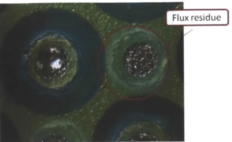
3.1.1 Areas of Residue Incidence on PCB
The inspection or products revealed the presence of flux residue in nearly all inspected products on the board near and around solder joints and under certain components.
a) Near and Around Solder Joints
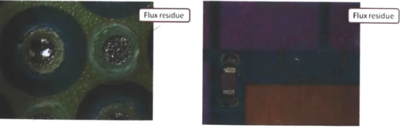
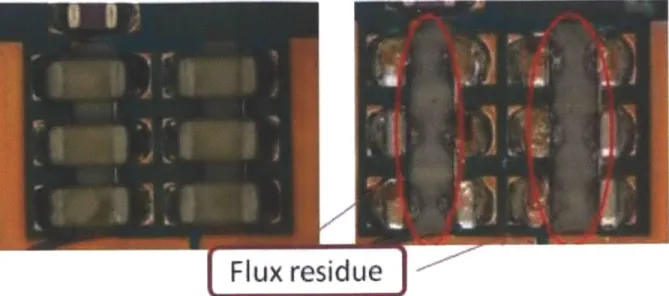
Once the mold compound was cut off the products white colored flux residue was observed on the surface of the PCB board. As shown in Figure 3.4, the residue appeared as a random scattering of white colored particles in clear areas or as rings surrounding solder balls. Further inspection proved them to be water-soluble flux residue that was left behind due to inefficient cleaning.
ix residue
Figure 3-4 Flux residue around BGA's and on board i residue J
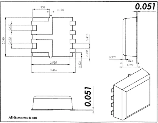
b) Under "low standoff" components
The term "standoff' refers to the distance between the bottom surface of surface mount components and the top surface of the PCB board. As the products being manufactured are
highly compact the components such as 1201 chip capacitors and MLP-FET have standoffs
lower than 50pm. Figure 3-5 illustrates the definition of a "standoff', it shows a MLP-FET whose distance between the bottom surface of the controller and the surface of the PCB board is
50pm. In reality this distance is just about the thickness of the copper laminate that forms the
electrical network i.e. the components are virtually placed flush with the PCB surface with only the copper laminate forming a very small gap. The difficult to remove solder flux residue from these in small gaps is shown in Figure 3-6, an image of the underside a MLP-FET which has
significant flux residue along the leads.
0.051
All dimensions in mm
Fux residue
Figure 3-6 Flux reside on bottom surface of MLP-FET
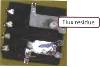
Similarly, quality assurance inspections revealed that nearly all components with low standoffs contained solder flux residue. As illustrated in Figures 3-7 and 3-8, components such as
QMOS, chip capacitors showed presence of flux residue when they were pried off the PCB
board.
Fluxreiu
Figure 3-8 Flux reside on chip capacitor array footprint
3.1.2 Effects of Flux Residue
The presence of flux residue on the surface of the PCB board and under component adversely affects the product inefficiency as highlighted in Section 2.2.2.
3.1.2.1 Electromigration
Electromigration is an electrochemical process where metal on an insulating material, in a humid environment and under an applied electric field, leaves its initial location in ionic form and re-deposits somewhere else[15]. Such migration may reduce isolation gaps and ultimately lead to an electrical short circuit. Electromigration may affect the reliability of flip-chip solder joints as the eutectic solder used is a two-phase alloy, so its electromigration behavior is different from that in aluminum or copper interconnects.
The presence of flux residue on the modules could provide a path for development of a potential [8]. The process starts if a thin continuous film of water along with residue forms an
oppositely charged electrode. Positive metal ions are formed at the positively biased electrode anode, and migrate toward the negatively charged cathode. Over time, these ions accumulate as metallic dendrites, reducing the spacing between the electrodes, and eventually creating a metal bridge. The formed metal bridge would cause solder shorting when potential is applied thus inhibiting the proper functioning of the module.
3.1.2.2 Poor Mold Compound Adhesion
In the manufacturing process once all the components are mounted on to the PCB board the products move to the molding cycle. In this process the products with underfill under the components are molded to encapsulate the package. This process involves covering a molten material over the components which is then allowed to cool to forma hard cover to protect all the surface mount components. This process involves adhesion of the mold compound to the PCB board, for this to take place efficiently the PCB should be clean and free of any contaminants.
Furthermore the manufacturer is moving to replace the current molding process by a "molded underfill" process. This removes the underfill stage completely as the mold compound is used for both molding the product and also as the underfill material. As the mold compound has lesser surface tension than the conventional underfill material, the presence of flux residue and contaminants would make under filling much more difficult.
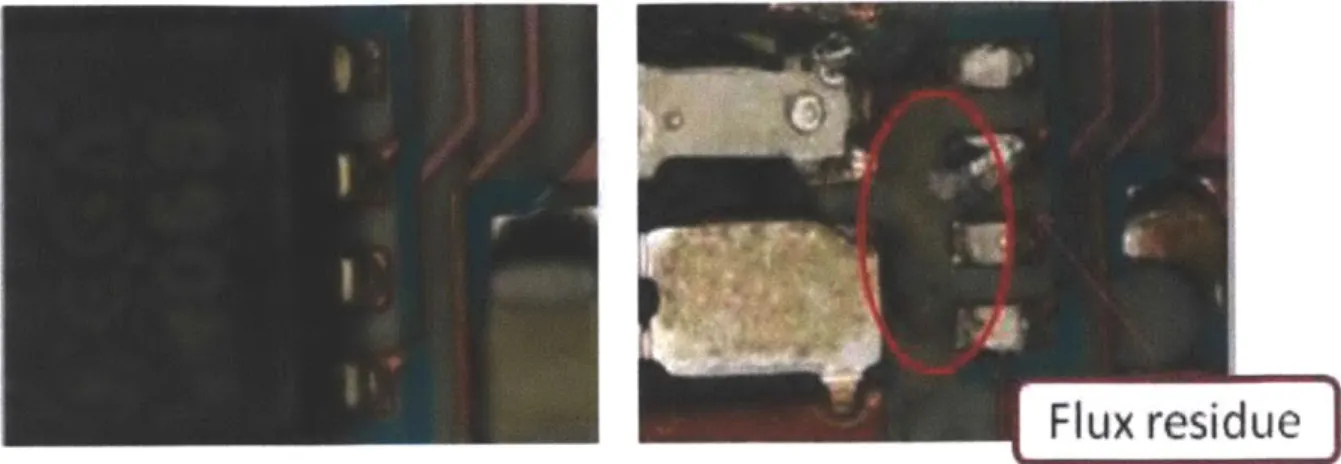
3.1.2.3 Improper J-Lead Attach
Similar to the issue of poor mold compound adhesion the attachment of J-Leads is severely affected by the presence of flux residue near and around the BGAs. The occurrence of flux such as the case illustrated in Figure 3-9 hinders proper soldering of the Lead to the BGA. The J-lead is attached to the BGA in the same way as all other components, it is first placed onto the
BGA and then the unit is passed through a reflow process were the temperature profile fuses the
Flux residue
Figure 3-9 Flux reside around BGA older balls
Hence, if flux residue is present on the surface of the solder balls and also around its periphery the solder joints formed would be contaminated producing solder joints which lack the structural integrity desired.
3.2 Factors Involved
The centrifugal washing process removes solder flux residue from the PCB boards by either physically washing out flux residue or by chemically dissolving it. The principal factors that determine process efficiency are the process variables which contribute to the physical and chemical energy generated in the cleaning process which are agitation, chemical action, wash time and temperature of cleaning solution.
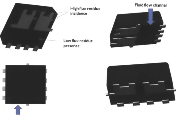
3.2.1 Agitation
The type and magnitude of agitation determines whether sufficient agitation is generated for the solvent to flow into low standoff region. This would firstly help to loosen the flux residue to
flush it out and secondly expose the flux residue to the solution which would simply dissolve it. In the current process, agitation is provided by the centrifugal action of the wash tank and also by two sets of nozzles. As the centrifuge rotates the DI water contained in it attains a state of turbulence, this enables DI water to flow into low standoff regions. The nozzles provide additional agitation by spraying DI water into low standoff regions to wash and rinse the PCB boards.
High flux residue Incidence
Low flux residue presence
Fluid flow channel
I
-Fluid flow channel
Figure 3-11 Presence of flux residue due to improper agitation and fluid flow
3.2.2 Chemical Action
The chemical characteristics of the solution determine how effectively the flux residue is dissolved. Solutions with saponifying agents act to reduce adhesion of solder flux residue to the PCB board; they reduce surface tension of cleaning medium for effective penetration into low standoff areas and then chemically acts on the residue and helps dissolve it. The current process does not use any form of saponifier and uses only DI water during the wash process because of the belief that with enough agitation, water would be able to access low standoff regions to dissolve flux residue. It is to be noted that as the flux residue is completely water soluble in nature, water is sufficient to dissolve it completely, and any other chemical agent assists only in reducing the surface tension to enable DI water to flow into low standoff regions.
3.2.3 Wash Time
Along with agitation and chemical property another important factor is the duration of the wash process. Higher wash times would provide more exposure time of the boards to DI water for loosening and dissolving of flux residue. As the agitation generated by a centrifuge is random,
longer wash times would allow for a much higher chance for the DI water to access low standoff regions.
3.2.4 Temperature
The fourth most important factor is the temperature of the washing solution. As water solubility increases with increase in temperature higher wash cycle temperatures would improve cleaning efficiency; as explained in Chapter 4 this phenomenon has been proven in past studies and experiments. Furthermore, in saponifier based cleaning increased temperature increases the chemical activity of the saponifier. Other benefits of higher temperature are improved solubility of residue and lower surface tension of water.
3.3 Project Objectives
In the Section 3.1 and 3.2, it was seen that effective removal of solder flux residue is vital for product manufacturability and reliability. Thus, it becomes imperative to develop a cleaning process which removes solder flux residue from products, while achieving maximum production speed and quality with minimum cost. To achieve these objectives the research team set out to tackle the problem by splitting it into the following parts:
e Identify the root cause of the flux residue problem through hypotheses formulation and experimental validation.
" Determine optimal process parameters to select and optimize most suitable cleaning
process
e Perform manufacturing system analysis to monitor and study the effect of developed process on system efficiency.
This particular thesis deals chiefly with the second part with brief elaboration of the first and third parts. The work of Jain [1] explains in detail the root cause analysis of the problem, while Rajendran [2] illustrates on the findings of the developed manufacturing systems simulation model. In subsequent chapters, the selection and development of an optimized cleaning process has been discussed.
4. Literature Review
The importance of efficiently removing solder flux residue from components is well appreciated within the electronics manufacturing field [6]. With the increasing miniaturization of electronic assemblies, electronic products are moving to smaller size, higher density, higher speed and lower cost [5, 9]. Furthermore, in the mid 1990's environmental regulations resulted in the implementation of international standards such as RoHS and REACH [6] which pushed the electronics manufacturing industry towards halogen free and lead free soldering. As a result of such technological advancements and environmental regulations, designers and manufacturers are faced with the challenge to maintain acceptable standards of cleanliness.
The ability to remove flux residue after a soldering process from a electronic component is dependent of various factors of which product architecture and the solder flux used are the two most important[10]. The family of products studied in this work is comprised of surface mount technology components which are either chips scale packages (CSP's) or ball grid array
BGA components. BGA components such as FET's have significantly higher standoff heights as
compared to CSP's [12]; their standoff heights range from 457pm to 508 pm while CSP's could have standoff heights less than 50 pm. Research by Mearig and Goesrs [12] has shown that cleaning under BGA's is not a difficult process using semi-aqueous cleaning solutions; on the other hand the significantly smaller standoff heights of CSP's have found to be very difficult to be cleaned by numerous academic and industry studies [4, 5, 7, 8 and 10]. The standoff heights of CSP's were found to vary from component to component due to variation in manufacturing of their lead frames and the minimum standoff height was found to be 30.5 ym [7] .To tackle the
problem of cleaning components with low standoff heights the industry has strived to achieve the optimal combination of type of solder flux and the cleaning technique used to clean it.
After the implementation of environmental regulation the two major families of solder flux used are conventional lead free solder fluxes and no-clean solder fluxes. A majority of the industry leaders have adopted no-clean fluxes [5] due the non-requirement of a cleaning process which facilitates it to be used in complex product architectures [4]. However, it has been seen that in some cases even no-clean solders are cleaned to remove contaminants [7] and it produces process variations during component placement. The products researched in this study were manufactured using a water soluble lead free solder paste as prior experiments using no-clean solder fluxes had resulted in high assembly failure rates. The change in the composition in lead free solder pastes has had significant effects on the physical characteristics of the solder paste such as the melting point and the required reflow temperatures [4]. Due to higher reflow temperatures there is a high probability of a tin-salt formation along with increased bonding between the fluxes and the panel base. Hence, although lead free solder systems are environmentally desirable the cleaning of the flux residues is more difficult [10].
With the adoption of complex solder systems the utilization of appropriate cleaning process is critical. In seminal studies such as [7] & [15] in-line DI water cleaners were used however such cleaning systems are associated with significant capital costs and running costs. Lee in his studies [4, 6 and 10] has stated that mechanical agitation is an important factor in the cleaning process techniques such as spray-in-air, spray-under immersion, ultrasonic waves and centrifuge have been found to show consistently good results. The chemical concentration of the solvent used during the cleaning process has also been found to be a critical factor [10]. Semi-aqueous and Semi-aqueous solvents when used along with appropriate agitation techniques give good cleaning efficiencies. Lee also states that test procedures such as SIR, ionic contamination and ion chromatography have characteristics which make it suitable for a particular flux type and with each test having its advantages and disadvantages.
Prior to this work a study was carried out by the product manufacturers to optimize the DI water based centrifugal cleaning process that was used in the SMT assembly line [3]. The study found that cleaning water temperature, extended wash time, position of product in washing fixture and wait time after reflow did not change the amount of flux residue found on the product after cleaning. Consequently, the proven inefficient of the DI water based centrifugal cleaning process emphasizes the need for adopting a technique that is best suited to the architecture of the product being manufactured and the water soluble lead free solder flux being used. This literature illustrates the study that was carried out applying findings from literatures mention above to develop and optimize an efficient cleaning process.
5.
Cleaning Process Development
The process of developing an optimal technique to remove solder flux residue required understanding of the root cause of the problem. To achieve this objective, the physics of the centrifugal washing process was studied. This involved studying the flux chemistry, agitation effects, chemical methods of cleaning and the dynamics of flow of the cleaning medium [1]. Based on study it was hypothesized that the repeated occurrence of solder flux residue after the centrifugal DI water wash process was due to the low standoff heights of the surface mounted components. The inability to remove flux residue from low standoff regions was due to three possible factors:
e Adhesion of solder flux residue on PCB Board and components, preventing physical flushing out of residue.
" Ineffective agitation generated by cleaning process to access low standoff regions,
preventing chemical dissolution and physical flushing out of flux residue.
* Hindrance to the flow of cleaning solution due to component and product architecture issues.
In his work [1], Jain explains the basis of these hypotheses and how they would help decipher the root causes of the solder flux residue problem. In order to understand the root causes these hypotheses were tested for validity through a series of experiments.
5.1 Root Cause Hypothesis Validation
To understand the root cause of the problem a series of detailed experiment were carried out to test the validity of the developed hypotheses. The tests were designed to help identify the critical factors responsible for inefficient cleaning. To simulate the actual production process the experiments were designed to be carried out within the production cycle. The validation experiments were carried out by introducing a new process station between the final inspection and water wash cycle. As illustrated in Figure 5-1, this station named "Pre-Wash Test Cycle" allowed the ability to vary the factors explained in Section 5.1
Top Solder Final Inspection Pre-Wash Test Water Wash
Reflow
Ese
Cycle 0 CycleFigure 5-1 Hypotheses validation experiment process flow
5.1.1 Pre-Wash Test Cycle
To test the validity of the developed hypotheses and to find out the critical factors determining process efficiency, all process parameter were required to be varied. The water wash cycle was converted to a prewash and water wash cycle to study the change in cleaning efficiency with change in agitation, temperature, time and solution concentration. The pre-wash cycle effectively became the stage where the solder flux residue was acted upon either physically or chemically and the water-wash acted as more of a rinsing cycle to flush away the dissolved flux residue.
5.1.2 Design of Experiments
To test the validity of the formulated hypotheses the four primary process parameters were varied in the soak/ultrasonic process. The different process parameters are detailed in Table 5-1.
Table 5-1 DOE process parameters
Process Parameters Factor Levels
Type of Agitation Ultrasonic, Soak
Deionized Water Concentration of Cleaning Solution 5,7.5, 10 & 12.5 Chemical B (conc. % by volume)
7.5 Chemical A
Process Time (minutes) 2, 5 ,10, 20, 40, & 60
Cleaning Solution Temperature (*C) 60 , 70
The experiments were performed in the following two stages: Stage 1: Hypotheses Test Experiment
In this stage all factor levels were varied to find out the effect of each process parameter on cleaning efficiency. To do this, a flexible DOE was developed (Appendix A) to understand the variation of each process parameter.
Stage 2: Water Wash Process Optimization and Test for repeatability
The centrifugal water wash cycle was retrofitted to allow introduction of Chemical B into the wash cycle. This formed the second stage of the experiment where cleaning efficiency of the water wash process was studied with variation in the concentration of the cleaning solution. Furthermore, this stage also involved repetition of important Stage 1 experiments to test for repeatability of test results as in Appendix A.
5.2 Experiment Methodology
The experiments were carried out by placing each individual PCB board in its designated cleaning recipe in a water bath and subjected to either ultrasonic agitation or plain soak without any external agitation. After the stipulated time, the boards were immediately processed through the 20 minute centrifugal water wash cycle followed by drying in a dry chamber. Once the boards were completely dry, they were subjected to inspection to determine the presence of flux residue in the sample.
5.2.1 Equipment and Test Board
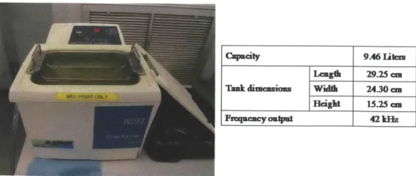
The equipment used as the pre-wash test cycle was the "Cole-parmer 8893 ultrasonic cleaner" shown in Figure 5-2a. This particular cleaner had been used in the assembly line to clean misprinted PCB boards and was retrofitted to conduct the designed experiments. The equipment was chosen as it had a water bath with a 9.46 liters capacity which enabled the tested board to be immersed completely in the cleaning solution. Furthermore the equipment was capable of heating chemical solution up to 750 C, providing ultrasonic vibration with 42 kHz frequency and accurately monitoring experiments times.
Capacity 9.46 ]Lib=
Leng&h 29.25 cm Tank dim iou Wid&k 24.30 an Height 15.25 cm
Frequmay pat 42kHz
The power module "VI Chip- Full TV-36372" shown in Figure 5-2b was selected as the test vehicle. Figure 5-3 shows the PCB boards that contain 16 of these power modules with surface mount components. This particular product was selected as the test vehicle as it provided an architecture that was highly dense with several components having critically low standoff of less than 50pm. As it can be seen in Figure 5-3 the product architecture has dense surface mount components such as 1210 Chip Capacitors and MLP FET's on either side of the product.
PCB Board Top Side
PCB Board Bottom Side
Figure 5-3 Experiment test board: V.1 Chip-TV-36372
5.2.2 Inspection Methodology
The objective of inspection of the sample boards was to generate information of flux residue incidence. The sample boards, once water washed and dried were inspected in the Quality Assurance Laboratory in the production facility. Figure 5-4 below illustrates the flow chart of the inspection process implemented.
From, WashWater
Board Level Visual Inspection
Removal of Top and Bottom Side Components
Top and Bottom Component Underside inspection and grading
Top and Bottom Component
Footprint inspection and grading
To testing /storage
Figure 5-4 Inspection process flow chart
Stage 1: Board Level Visual Inspection and Component Removal
The first stage of inspection involved visual inspected for board level anomalies such as discoloration of copper pad, missing component, deformation and visible solder flux residue. Board inspection was followed by precise removal of components from the top and bottom side
using precision hammer and chisel. Module Numbers 4, 8, 9, and 13 in Figure 5-3 were inspected from each board. These boards were selected to provide an estimate of cleaning efficiency across the architecture of the PCB board. Modules numbered 4 and 9 were inspected as they were positioned in the middle of the center board and modules numbered 8 and 13 were selected as they were positioned on either end of the PCB board.
TOP SIDE Label # Component 1,2,3 BGA FET 4 0603 Chip Capacitor 5,9 CSP-IC PRM2 6 MLP Controler 7,8 0402 Resistor BOTTOM SIDE Label # Component Transducer 2 MLP FET 3 0603 Chip Capacitor 4:11 1210 Chip Capacitor
Figure 5-5 Inspected components on top and bottom side of power module
As illustrated in Figure 5-5 a total of 20 components were pried off each module making it a total of 80 components for inspection per board. On the top side 9 components such as
BGA-FET, 0603 Chip Capacitors and MLP were studied as all of them possessed standoff in the rage
of 50 ym tol0im. The BGA-FET was critical as the component was mounted on an array of